Modelling of MIB Based SPLDs for Future
Computing
Dr. J Gope#1, Rahul Kumar Sah#2, Sanjay Bhadra#3, Mahuya Panda#4
#1
Department of ECE, Camellia School of Engg & Tech., West Bengal University of Technology
#234
Department of EEE, Camellia School of Engg & Tech., West Bengal University of Technology
Abstract— Designing low power ultra dense digital circuits are considered both fascinating and challenging technology in
post CMOS era. SET (Single Electron Transistor) technology came up as a promising candidate and is largely accredited owing to their higher acceptability in today’s academia and industry. This research endeavour insights the novelty of SETs in the vicinity of fabrication and room temperature operation. But in both the cases SETs is some how lagging behind. In such, a comparatively new concept of hybridising CMOS with SETs reveals new prospect in device research. The Mahapatra-Ionescu-Banerjee (MIB) model based on this hybrid CMOS-SET is pioneer in bridging the gap in CMOS and SETs. The Authors here demonstrate a hypothetical model of hybrid CMOS-SET Simple Programmable Logic Devices (SPLDs).
Keywords— Single Electron Transistor (SET), Hybrid CMOS-SET, MIB Model, SPLDs, Device Miniaturization, Coulomb
Blockade
I. INTRODUCTION
The processing power of logical and arithmetic circuit implementations augmented manifold during the last few decades. This led to tremendous advancement in algorithms and device technology. The 70’s of 19th century was dominated by Moore’s law doubling the number of transistors in every 18 month in the same chip die-area [1]. There by physical reduction of size in microelectronic circuit along with increase in the number of transistors in same die-area are considered as “Contributing factors to this dramatic increase”. But the Moore’s Law cannot continue forever owing to the inherent limitations of CMOS Technology.
The 2003 edition of International Technology Roadmap for Semiconductors (ITRS) ushered new possibilities leading to Ultra Thin Body (UTB) MOSFETs having gate-lengths up to 10nm [2]. Besides, the electrical currents will shrink down to individual electrons which are known as Quasi-Ballistic Mode. This leads to abrupt change in future device switching behaviour and thus it was largely anticipated that fundamental physical dimension of CMOS devices will lead to its extinction rapidly. Consecutively several future candidate technologies based on new operating principle evolved and presently attributed as the research topic of device scientist worldwide. Few recommended reporting’s of such technologies are Carbon-Nano (CN) tubes , Resonant tunnelling diodes (RTD), Magnetic Spin Devices, Single Electron Transistor (SET) [3].
The Authors here have limited themselves in studying practical orientation of SET Devices. However subsequent few paragraph in this manuscript will lead to hybridisation of CMOS and SET as because total replacement of CMOS with SET is some how is not accessible with the presently known existing technologies [4]. This is why authors tendered to work with MIB model of Hybrid CMOS SET in designing next gen simple PLD. Section II briefly describes SET followed by concise analytical study of hybrid CMOS SET. Section IV briefly enumerates the hypothetical approach of Hybrid CMOS SET based SPLD and its modus operandi. The last section is of theoretical investigation described in the form of comparative statement to potentially advocate the incorporation of Hybrid CMOS SET based future modelling of devices.
II.SETINBRIEF
[5-Technology (IJRASET)
10]. But background charge problem and low gain remain crucial research topic in mobilising in theoretical fundamentals into physical implication of SET based device [11-13]. This is why few Researchers have feared that complete replacement of CMOS using SET is not feasible with the existing Lithography techniques. Following are SET based logic gates.
Figure 1.Schematic Structure of SET
Figure 2.TWO Input SET based AND Gate [image:3.612.57.516.107.328.2]
Figure 3.TWO Input SET based OR Gate Figure 4.TWO Input SET based NOT Gate
III.HYBRIDCMOS
Prof S.K. Sarkar and his team reported hybridisation of Schmidt trigger based on CMOS and SET [14]. During this tenure hybrid CMOS-SET emerged as an unbeatable candidate for next gen computing. Characteristically SETs and FETs are never identical; rather they are complimentary. SET is the offspring of Ultra Low Power Highly-Integrated device structures having numeral functionalities in threshold logic, whereas CMOS posses’ high speed driving and high voltage gains like properties. Thus for SET to compete head to head with CMOS technology requires Hybridisation with existing CMOS Technology. As the name reveals it is a composite structure having its pull-up network based on CMOS and the pull-down is comprised of SET. Prof Santanu Mahapatra introduced the MIB model of hybrid CMOS-SET which is quite advantageous than normal SET considering the advantageous low current drive, lacking of room temperature operation for massive production and background charge problems [15-17]. Such Incorporation paves new dimension in device research by introducing new functionalities of transport properties of electrons which leads improved massive of device manufacturing. From the very inception the notion of Hybrid CMOS SET reveal overcoming of intrinsic limitations of CMOS and manufacturing drawbacks of SET. Thereby both in industry and academia hybrid CMOS SET are a promising alternative. Very recently TOSHIBA demonstrated empirically performance of Hybrid CMOS SET Inverter in their patented Hybrid Low power VLSI Design [18].
SET, when exploited to function as a switching element it has to overcome the Coulomb Blockade barrier i.e. the off-state, thereby permitting to conduct current i.e. on state. There after it mimics the MOSFET Logic architecture. In case of Hybrid CMOS SET PMOS transistor acts as a load resistance of a SET. Thus it is required to imply some design rules. Following are few Logic Gates based on Hybrid CMOS SET structures.
[image:3.612.115.179.588.680.2] [image:3.612.350.455.595.674.2]
Figure 7.TWO Input Hybrid CMOS based OR gate
IV.SPECIALPROGRAMMABLELOGICDEVICES(SPLDS)
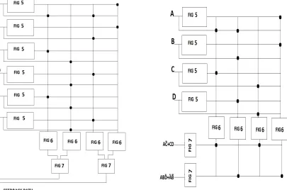
[image:4.612.91.292.297.572.2] [image:4.612.101.506.302.570.2]In fig 8 & fig 9 the authors incorporated hybrid CMOS SET based logic devices to implement simple PAL & PLA to study the robustness of Nano- IC (NANO SPLDs). The modus operandi of such Nano IC’s follows the simple switching conversion of SET. The Co-Integration model allows place sharing of SET’s with their conventional counterparts of MOSFET devices in the same die-area; here the Vdd is defined by SET device parameter. Employing a uniform interval clock pulse the model will deliver interrupted processing of information with error free high potentiality. For the time being the authors have limited themselves in soft computing studies of the proposed model using T-Spice.
Figure 8.Programmable Array Logic(PAL) Figure 9.Programmable Logic Array (PLA)
V. RESULTS
ABCD are the four inputs of Fig.8. With the first clock pulse ‘ ’ the voltage across the dotted terminals becomes high than the Coulomb Blockade, the transport phenomenon of electrons occurs in Fig.6. The output of Fig.6 is fed to the input of Fig.7
during the corresponding clock pulses i.e. . The process is mimicked subsequently in the next part of the circuit. Thereafter we received the outputs which are fed to the input of Fig.5. Thus the feedback path is generated which controls the driving mechanism of the proposed programmable array logic(Fig.8).
Technology (IJRASET)
The authors typically rendered upon Tanner tools and BSIM modelling to hypothetically design this nano ICs to be incorporated in future high speed, low power consuming devices. The authors further more emphasised to attain the maximum ‘trade off’ between the generated CMOS based architecture and the proposed design. The same is being tabled below.
TABLEI
CIRCUIT TYPE POWER SUPPLY NUMBER OF
CMOS
NUMBER OF
SET
POWER
CONSUMPTION
FIG.6 0.01V 3 3 1.02E-09W
FIG.7 0.01V 3 3 1.02E-09W
VI.CONCLUSION
To increase the efficiency of monolithic CMOS IC’s hybrid CMOS SET based SPLD’s has been analytically studied here in this manuscript. A comprehensive investigation revealed that a power consumption of 1.02e-09 watt is used by the AND gates in the AND array and also in the OR gates of the OR array. Consequently the power consumption of the circuit drastically dwindles down when compared to conventional CMOS based SPLD’s. Thus such proposed modelling is feasible enough in future low power ultra dense VLSI/ULSI circuits. Also the co integration of CMOS and SET’s can be obtained at room temperature without shadowing their potentialities. The switching speed mobility and power dissipation shows enhanced acceptability. Thus such modelling is anticipated to mobilise the next gen SPLDs.
VII. ACKNOWLEDGMENT
We hereby acknowledge the kind technological and financial support provided by Prof. (Dr.) A. S. Chowdhury, Hon’ble Director of Camellia School of Engineering and Technology, West Bengal, INDIA to carry out this rigorous research.
REFERENCES
[1]. Moore,Gorden.E(1965).”Cramming more components onto integrated circuits” Electronics magazine. P.4.retrieved.2006-11-11. [2]. Pollack F. Intel 1999.In:The International Technology Roadmap for Semiconductors,2005.
[3]. T.A.Fulton aand T.J.Dolan, Phys.Rev.Lett.59,109(1987)
[4]. Daniel Rairigh “Limits of CMOS Technology Scaling and Technologies Beyond-CMOS”2001
[5]. Likharev, K.K., On the Possibility of Fabricating Analog and Digital Integrated Circuits Based on Discrete Single-Electron Tunneling, Mikroelektronika, 1987, vol. 16, no. 3, pp. 195–209
[6]. S. Mahapatra, A.M. lonescu, K. Banejee, M.J.Declerq, “Modelling and analysis of pow- dissipation in single electron logic”, Technicol Digest oflEDM 2002.
[7]. K. Uchida, 1. Koga, R. Ohba, A. Toriumi, “Programmable singleelectron transistor logic for iow-power intelligent Si LSI”, ISSCC 2002, Vol. 2, pp. 162453.
[8]. S. Mahapatra, A.M. lonescu, K. Baneiee, “A quasi-analytical SET model for few electron circuit simulation”, IEEE Electron De”. Lett., Vol. 23,No. 6,pp. 366-368,2002
[9]. S. Mahapatra, V. Pott, S. Ecoffey, A. Schmid, C. Wasshuber, J. W. Tringe, Y. Leblebici, M. J. Declercq, K. Banerjee, and A. M. Ionescu, “SETMOS: A novel true hybrid SET-CMOS high current
[10].Coulomb blockade oscillation cell for future nano-scale analog ICs”, in Proc. of IEDM, 2003, pp. 703-706.
[11].J. S. Park, T. Saraya, K. Miyaji, K. Shimizu, A. Higo, K. Takahashi, Y. Yi, H. Toshiyoshi, and T. Hiramoto, “Characteristic modulation of silicon MOSFETs and single-electron transistors with a movable gate electrode”, in Proc. of IEEE SNW, 2008, S1015.
[12].L. Qin, C. Li, Z. Youjie, W. Gang, and W. Sen, Design and simulation of logic circuits by combined single electron and MOS transistor structures, Proc. IEEE Intl. Conf. Nan/Micro Engineered and Molecular Sys., January (2008).
[13].C. Sathe, S. S. Dan, and S. Mahapatra, “Assessment of set logic robustness through noise margin modeling,” IEEE Transactions on Electron Devices, vol. 55, no. 3, pp. 909–915, 2008
[14]. Nakazato, K. and Ahmed, H., Enhancement of Coulomb Blockade in Semiconductor Tunnel Junction, Appl. Phys. Lett., 1995, vol. 66, pp. 3170–3172. [15].Anindya Jana, N Basanta Singh, Anup Sarkar, J.K.Sing and Subir Kumar Sarkar, “Design and Implementation of a Hybrid SETCMOS based Hi-speed and
power efficient Pulse Divider Circuit” Chennai and Dr.MGR University Second International Conference on Sustainable Energy and Intelligent System (SEISCON 2011), Dr. M.G.R. University, Maduravoyal, Chennai, Tamil Nadu, India. July. 20-22, 2011.
[16].Jayanta Gope et.al., “Analytical Modelling of hybrid CMOS-SET based Moore and Mealy Logical Circuit”, IPASJ International Journal of Computer Science(IIJCS),May 2014.
[17]. Jayanta Gope et.al., “Implementation of Decision Making Sub System using SET and Hybrid CMOS-SET –A Case Study” ,International Journal of Advanced Research in Computer Science and Software Engineering, June 2014.
[18].Jayanta Gope et.al., “Modelling of Hybrid CMOS SET based highly efficient Parallel-In-Serial-Out Shift Register for next generation electronics.June 2014(IJEMR)