An Efficient Design of 2:1 Multiplexer and its
Application in 1-Bit Full Adder Cell
Ila Gupta
Neha Arora
B.P. Singh
Deptt. Of ECE Deptt. Of ECE Professor, Deptt. Of ECE
FET-MITS (Deemed University)
FET-MITS (Deemed University)
FET-MITS (Deemed University)
Lakshmangarh Lakshmangarh Lakshmangarh
ABSTRACT
A multiplexer, sometimes referred to as a "mux", is a device that selects between a numbers of input signals. It is a combinational logic circuit. It is a unidirectional device and used in any application in which data must be switched from multiple sources to a destination. This paper represents the simulation of different 2:1 Multiplexer Structures and their comparative analysis on different parameters such as power supply voltage, operating frequency, temperature and area efficiency etc and its application in 1 bit full adder cell. All the simulations have been carried out on BSIM 3V3 90nm technology at Tanner EDA tool.
General Terms
2:1 multiplexer, Power-delay product and Speed.
Keywords
CMOS Logic, Low power, Full adder, and VLSI.
1. INTRODUCTION
Advances in CMOS technology have led to a renewed interest in the design of basic functional units for digital systems. The use of integrated circuits in high performance computing, telecommunications, and consumer electronics has been growing at a very fast pace. This trend is expected to continue, with very important implications for power-efficient VLSI and systems designs. Low power has emerged as a principal theme in today’s electronics industry. The need for low power has caused a major paradigm shift where power dissipation has become as important a consideration as performance and area [1]. A 2-to-1 multiplexer is a basic building block of the “switch logic”. The concept of the switch logic is that logic circuits are implemented as combination of switches, rather than logic gate. Multiplexers are used in building digital semiconductors such as CPUs and graphics controller, as programmable logic devices, in telecommunications, in computer networks and digital video. This paper compares the different 2:1 multiplexer structures on the basis of the power dissipation, speed, operating frequency range and their temperature dependence with the area efficiency of the circuit and its application in 1 bit full adder cell.
2.
LITERATURE
REVIEW
OF
DIFFERENT
2:1
MULTIPLEXER
STRUCTURES
2.1 NMOS 2:1 Multiplexer Structure
The schematic diagram of NMOS 2:1multiplexer is shown in Fig.1. Pass transistor logic (PTL) describes several designs of circuits. Among them are CPL (Complementary
[image:1.595.352.503.294.405.2]Pass-Transistor Logic) and DPL (Double Pass-Pass-Transistor Logic). It is based on CPL. It reduces the count of transistors. It can only be connected to the source/drain input of another MOS transistor. This reduces the number of active devices, but has the disadvantage that output levels can be no higher than the input level [2].
Figure 1. Schematic of NMOS 2:1 Multiplexer
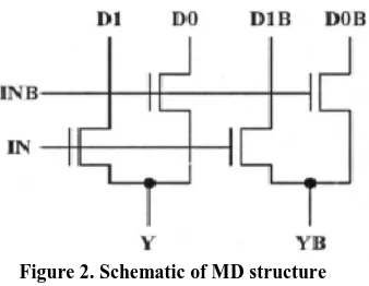
2.2 MD 2:1 Multiplexer Structure
[image:1.595.349.518.492.623.2]The schematic diagram of MD 2:1 multiplexer is shown in Fig.2. MD stands for multiplexer double. With the help of this circuit we find the inverted output also [3].
Figure 2. Schematic of MD structure
latching circuit and a cascoded complementary logic array. [4]- [8]
Figure 3. Schematic of DCVSL structure
[image:2.595.64.264.356.615.2]2.4 MDCVSL 2:1 Multiplexer Structure
Figure 4. Schematic of MDCVSL structure
MDCVSL stands for modified differential cascode voltage switch logic. If we modify DCVSL circuit by adding two weak p channel devices i.e. transistors T9 and T10 the output of modified DCVSL 2:1 multiplexer will show better results in terms of power consumption, delay, temperature and output load capacitance and operating frequency. The schematic diagram of MDCVSL 2:1multiplexer is shown in Fig.4 [4] - [8].
3. SIMULATIONS AND COMPARISON
3.1 Simulation Environment
A simulation of various 2:1 multiplexer are done using Tanner EDA Tool version 13.0. Various 2:1 multiplexer circuits simulations are performed on BSIM3v3 90nm technology with supply voltage ranging from 0.6V to 1.4V. In order to prove that which design is consuming low power and have high performance, simulations are carried out for power, delay, power-delay product at varying supply voltages, temperatures and operating frequencies. To establish an impartial simulation circumstance, each circuit have been tested on the same input patterns which covers every possible combination of input a, b and s.
3.2 Simulation Analysis
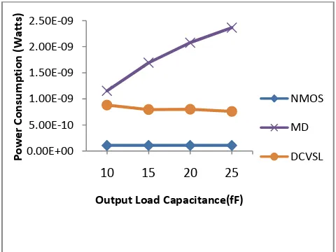
[image:2.595.316.552.377.525.2]The graph shown in Fig.5 reveals that the power consumption of DCVSL circuit is remarkably reduced than the other approaches at 90nm technology. The delays of all the circuits are shown in Fig.6. MDCVSL approach shows slightly less delay than the delay of other design for input voltage ranging from 0.6V to 1.4V. Similar results for power consumption vs. temperature and power consumption vs. output load capacitance are shown in Fig.7, Fig.8, and Fig.9 respectively at 90nm technology. As it is found from the simulations MDCVSL circuit shows better performance for the range of temperature and output load capacitance among all the other design approaches for 2:1 Multiplexers.
[image:2.595.315.556.495.716.2]Figure 5. Power consumption comparison of various 2:1 multiplexer technologies at different supply voltages
Figure 6. Delay comparison of various 2:1 multiplexer 0.00E+00
5.00E-10 1.00E-09 1.50E-09 2.00E-09 2.50E-09 3.00E-09 3.50E-09 4.00E-09
.6v .8v 1v 1.4v
Po
we
r
C
o
n
sump
ti
o
n
(Watt)
VDD(Volt)
NMOS
MD
DCVSL
MDCVSL
1.80E-08 1.85E-08 1.90E-08 1.95E-08 2.00E-08 2.05E-08 2.10E-08 2.15E-08 2.20E-08 2.25E-08
.6v .8v 1v 1.4v
D
e
lay
(Sec
o
n
d
s)
VDD(Volt)
NMOS
MD
DCVSL
Figure 7. Power consumption comparison of various 2:1 multiplexer technologies at different temperatures
Figure 8. Power consumption comparison of various 2:1 multiplexer technologies at different output load
capacitance
Figure 9. Power consumption comparison of various 2:1 multiplexer technologies at different output load
capacitance
Table 1 show the power delay product over a range of power supply voltages and as it is shown in the table that MDCVSL circuit for 2:1 multiplexer show minimum Power delay product.
Table 1: Power delay product comparison of different 2:1 multiplexer structure
Different 2-To-1 Multiplex
er Structure
Power Delay Product (90 nm) ( Watt Second)
VDD=.6v VDD=.8v VDD=1v VDD=1.4v
NMOS 2.17E-18 1.71E-17 3.13E-17 7.18E-17
MD 1.39E-17 1.76E-17 5.30E-17 6.56E-17
DCVSL 3.70E-18 1.52E-17 2.00E-17 3.18E-17
MDCVSL 1.94E-18 1.22E-17 1.66E-17 1.61E-17
4. APPLICATION OF MODIFIED DCVSL
2:1 MULTIPLEXER IN LOW POWER
HIGH PERFORMANCE ADDER CELL
4.1 Adder Circuit Using NMOS 2:1
Multiplexer Circuit
Schematic of Adder circuit using NMOS 2:1 multiplexer circuit is shown in Fig.10. This design of full adder circuit is based on three transistor XOR gates and NMOS 2:1 multiplexer. In this circuit the (W/L) ratio for transistor T2 ,T5 are (W/L) n=1/1 and for transistor T1, T4 are (W/L) p=3/1 and for transistor T 3, T6 are (W/L) p=5/1 and for transistor T7, T8 are (W/L)n=7/1 [9],[10].The Boolean equations for the design of this circuit are
𝑆𝑢𝑚 = 𝐴 ⊕ 𝐵 ⊕ 𝐶𝑖 𝐶𝑜𝑢𝑡 = 𝐶𝑖𝑛 𝐴 ⊕ 𝐵 + 𝐴 · 𝐵
Figure 10. Schematic of Adder circuit using NMOS 2:1 multiplexer
0.00E+00 1.00E-09 2.00E-09 3.00E-09 4.00E-09 5.00E-09 6.00E-09
0 10 30 50 70 90
Po
we
r
C
o
n
sump
ti
o
n
(
Watts)
Temperature (°C)
NMOS
MD
DCVSL
MDCVSL
0.00E+00 5.00E-10 1.00E-09 1.50E-09 2.00E-09 2.50E-09
10 15 20 25
Po
we
r
C
o
n
sump
ti
o
n
(
Watts)
Output Load Capacitance(fF)
NMOS
MD
DCVSL
9.20E-11 9.40E-11 9.60E-11 9.80E-11 1.00E-10 1.02E-10 1.04E-10 1.06E-10 1.08E-10 1.10E-10
10 15 20 25
Po
we
r
C
o
n
sump
ti
o
n
(
Watts)
Output Load Capacitance(fF)
MDCVSL
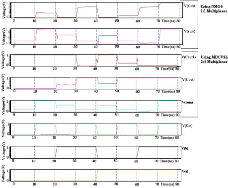
[image:3.595.53.294.333.696.2] [image:3.595.318.559.511.708.2]Figure 11. Schematic of Adder circuit using MDCVSL 2:1 multiplexer
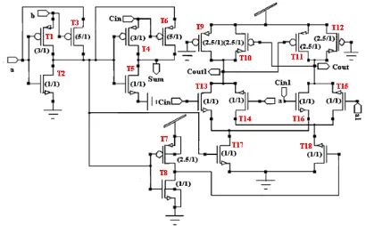
4.2 Adder Circuit Using Modified DCVSL
2:1 Multiplexer Circuit
Schematic of Adder circuit using modified DCVSL 2:1 multiplexer circuit and simulated waveforms are shown in Fig.11. This design of full adder circuit is based on three transistor XOR gates and modified DCVSL 2:1 multiplexer [9],[10]. The Boolean equations for the design of this circuit are as follows:
𝑆𝑢𝑚 = 𝐴 ⊕ 𝐵 ⊕ 𝐶𝑖𝑛 𝐶𝑜𝑢𝑡 = 𝐶𝑖𝑛(𝐴 ⊕ 𝐵) + 𝐴 · (𝐴 ⊙ 𝐵)
5. PERFORMANCE ANALYSIS
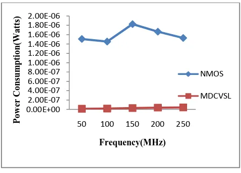
[image:4.595.314.563.364.515.2]The graph shown in Fig. 12 - Fig. 16 reveals that the one bit full adder cell using MDCVSL technology proves superiority in terms of power delay product at varying input voltage and frequency, output load capacitance and temperature sustainability over using NMOS technology. The graph shown in Fig.12 reveals that the power consumption of MDCVSL based one bit full adder cell circuit is remarkably reduced than the NMOS based one bit full adder cell at 90nm technology. The delays of the circuits are shown in Fig.13. MDCVSL based one bit full adder cell circuit shows slightly more delay than the delay of NMOS based one bit full adder cell for input voltage ranging from 0.6V to 1.4V. Results for power consumption vs. temperature and power consumption vs. operating frequency and power consumption vs. output load capacitance are shown in Fig.14, Fig.15 and Fig.16 respectively at 90 nm technologies. As it is found from the simulations MDCVSL based one bit full adder cell is remarkably reduced than the NMOS based one bit full adder circuit shows better performance for the range of operating frequency and operating temperature and output load capacitance. Fig.17 reveal that the power consumption of the MDCVSL based one bit full adder is less than that of NMOS based one bit full adder circuit.
Figure 12. Power Consumption comparison of one bit full adder cell using NMOS and MDCVSL technology at
[image:4.595.315.561.509.725.2]different supply voltages
Figure 13. Delay comparison of one bit full adder cell using NMOS and MDCVSL technology at different supply
0.00E+00 1.00E-05 2.00E-05 3.00E-05 4.00E-05 5.00E-05
0.6 0.8 1 1.4
Po
w
er
Co
n
sum
p
ti
o
n
(Wa
tts
)
VDD(Volts)
NMOS
MDCVSL
0.00E+00 5.00E-09 1.00E-08 1.50E-08 2.00E-08 2.50E-08 3.00E-08 3.50E-08 4.00E-08 4.50E-08
.6v .8v 1v 1.4v
Dela
y
(Seco
nd
s)
VDD(Volts)
NMOS
Figure 14. Power Consumption comparison of one bit full adder cell using NMOS and MDCVSL technology at
different temperatures
Figure 15. Power Consumption comparison of one bit full adder cell using NMOS and MDCVSL technology at
[image:5.595.308.550.91.233.2]different operating frequency
Figure 16. Power Consumption comparison of one bit full adder cell using NMOS and MDCVSL technology at
[image:5.595.54.293.294.466.2]different output load capacitance
Table 2. Power Delay Product Comparison of NMOS and MDCVSL based adder Cell
VDD (volts) Power Delay Product(Watt-sec)
(90nm)
NMOS MDCVSL
.6
4.51105E-14 5.03905E-16
.8
1.99311E-13 1.58825E-15
1
4.58125E-13 4.30337E-15
1.4
1.29024E-12 2.44445E-14
6. CONCLUSION
For low-leakage and high-speed circuits concern should be on both the factors speed and power [11]. This paper concluded with the efficient approach of multiplexer at 90nm technology. Modified Differential Cascade Voltage Switch Logic (MDCVSL) shows least power consumption over a range of power supply voltage, power-delay product, operating frequency, output load capacitance and operating temperature over other circuit design of 2:1 multiplexer. The MDCVSL based 1-bit full adder is found to give better performance than the NMOS based full adder. It shows remarkable improvement in power delay product and has better temperature sustainability. Hence, MDCVSL multiplexer based adder is suitable for lower power high-speed applications. It has a marginal increase in area compared to the NMOS multiplexer based adder; overall, we achieved the lowest power consumption and power-delay product. Fig.17 reveal that the power consumption of the proposed cell is less than that of existing one and thus proposed cell proves its superiority over existing one and hence ensuring the better performance for low power systems.
7. REFERENCES
[1] Kang, Sung-Mo, Leblebici and Yusuf (1999), “CMOS Digital Integrated Circuits Analysis and Design”, McGraw-Hill International Editions, Boston, 2nd Edition.
[2] Yano, K., Sasaki, Y., Rikino, K. and Seki, K. (1996) “Top-down pass transistor logic design”, IEEE Journal of
Solid-State Circuits 31(6), 792–803.
[3] Kiseon Cho and Minkyu Song,” Design Methodology of a 32-bit Arithmetic Logic Unit with an Adaptive Leaf-cell Based Layout Technique” VLSI Design, 2002 Vol. 14 (3), pp. 249–258.
[4] D. Z. Turker,, S. P.Khatri , “A DCVSL Delay Cell for Fast Low Power Frequency Synthesis Applications”, IEEE transactions on circuits and systems june 2011, vol. 58, no. 6, pp. 1125-1138.
[5] F-s Lai and W Hwang, “Design and Implementation of Differential Cascode Voltage Switch with Pass-Gate (DCVSPG) Logic for High-Performance Digital Systems” IEEE journal of solid-state circuits, vol. 32, no. 4, april 1997,pp 563-573.
[6] P. K. Lala and A. Walker, “A Fine Grain Configurable Logic Block for Self-checking FPGAs”,VLSI Design 2001, Vol. 12, No. 4, pp. 527-536.
0.00E+00 2.00E-06 4.00E-06 6.00E-06 8.00E-06 1.00E-05 1.20E-05 1.40E-05 1.60E-05 1.80E-05
0 10 30 50 70 90
Po w er Co n sum p ti o n (Wa tts) Temperature(°C) MDCVSL NMOS 0.00E+002.00E-07 4.00E-07 6.00E-07 8.00E-07 1.00E-06 1.20E-06 1.40E-06 1.60E-06 1.80E-06 2.00E-06
50 100 150 200 250
Po w er Co n sum p ti o n (Wa tts) Frequency(MHz) NMOS MDCVSL 0.00E+00 1.00E-06 2.00E-06 3.00E-06 4.00E-06 5.00E-06 6.00E-06 7.00E-06 8.00E-06
10 15 20 25
Po w er Co n sum p ti o n (Wa tts )
Output Load Capacitance(fF) NMOS
[image:5.595.53.294.392.678.2][7] Jan M. Rabaey, Digital Integrated Circuits; a design prospective, Upper Saddle River: Prentice-Hall, 1996. [8] Heller, L. G. et al., "Cascode Voltage Switch Logic: A
differential CMOS Logic Family", Proceedings of 1984 IEEE International Solid-state Circuits Conference, pp. 16-17.
[9] T. Sharma, Prof. B.P.Singh, K.G.Sharma, N. Arora , “High Speed, Low Power 8T Full Adder Cell with 45% Improvement in Threshold Loss Problem”, Advances in Networking, VLSI and Signal processing pp.272-27.
[10] S. R. Chowdhury, A. Banerjee, A. Roy, H. Saha “A high Speed 8 Transistor Adder Design using Novel 3 Transistor XOR Gates” International Journal of Electronics, Circuits and System s, vol. 2, No. 4, pp.217-223, 2008.
[image:6.595.94.553.200.579.2][11] A. Bellaouar, Mohamed I. Elmasry, “Low-power digital VLSI design: circuits and systems”, 2nd Edition.