Improvement of Compactness of Low Pass Filter Using New
Quasi-Yagi-DGS-Resonator and Multilayer-Technique
Ahmed Boutejdar1, * and Wael Abd Ellatif2
Abstract—A novel 1.8 GHz compact microstrip low-pass filter (LPF) based on quasi-yagi defected ground structure (DGS) and compensated capacitors is proposed in this paper. The filter has a very sharp cut-off frequency response with low insertion loss and achieves a wide reject band with overall 20 dB attenuation from 2.8 GHz up to 10 GHz. The equivalent circuit model of Yagi-DGS-unit is derived using AWR software, and the circuit parameters are extracted by using a simple circuit analysis method. The advantage of this structure is that the reject band can be controlled by tuning the dimension of Yagi-arms at higher frequency rang. The proposed 1.8 low-pass filter is designed using microwave office electromagnetic software and fabricated on the RO4003 ceramic structure with dielectric constant of 3.38. The compact filter occupies an area of (0.45λg ×0.35λg) with λg = 44 mm. A comparison between simulation and measurement results confirms the validity of the LPF configuration and design procedure. In order to improve the compactness of the proposed LPF, a new multi-layer method has been employed. Finally, a new minimized LPF-topology 50% more compact than the conventional is realized.
1. INTRODUCTION
Newly, photonic structures, defected microstrip structures (DMSs) and defected ground structures (DGSs) have gained much interest for their planar topology and easy and inexpensive fabrication with photolithographic technique or printed-circuit board technology [1–5]. Periodic or non-periodic DGSs show a good repressed reject band in some frequency, thus restrain spurious response by repressing harmonic in the microwave circuits [6, 7]. The DGS unit can have a simple geometry (rectangle by Dai et al.) or a complicated shape (fractal as by Boutejdar et al.) to improve the reject band of a low pass filter [8, 9]. Most DGS-structures are used to design and improve filters [10–12], patch antennas [13, 14], branch line couplers [15], dividers [16] and improved efficiency of power amplifiers [17].
A defected ground structure technique is realized by etching a few defect patterns in the backside metallic ground plane under the microstrip line [18–20]. This defect disturbs the shield current distribution in the ground. This disturbance modifies the transmission line characteristics (increase of effective inductance and capacitance) and achieves slow-wave effect and band-stop property. The DGS is often composed of two wide etched areas, which are connected through a thin slot-channel, thus the total structure corresponds to the equivalent parallel LC resonance circuit. In order to find the approach equivalent circuit, two methods can be used:
1. Field distribution method. 2. Simulation-comparison method.
Received 30 July 2016, Accepted 26 October 2016, Scheduled 18 November 2016 * Corresponding author: Ahmed Boutejdar ([email protected]).
1 German Research Foundation DFG, Electrical Engineering, Bonn-Braunschweig, Germany.2Arab Academy for Science, Technology
The parameters of the derived approach DGS-circuit can be extracted from electromagnetic simulation result which can be fit for the one-pole Butterworth-low-pass response.
Based on slow wave effect, the DGS technique is developed and used to suppress the undesirable harmonics, thus to gain a lossless broad stopband and realize compact structures. However, to obtain response with transmission losses in passband and large reject band in stopband using DGS technique, the cascaded DGS method should be used. This leads to a larger size and loss in passband, which is caused by undesired coupling between the resonators.
In this paper, based on our previous work about the rectangular DGS [21–25], rectangular DGS with arms along the slot cannel so-called quasi-Yagi-DGS structure is used to control the coupling between the cascaded resonators in order to improve the reject band, reduce the losses, increase the sharpness of the transition domain, thus minimize the size of the investigated structure. A new very compact low-pass topology is designed and optimized using multilayer technique. The measurements show good agreement with the calculations. The proposed filter has been designed and experimentally characterized to demonstrate usefulness of the proposed Yagi-DGS-idea. Such defected ground structure filters are often required in many RF/microwave applications.
2. THE TOPOLOGY OF THE NEW DGS STRUCTURE AND ITS CHARACTERISTICS
As shown in Fig. 1, the proposed quasi-Yagi DGS-unit consists of two rectangular heads, which are connected through horizontal and vertical thin slot-channels (arms), in ground plane. The square-head with an area of (a×b) presents the inductance, while the slots (g) between them present the capacitance. As shown in Fig. 1, the proposed quasi-Yagi DGS-unit consists of two rectangular heads, which are connected through horizontal and vertical thin slot-channels (arms), in ground plane. The square-head with an area of (a×b) presents the inductance, while the slots with wide (g) and (e) between them present the capacitances. Both vertical thin slot-channels are used to increase or decrease the total capacitance of the Yagi topology and thus to control position of the transmission zero of the S21 -scattering. This technique will be used to improve the compactness of the structure without increasing the size of the proposed topology. The vertical and horizontal thin slot-channels are presented by
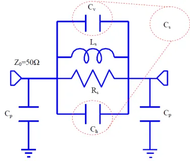
Cy and Ch. Fig. 2 shows an approach lossless equivalent circuit, based on Tchebycheff’s π-network, whereCS is the sum of capacitances in the ground andLS the parallel inductance toCS. The parallel
capacitance CP, between the microstrip feed and the metallic ground, describes the influence resulting
from the fringing field around the DGS unit. The resistance RS presents the losses resulting from the
radiation and dielectric substrate. The circuit model is devised using microwave office simulator. The equivalent circuit parameters can be calculated from the S-parameters based on the electromagnetic
Figure 1. The 3D view square-head DGS of the conventional resonator.
(EM)-simulation. Once S21 and S11 are computed at resonance frequency by using AWR simulator, the required parameters can be defined by using the relation between the S-ABCD-parameters and
Y-parameters as follow:
A=(1 +S11)(1−S22) +S12S21 2S21
= 1+Yp
Ys (1)
B=(1 +S11)(1 +S22) +S12S21 2S21
= 1
Ys (2)
C= 1
Z0
(1−S11)(1−S22)−S12S21 2S21
= 2Y+p Y 2
p
Ys (3)
D=(1−S11)(1 +S22) +S12S21 2S21
= 1 +Yp
Ys (4)
Here,YSandYP correspond to the series and parallel admittances of theπ-equivalent circuit respectively (see Fig. 2), while Z0 represents characteristic impedance of the transmission line.
Ys= 1
Zs=
1
B (5)
Zs=1
Ys=B =
RsZLC
Rs+ZLC, Rs → ∞ (6)
Zs=ZLC=
jωLs∗ jωC1 s
jωLs+ 1
jωCs
(7)
Zs=ZLC= jωLs
1s−ω2LsCs (8)
YLC=ZLC−1=1−ω 2L
sCs
jωLs =j
ωCs−ωL1 s
=jBLC (9)
BLC|ω=ωc =ω0Cs ω
c
ω0−
ω0
ωc
(10)
Cs= BLC
ω0 ω
c
ω0−
ω0
ωc
& Ls=
1
ω2 0Cs
(11)
Yp = A−1
B =
1
Rp+jBRC ≈jBRC =jωCp (12)
by ω=ωc→Cp = BωRC
c (13)
The values of cutoff frequencyfc and resonance frequencyf can be found from the transmission characteristics of the quasi-Yagi slot [6, 7] as shown in Fig. 3. The dimensions of DGS (a = 8 mm,
b= 4 mm, e= 1 mm, c= 8 mm ands= 2 mm) are computed and optimized using MWO and Tex-line software.
3. INFLUENCE OF DIMENSION VARIATIONS ON THE FREQUENCY BEHAVIOURS
3.1. Influence of the DGS-Head Dimension
The disadvantage of this frequency control method is that the frequency modification is strongly dependent on the structure dimension, as well as from the compactness factor.
3.2. Influence of the Gap-Width (Canal)
The effect of gap separation (g), which is related with the two square-heads, was examined. Gapg and resonant frequency are varied from 0.5 mm to 2 mm and from 2 GHz to 8 GHz, respectively. As shown in Fig. 3(b), the variations of the gap width result in only small influence on the attenuation poles.
3.3. Influence of the Yagi-Arm
During simulation, only the length of Yagi-arm has been varied from 3 mm to 9 mm, keeping all others parameters constant. The positions of frequency poles are shifted from 6.5 GHz to 2.5 GHz, respectively (see Fig. 3(c)). As shown in Fig. 3(c), the advantage of the last method, compared to the previous alternatives, is that the total size of the structure keeps independent from the attenuation poles position. The frequency resonance can be arbitrarily varied without any change in the size of the structure. Based on the above observations, proper trade-off between the parameters such as cutoff frequency, resonance frequency, and quality factor of S21 can yield a good low-pass filter with a very good response. To illustrate the proposed technique, a low-pass filter with a cutoff frequency of 2 GHz and attenuation pole of 2.8 GHz was designed. The design of the proposed structure has been achieved using AWR simulator and finally tested using VNA.
(c)
(a) (b)
4. FIELD DISTRIBUTION ALONG OF THE DGS-UNIT
The objective of this short investigation is to verify the dependence of the equivalent circuit elements (capacitance and inductance) on the surface as the distribution electromagnetic field. The simulation results are shown in Fig. 4. The microstrip structure is divided into two regions. In region I, the electric field is highly concentrated in the gap, hence any change in dimensions of the gap affects the effective capacitance of the structure. In region II, the electric field nearly vanishes. On the other hand, the current is distributed throughout the whole structure. Therefore, any change in the length of the square-area strongly affects the magnetic field distribution and hence the surface current, which in turn leads to a change in the effective inductance of the structure. Therefore, region I corresponds to a capacitance, and region II corresponds to an inductance. The full structure corresponds then to an LC-resonator (see Fig. 4(a)).
(a) (b)
Figure 4. EM field distribution at the resonance frequency, (a) passband behavior, (b) stopband behavior.
At a certain frequency, the flux-energy is blocked at the input of the structure. At the same time, the magnetic energy is distributed around the DGS while the electric energy is focused along the gab (between parallel metal strips (channels)) of DGS, which indicates that the structure is in the stopband state, and more precisely, the structure undergoes a resonance effect as shown in Fig. 4(b).
Figure 5. The 3D view of the quasi-Yagi DGS low-pass filter.
5. LOW PASS FILTER USING TWO COUPLED QUASI-YAGI DGS-RESONATORS
A schematic view of the new DGS low-pass filter is shown in Fig. 5, which is composed of two quasi-Yagi slots in the metallic ground plane and two compensated microstrip capacitors, which are placed on the top layer and connected together with a 50 Ω feed line on the top layer. A three-pole low-pass filter has been simulated on an RO4003 substrate. A substrate with a relative dielectric constant of 3.38 and thickness of 0.813 mm is used. The investigated quasi-Yagi-DGS LPF is very compact. The introduced horizontal arms allow a sharp cutoff frequency response and a broad stopband, which is nearly three times of the cutoff frequency. The simulation results of this new LPF using microwave office electromagnetic software AWR can be seen in Fig. 6. The simulation results were carried out using AWR simulator and are shown in Fig. 6. The filter with −3 dB cutoff frequency at 2 GHz has been designed and optimized. The LPF has a wide stopband from 2.5 to 10 GHz with a rejection level greater than −15 dB, sharp roll-off rate equal to 180 dB/GHz and low insertion loss lower than 0.5 dB in 90% of the passband. The dimensions of compensated capacitors are calculated, using empirical method, as following: m= 8 mm,n= 5 mm and k= 4 mm.
6. FABRICATION AND MEASUREMENTS
The optimized quasi-DGS-unit has been used to design an LPF, which was fabricated on a (30×20 mm2) substrate with a relative dielectric constant (εr) of 3.38 and thickness (h) of 0.813 mm. Fig. 7 shows photographs of the fabricated structure. The measurements were carried out on an HP8719D network analyzer and are shown in Fig. 8. The fabricated LPF has a 3 dB cutoff frequency at 2 GHz and a suppression level of 20 dB from 2.6 GHz to 11 GHz; the insertion loss in the passband is about 0.65 dB. Fig. 8 shows a good agreement between the measured and simulated results. Therefore,
Figure 7. Photography of the fabricated quasi-Yagi DGS low-pass filter.
we have demonstrated that the proposed coupled quasi-Yagi-DGS LPF is very favorable compared to the designed LPFs in [1, 2]. The small deviations between the simulated and measured results were caused by the SMA connectors and manufacturing errors. The performance of this novel BSF is experimentally characterized and compared with its simulation results which show a good agreement. The small deviations between the simulated and measured results may be caused by the connectors and manufacturing errors.
7. IMPROVEMENT OF THE COMPACTNESS USING MULTILAYER TECHNIQUE
In order to improve the compactness feature of the proposed filter, a multilayer first order has been used. The DGS resonator is moved to the top layer as microstrip resonator with keeping all the same features as before (see Fig. 9). Using the multilayer idea, the topology is reduced up to nearly 50% compared with the previous size. As depicted in Fig. 10, the proposed very compact filter structure with 1.4 GHz cutoff frequency, 3.5 GHz attenuation pole frequency, negligible passband insertion loss, almost 22.5 dB/GHz sharpness factor and 1.2 GHz passband bandwidth (at−10 dB) is designed and optimized. The proposed low-pass filter provides a size of (0.34λg×0.45λg) withλg = 44 mm and has wide rejection up to 4.25 GHz. Hence the spurious passband suppression is achieved up to 5fc. The sharpness factor and selectivity reach SF = 0.43 and ξ= 18.9 dB/GHz successively and can be calculated as follows:
SF = fc
f0
(14)
ξ = α20 dB−α3 dB
f20 dB−fc
(15)
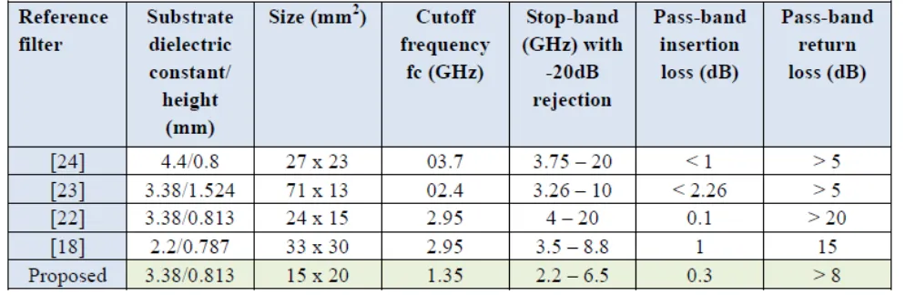
wheref0,fc,f20 dB,α20 dBandα3 dBare the attenuation pole frequency, cutoff frequency, 20-dB stopband frequency, attenuation point at 20-dB and attenuation point at 3-dB, respectively. Such topologies are suitable for ISM band (Industry, Scientific and Medical) applications. The performance of the proposed DGS LPF is summarized in Table 1 with other reported LPFs for comparison. It can be seen from Table 1 that the proposed filter provides good performances in stopband rejection and passband insertion loss, and smaller in size (15×20 mm2) than those reported in literature.
Figure 9. The 3D view of the very compact quasi-Yagi DGS LPF using multilayer technique.
Table 1. Comparison of the proposed quasi-Yagi-DGS-LPF with other related LPF.
8. CONCLUSION
In this work, a new quasi-Yagi DGS low-pass filter (LPF) is introduced and investigated. It is shown that the novel filter has a good sharp cutoff frequency response and good performance in both the passband and stopband. The use of the Yagi idea improves the passband and reject band of the filter compared to the filter without Yagi topology. Using the new quasi-Yagi-arms, it becomes easy to control the resonant frequency without using any extra devices, and consequently, the structure becomes very compact. In order to improve the compactness of the proposed filter, a new multilayer technique is used. A comparison between simulation and measurement results confirms the validity of the quasi-Yagi-LPF configuration and design procedure. Based on its good characteristics, the proposed filter will be a strong candidate for applications in various mobile wireless communication systems as well as in microwave area.
ACKNOWLEDGMENT
The authors thank the German Research Foundation (DFG) for financial support, M. Sc. Eng. Sonja Boutejdar, Mehdi Boutejdar, Karim Boutjdir for their assistant and help and Mr. Harald Dempewolf, the lab manager of the Institute for Electronics, Signal Processing and Communication (IIKT) at the University of Magdeburg, Germany, for his support.
REFERENCES
1. Wu, J.-Y., Y.-H. Tseng, and W.-H. Tu, “Design of compact lowpass filter with ultra-wide stopband using thin slots,”Progress In Electromagnetics Research C, Vol. 31, 137–151, 2012.
2. Boutejdar, A., N. M. Eltabit, A. A. Ibrahim, and E. P. Burte, “Design of wide stop band L-band LPF based on DMS-DGS-technique for radar applications,”Hindawi Publishing Corporation International Journal of Microwave Science and Technology, Vol. 2015, Article ID 101602, 7 pages, 2015.
3. Boutejdar, A., A. Rahman, A. Batmanov, A. Omar, and E. Burte, “Miniaturized band-stop filter based on multilayer-technique and new coupled octagonal DGS with interdigital capacitor,”
Microw. Opt. Technol. Lett., Vol. 52, No. 3, 510–514, Mar. 2010.
4. Hong, J. S. and M. J. Lancaster, Microstrip Filters for RF/Microwave Applications, Wiley, New York, 2001.
structure open-loop ring,” Ultra-wideband, Short-pulse Electromagnetics, 191–200, New York, Springer, ISBN 978-0-387-77844-0, 2010.
6. Abdel-Rahman, A., A. K. Verma, A. Boutejdar, and A. S. Omar, “Compact stub type microstrip bandpass filter using defected ground plane,”IEEE Microwave and Wireless Components Letters, Vol. 14, 136–138, 2004.
7. Al Sharkawy, M., A. Boutejdar, F. Alhefnawi, and O. Luxor, “Improvement of compactness of lowpass/bandpass filter using a new electromagnetic coupled crescent defected ground structure (DGS) resonators,”ACES Journal — The Applied Computational Electromagnetics, Vol. 25, No. 9, Jul. 2010.
8. Dal, A., J. S. Park, C. S. Kim, J. Kim,Y, and T. Itoh, “A design of the low-pass filter using the novel microstrip defected ground structure,” IEEE Trans. Microw. Theory Tech., Vol. 49, 86–93, May 2001.
9. Boutejdar, A. M. Makkey, A. Elsherbini, and A. Omar, “Design of compact stop-band extended microstrip low-pass filters by employing mutual-coupled square-shaped defected ground structures,”
Microwave and Optical Technology Letters, Vol. 50, No. 4, 1107–1111, Apr. 2008.
10. Moyra, T., S. K. Parui, and S. Das, “Design of a quasi-elliptic lowpass filter using a new defected ground structure and capacitively loaded microstrip line,” International Journal on Electrical Engineering and Informatics, Vol. 3, No. 1, 61–73, Apr. 2011.
11. Boutejdar, A., A. Batmanov, E. Burte, and A. Omar, “Design of a new bandpass filter with sharp transition band using U-defected ground structure (DGS) and multilayer-technique,” IET Microwave, Antennas and Propagation, Vol. 4, No. 9, 1415–1420, Sep. 2010.
12. Boutejdar, A., W. Abd Ellatif, A. A. Ibrahim, and M. Challal, “A simple transformation from lowpass to bandpass filter using a new quasi-arrow head defected ground structure resonator and gap-J-inverter,” Microwave and Optical Technology Letters, Vol. 58, No. 4, 947–953, Apr. 2016. 13. Tizyi, H., F. Riouch, A. Tribak, A. Najid, and A. Mediavilla Sanchez, “CPW and microstrip
line-fed compact fractal antenna for UWB-RFID applications,” Progress In Electromagnetics Research C, Vol. 65, 201–209, 2016.
14. Boutejdar, A., A. A. Ibrahim, and E. P. Burte, “A compact multiple band-notched planer antenna with enhanced bandwidth using parasitics strip lumped capacitors and DGS-technique,”
Telkomnika Idonesian Journal of Electrical Engineering, Vol. 13, No. 2, 2015.
15. Han, Y.-L., Y.-C. Jiao, T. Ni, and Z.-B. Weng, “Novel compact dual-band branch-line couplers with half elliptical-ring impedance stub lines,” Progress In Electromagnetics Research Letters, Vol. 56, 9–15, 2015.
16. Wang, X., Z. Ma, I. Sakagami, A. Mase, and M. Yoshikawa, “A small wilkinson power divider with complex isolation component,” Microwave and Optical Technology Letters, Vol. 58, No. 9, 2163–2168, Sep. 2016.
17. Heungjae C., Y. Jeong, J. S. Kenney, and C. D. Kim, “dual-band feedforward linear power amplifier for digital cellular and IMT-2000 basestation,”Microwave and Optical Technology Letters, Vol. 51, No. 4, 922–926, Apr. 2009.
18. Mohra, A. S., “compact lowpass filter with sharp transition band based on defected ground structures,”Progress In Electromagnetics Research Letters, Vol. 8, 83–92, 2009.
19. Boutejdar, A., et al., “DGS resonators form compact filters,”Microwaves and RF, Mar. 24, 2015. 20. Chen, J., Z.-B. Weng, Y.-C. Jiao, and F.-S. Zhang, “Lowpass filter design of hilbert curve ring
defected ground structure,”Progress In Electromagnetics Research, Vol. 70, 269–280, 2007. 21. Boutejdar, A., A. Omar, and E. Burte, “Miniaturized lowpass and bandstop filters using controlled
coupling of open-loop-ring defected ground structure (DGS),” Microwave and Optical Technology Letters, Vol. 52, No. 11, 2575–2578, Nov. 25, 2010.
23. Ting, S. W., K. W. Tam, and R. P. Martins, “Miniaturized microstrip lowpass filter with wide stop-band using double equilateral U-shaped defected ground structure,”IEEE Microwave Wireless Compon Lett., Vol. 16, 240–242, May 2006.
24. Hsiao, P. Y. and R. M. Weng, “An ultra-wide stop-band low-pass filter using dual reverse U-shaped DGS,” Microwave and Optical Technology Letters, Vol. 50, No. 11, 2783–2780, Nov. 2008.