Design and Implementation of Low Power
Phase Lock Loop Using Sense Amplifier
Anurag Bhatt, Gajendra Sujediya
M. Tech. VLSI Scholar, RIET Jaipur, India
Assistant Professor, RIET Jaipur, India
ABSTRACT: PLL with redesigning of individual blocks like- PFD is designed using edge triggered D flip flop to reduce area and static phase error, CP is designed using current mirrored structure to minimize the current mismatch with increased output voltage and VCO has been designed using self bias differential ring oscillator to achieve low jitter operation of PLL. The PLL is designed using 180 nm CMOS technology for high performance with 1.0 V power supply
I. INTRODUCTION
PLL is simple feedback system that compares the output phase with the input phase and produces the output frequency which is proportional to the input phase difference. Since its invention in1932, the basic phase locked loop has remained nearly the same but its implementation in different technologies and for different applications continues to challenge designers. A PLL serving the task of clock generation in a microprocessor appears quite similar to a frequency synthesizer used in a cell phone.
PLL is used to recover a signal from a noisy communication channel, generate stable frequencies or distribute clock timing pulses in microprocessors. The PLL based frequency synthesizer plays a very significant role in direct frequency modulator, frequency demodulator and the regeneration of the carrier from the input signal in the wireless communications. PLL is used for clock and data recovery circuit in the broadband data communication network, which is used to recover the data from the NRZ clock and data re-timed decision.
Phase lock loop design
II. BASIC PLL CIRCUIT
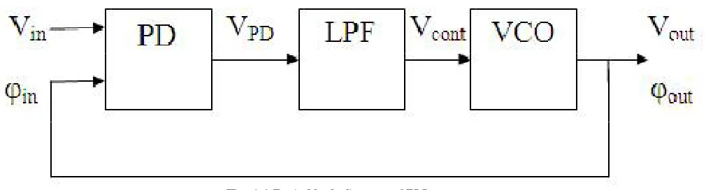
A PLL is a feedback system that compares the output phase with the input phase. The comparison is performed by a ‘phase comparator’ or ‘phase detector’. The basic elements of a Phase locked Loop (PLL) are a Phase detector (PD), Low Pass Filter (LPF) and a voltage controlled oscillator (VCO) in a feedback loop.
Fig. 3.1 shows the basic block diagram of PLL.
Fig. 1.1 Basic block diagram of PLL
Design and implementation PLL
A phase locked loop is a closed loop system that causes one system to track with another. The designing of PLL is done using tanner tool with 1.0 V power supply. The PLL is used for frequency synthesis application in this dissertation, so the block diagram will be taken as frequency synthesizer. Thus the basic block of PLL consists of five fundamental blocks, namely, PFD, CP, LPF, VCO and FD. The proposed PLL is designed to achieve the following properties . Reduced locking time
. Low power dissipation . Delay reduction
. Transistor Count
These design criteria are often I conflicts and improving one particular aspect of the design constrains the other. So each sub block of PLL has been designed in this chapter to satisfy all these properties.
Differential Charge Pump
Differential state is less sensitive to the leakage current and its output voltage is higher than basic charge pump but lesser then supply voltage so the purpose of using the charge pump is not solved. This differential charge pump suffers from some other drawbacks also like higher power dissipation because of two current sources, delay problem due to inverted input, current mismatch problem.
Voltage Controlled Oscillator
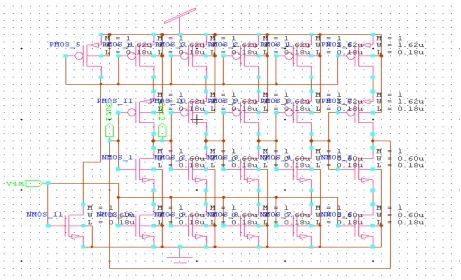
The voltage controlled oscillator is used to generate a specific frequency signal. This VCO is designed using self bias differential ring oscillator as shown in figure 4.11. In this figure, the MOSFETs M2 and M3 operate as inverter while MOSFETs M1 and M4 operate as current sources. The current sources limit the current available to the inverter or it can be said that the inverter is starved for the current. So this type of oscillator is called current starved VCO.
Fig. 1.3 Schematic design of ring voltage controlled oscillator
Here the drain currents of MOSFETs M5 and M6 are the same and are set by the input control voltage. The other transistors M7 to M22 are added just to form the 5-Stages of ring oscillator because it gives better VCO characteristic and frequency range.
. Phase Locked Loop using Sense Amplifier
In this dissertation the PLL is designed using sense amplifier, so the sub blocks used are PFD, CLSA, LPF, VCO and FD. By using the combination of all above sub blocks a PLL is designed as shown in figure 1.4.
Fig.1.4 Schematic design of PLL using sense amplifier
simulation result and analysis
Proposed Phase Locked Loop usingSense Amplifier
The second order PLL using sense amplifier gives locking time of 0.49 µs. The simulation waveform of second order PLL using sense amplifier as shown in figure
.
IV. CONCLUSION AND FUTURE WORK
CONCLUSION
The present work studies the important charge pump and PLL architectures and their performance. In this project, a high speed CMOS sense amplifier for PLL application has been designed and simulated using the 180 nm CMOS technology. Thus this project simulates and analyses some of the major reported sense amplifier architectures for fast locking and less transistor count compared with the design of PLL using charge pump.
I feel confident that my design works properly. Furthermore, I have met the specifications as stated in the introduction. However, I have chosen the values such that we have most of the above features satisfactorily.
FUTURE WORKS
Sense locking time of the PLL is reduced by increasing the order of PLL. Therefore the future work of this project is to design third order PLL using sense amplifier.
REFERENCES
[1]. Sanjay Jaiswal, Dheeraj Jain, Kumkum Verma, Swati Kasht, Arushi Somani “Design of Charge Pump for Fast Locking and Low Power PLL” International Journal of Computer Technology and Electronics Engineering (IJCTEE) Volume 2, Issue 6, December 2012.
[2]. Jyoti Gupta, Ankur Sangal Hemlata Verma “High Speed CMOS Charge Pump Circuit for PLL Applications using 90nm CMOS Technology” World Congress on Information and Communication Technologies IEEE pp.346-349, 2011.
[3]. Silin Liu and Yin Shi, “ Fast Locking and High Accurate Current Matching Phase-Locked Loop” IEEE pp. 1136-1139,2008.
[4]. Abishek Mann, Amit Karalkar, Lili He, and Morris Jones, “The Design of A Low-Power Low-Noise Phase Lock Loop” IEEE pp. 528-531,2010. [5]. Seoncheol Kim and Youngsik Kim, “A Fractional-N PLL Frequency Synthesizer Design” IEEE pp. 84-87,2005.
[6]. Kun-Seok Lee, Byeong-Ha Park, Han-il Lee, and Min Jong Yoh, “Phase Frequency Detectors for Fast Frequency Acquisition in Zero-dead-zone CPPLLs for Mobile Communication Systems” IEEE pp. 525-528,2003.
[7]. Won - Hyo Lee, Sung - Dae Lee and Jun - Dong Cho, “A High Speed, Low Power Phase-Frequency Detector and Charge-Pump Circuits for High Frequency Phase Locked Loop” IEICE TRANS FUNDAMENTALS,VOL.E82-A,NO,11 NOVEMBER 1999.
[8]. Silin Liu, Zhikun Hao, Heping rna, Ling Yuan, and Yin Shi, “A Fast-Locking Phase-Locked Loop Using a Seven-State Phase Frequency Detector” IEEE -2008.
[9]. Muhammad Adeel Ansari, Waqar Ahmad, Svante R. Signell, “Single Clock Charge Pump Designed in 0.35μm Technology” MIXDES 2011,
18th International Conference "Mixed Design of Integrated Circuits and Systems", June 16-18, 2011, Gliwice, Poland.
[10]. Mohammad Sadegh Jalali, Alireza Sharif Bakhtiar, Shahriar Mirabbasi, “A Hybrid Phase-Locked Loop for CDR Applications” IEEE pp. 2533-2536,2011.
[11]. Vahideh Sadat Sadeghi, Hossein Miar Naimi, “A Fast Synthesizer Using a Bang-Bang Frequency Comparator and Locking Status Indicator” 2011 International Conference on Electrical Engineering and Informatics 17-19 July 2011, Bandung, Indonesia.
[12]. Y. Chen, P.-I. Mak and Y. Zhou, “Self-tracking charge pump for fast-locking PLL” ELECTRONICS LETTERS 27th May 2010 Vol. 46 No. 11. [13]. Geum-Young Tak, Seok-Bong Hyun, Tae Young Kang, Byoung Gun Choi, and Seong Su Park, “A 6.3–9-GHz CMOS Fast Settling PLL for MB-OFDM UWB Applications” IEEE JOURNAL OF SOLID-STATE CIRCUITS, VOL. 40, NO. 8, AUGUST 2005.
[14]. A. Djemouai,'M. Sawan,“Fast-Locking Low- Jitter Integrated CMOS Phase-Locked Loop” IEEE 2001.
[15]. Min-Chin Lee, Ming-Chia Hsieh, Ya-Ciou Lin, “Design and implementation of charge-pump phase-locked loop” IEEE 2011 pp. 79-83. [16]. In Ho Hwang, Byung Min Lee and Jong Hwa Lee, “High Performance CMOS Phase Locked Loop For Ubiquitous Network 800MHz ISM Band” 8th INTERNATIONAL WORKSHOP AND TUTORIALS EDM’2007, SESSION IV, JULY 1-5, ERLAGOL pp. 171-173.
[17]. Chun-Pang Wu, Member, IEEE, Sheng-Sian Wang, Member, Hen-Wai Tsao, “A 300KHz Bandwidth 3.9GHz 0.18μm CMOS Fractional-N Synthesizer with 13dB Broadband Phase Noise Reduction” IEEE 2011 pp. 451-454.
[18]. Jianjun Wei, Xinzhang Jia, “Two-Stage Phase/Frequency Detecting CPPLL” 2007 Australasian Telecommunication Networks and Applications Conference December 2nd – 5th 2007, Christchurch, New Zealand, IEEE 2007 pp. 303-306.
[19]. Yau, J., Tu, S.H. “A high-speed frequency acquisition PLL using phase frequency detector with variable gain” IEEE Aug 2010 pp. 101-104. [20]. Nakamura, M.,Yamagishi, A., Harada, M., Kishine, K., “Fast-acquisition PLL using fully digital natural-frequency-switching technique” IEEE Feb 2008 pp. 267-268.