Dept. of Electronics and Communication Engineering, Delhi Technological University, Delhi, India
NEETA PANDEY
Dept. of Electronics and Communication Engineering, Delhi Technological University, Delhi, India
ASOK BHATTACHARYYA
Dept. of Electronics and Communication Engineering, Delhi Technological University, Delhi, India Abstract :
A low delay and speed efficient current mode Analog to Digital Converter has been implemented. The Analog to digital converter architecture generates 4-bit digital output in two stages. Different current comparator architectures have been used in the implementation and for each, the effect on the speed and area of the Analog to digital converter has been determined. It has been implemented using 0.18 µm CMOS technology and simulation results have been obtained using PSpice. The Analog to Digital Converter (ADC) implemented here for 4-bits is expandable for higher number of bits.
Keywords: ADC; current-mode; current comparators.
1. Introduction
With the ever increasing demand of real time signal processing more importance is being given to the circuits responsible for interfacing with real world signals. The real world signals are all analog in nature. The digital signals and digital circuits offer greater advantages as compared to analog circuits in processing speed and efficient transmitting. So in order to convert the analog signals to digital efficiently an Analog to digital converter (ADC) is required.
Current-mode ADCs are gaining popularity owing to the numerous advantages they offer as compared to the voltage mode ADCs. The circuits implemented in current mode technique occupy small area, consume less power and less dynamic range and achieve higher operating speeds. Thus the current mode circuit design methodology has received increasing interest in the past decades [1]-[3].
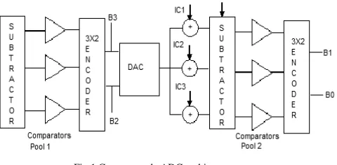
Fig.1 Current-mode ADC architecture
The circuit employs a current comparator. We have implemented the different current comparators suitable for this architecture, each of which has been evaluated in terms of delay and area occupied and hence their effect on the area and speed of the overall ADC design. The ADC also uses an encoder, which we have self designed using CMOS logic implementation of complex digital functions. It offers negligible delay and further adds to the high speed data conversion process. The ADC also uses a current subtractor and Digital to Analog converter (DAC).
The paper has been divided into 3 sections. Section II describes the ADC process. Section III describes each of the blocks used in the ADC and finally Section IV summarizes the simulation results.
2. ADC Process
Fig. 1 shows the block diagram of the implemented ADC. The input to the ADC is a continuously varying current signal in the range described by {min, max}. Using these min and max values, the whole range is divided into many steps, which are considered as the references for comparing the incoming input signal to obtain the digital output. Thus, the step size for n bits at the output is calculated as:
(max min)
(2
1)
xth
n
For our implementation, we have taken the input current signal in range of 0µA to 7.5µA, thus providing reference values of 0.5µA, 1.0µA, 1.5µA,……,7.5µA.
The ADC uses 2 stages, each stage for generating 2-bits in parallel. In stage-I input current Iin is compared with reference currents Irefi (i=1,2,3) by three current comparator, to generate a logic-1 if Irefi < Iin or a logic-0 when Irefi > Iin. These logics so generated are then taken up by an encoder to provide most significant bits B3 and B2 as per the implemented logic.
At stage-II, B3 and B2 are first converted to their corresponding threshold analog current values using a DAC. The two currents are added and replicated to have three currents of same value, say the total reference current value (IDAC). To this total reference current value, a constant current Iconsti (i=1,2,3) is added so that three reference currents are available for current comparison in stage-II. Thus in stage-II, Iin and IDAC + Iconsti are compared in a manner similar to the one in stage-I. The outputs are then encoded and finally the remaining two Least Significant Bits, B1 and B0 are obtained.
3. ADC Modules
The following is a brief description of the individual modules used in the ADC:
3.1.Current Subtractor
The ADC requires a current subtractor to generate the difference of input current and a reference current, which is then fed to the current comparator. There are numerous architectures available for subtractor circuits [3]-[4] used in conjunction with the current comparators. Most of them employ current mirror circuits as their central part for obtaining difference output of the input and the reference current at one of its port.
generated by the output current is used conveniently to indicate the result of the comparison. The comparison process is relatively simple, but the implementation of the current comparator is not as easy. Low input impedance, which is required by current mode circuits, should be considered first. Secondly, a quick time response is demanded by the current comparator.
The main limitation to the time response usually comes from the initial balance of the output branches that often leads to the triode region for some output transistors. Finally, accuracy is very important for comparator, and it depends on the offset caused by the mismatch of transistors. Many good implementations have been reported in the past decades [4]-[13], many of them emphasize on one or several aspects as a trade off against the other characteristics.
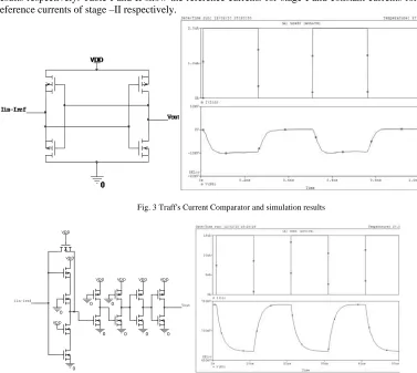
The first CMOS current comparator was proposed by D. Freitas and K. Current in [5]. Since then, many high performance current comparators have been proposed. H. Traff presented a simple and high-speed current comparator in [6], but the output swing of Traff’s comparator could not reach the power supply rails. Many improvements to Traff’s structure have since been proposed in [7]-[12].
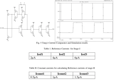
For our implementation, we have chosen the current comparators proposed by Traff in [6], Chen in [8] and Tang in [10]. Figs 3, 4 and 5 show the Traff’s, Chen’s and Tang’s current comparators and their simulation results respectively. Table I and II show the reference currents for stage-I and constant currents for calculating reference currents of stage –II respectively.
Fig. 3 Traff's Current Comparator and simulation results
VDD
0
VDD
0
VDD
0
VDD
0 0
Vout
0
0
0
VDD VDD
Iin-Iref
VDD
Fig. 5 Tang's Current Comparator and Simulation results
Table 1. Reference Currents for Stage-I
Iref1 Iref2 Iref3 2µA 4µA 6µA
Table II. Constant currents for calculating Reference currents of stage-II
Iconst1 Iconst2 Iconst3 0.5µA 1µA 1.5µA
The simulation results show that the worst case delay offered by Traff’s is 0.5ns, Chen’s is 0.42ns and that of Tang’s is 0.252ns.
3.2. Encoder
The implemented ADC requires two 3X2 encoders to convert the 3 outputs obtained from the current comparator pools of each stage into 2-bit digital output. The encoder has been implemented using CMOS technology as described in [13]. The following relation has been used to implement the encoder.
Fig. 6 shows the circuit diagram and simulation results of the CMOS based encoder designed for implementation in this ADC. The encoder introduces a delay of 0.55ns.
C1
0 0
0
B3/B1
VDD
C2
VDD
C3
B2/B0
VDD
Fig. 6 CMOS based Encoder and its simulation results
3.3. DAC (Digital to Analog Converter)
The DAC in the implemented ADC circuit is used to obtain the currents corresponding to the bits B3 and B2 obtained after stage-I. These two currents are combined together as IDAC which is used for obtaining reference currents for stage-II. This is achieved by adding constant currents 0.5µA, 1.0µA and 1.5µA to IDAC by wired addition at a node.
Similarly, the total transistor count for 1-bit conversion is calculated as-
Transistor count of (2*comparators + 2*encoder + DAC + current subtractor)
Based on the above relations the delay and transistor count for ADC using different current comparator architectures is summarized in the Table III below.
Table III. Summary of results for different current comparator architectures
Architecture Total Delay Transistor Count
Traff 5.269ns 45
Chen 5.10ns 53
Tang 4.833ns 65
Table 3 shows that Tang’s current comparator introduces the minimum propagation delay at its output. However, it occupies the largest area thus increasing the overall transistor count and hence increasing the total area at the cost of speed. Traff’s current comparator on the other hand introduces the maximum delay but compensates in terms of the total transistor count. Chen’s current comparator performance and transistor count is in between those of Traff’s and Tang’s. So, based upon the application and the design requirement, a suitable architecture of choice may be employed for the design of this current mode ADC.
5. Conclusion
A 4-bit current mode ADC has been implemented in 0.18 µm CMOS technology. The ADC has been designed using different current comparators, namely Traff’s, Chen’s and Tang’s. All three of these current comparators have been simulated and their delays and total transistor counts have been calculated. The relative comparison of 1-bit conversion using three architectures reveals that while Tang’s structures gives the fastest response, it also occupies the maximum area while its vice versa for Traff’s structure. Chen’s structure demonstrates an intermediary performance.
References
[1] Dlugosz R; Iniewski K. (2006): Ultra-low Power Current Mode Algorithmic Analog to Digital Converter Implemented in 0.18µm CMOS Technology for Wireless Sensor Networks, in Proceedings of International Conference on Mixed Design of Integrated Circuits and System, pp. 22-24.
[2] Rudy van de Plassche (2003): CMOS Integrated Analog to Digital and Digital to Analog Converters, 2nd ed., Kluwer Academic. [3] Golnar K.: Mitra M.; Majid A. (2009): An Area-Speed Efficient Method for Current Mode Analog to Digital Converters, Proceedings
of 2009 European Conference on Circuit Theory and Design, pp. 213-216.
[4] Khucharoensin S.; Kasemsuwan V. (2004): A 3V robust high-speed low input impedance CMOS current comparator, Proceedings of 2004 The 2004 IEEE Asia-Pacific Conference on Circuits and Systems, pp. 1041–1044.
[5] Freitas O.A.; Current K.W. (1983): CMOS current comparator circuit, Electronics Letters., 19, pp. 695-697.
[6] Traff H. (1992): Novel approach to high speed CMOS current comparator, Electronics Letters, Vol. 28, No. 3, pp. 310-312. [7] Banks D.; Toumazou C. (2008): Low-power high-speed current comparator design, Electronics Letters, 44, (3), pp. 171–172. [8] Chen L.; Shi B.; Lu C. (2001): Circuit Design of a High Speed and Low Power CMOS Continuous-time Current Comparator, Analog
Integrated Circuits and Signal Processing, 28, 293–297, Kluwer Academic Publishers, manufactured in The Netherlands. [9] Tang A.T.K.; Toumazou C. (1994): High performance CMOS current comparator, Electronics Letters, 30, (1), pp. 5-6.
[10] Min B.M.; Kim S.W. (1998): High performance CMOS current comparator using resistive feedback network, Electronics Letters, 34, (22), pp. 2074-2076.
[11] Ravezzi L.; Stoppa D. ; Dallabetta G.F. (1997): Simple high-speed CMOS current comparator, Electronics Letters, 33, pp. 1829– 1830.