Effects of Domain Boundaries on the Diffraction
Patterns of One Dimensional Structures
Frederic Timmer1,2and Joachim Wollschläger1,2*
1 Fachbereich Physik, Universität Osnabrück, Barbarastraße 7, 49069 Osnabrück, Germany 2 Center of Physics and Chemistry of New Materials, Barbarastraße 7, 49069 Osnabrück, Germany * Correspondence: [email protected]; Tel.: +49-541-969-2651
Abstract: Motivated by diffraction experiments on the2√3 × √3 R30◦reconstructed Si(111) due to deposition of rare earth elements (Dy, Tb) and silicide formation we analyse the splitting and non-splitting of superstructure spots. For this purpose, we model diffraction patterns for one dimensional structures generated by the binary surface technique and use supercell models to keep the analysis simple. Diffraction pattern are calculated in the framework of the kinematical diffraction theory and they are analyzed as a function of the domains and domain boundaries. Basic properties of the diffraction pattern are analyzed for model systems of a two-fold and a three-fold periodicity. The rules derived from these calculations are applied to the "real-world" system of Si(111)-(2√3 × √3 R30◦)-RESi2(RE = Dy or Tb). Depending on the combination of domains and
domain boundaries of different types a plethora of different features are observed in the diffraction patterns. These are analyzed to determine the sizes of both domain boundaries and domains from experimentally observed splitting of specific superstructure spots.
Keywords: spot-profile analysis; one dimensional physics; low energy electron diffraction; binary surface technique; supercell model; domain boundary
1. Introduction
Many surfaces exhibit superstructures formed to minimize their surface energy. Superstructures are also often formed after deposition of adlayers in the submonolayer regime or even beyond. However, these superstructures often show defects as point defects, e.g., vacancies, or line defects, e.g., domain boundaries. Therefore, it is important to characterize the defect structure of these surfaces. Here, Scanning Tunneling Microscopy is a powerful tool to study locally point and line defects while diffraction can be used to obtain insight in the defect structure on a global scale.
For instance, Low Energy Electron Diffraction (LEED) is an extremely well-suited technique for analyzing the structure of crystal surfaces as well as epitaxial films due to the very high surface sensitivity of electrons. The diffractionpatternis regularly used to obtain first insight in the geometric arrangement and structure of the surfaces. Recording theintensityof the diffraction spots as a function of electron energy (e.g. quantitative LEED) it is even possible to determine the atomic structure of the unit cell down to the sub-Å regime [1–3]. On one hand, dynamical diffraction theory (multiple scattering) needs to be applied here making this approach infeasible for structural analysis of large unit cells (i.e. many atoms) or - even worse - inherent "randomness" (e.g., domain boundaries, atomic steps and other defects). On the other hand, it has been demonstrated that distribution of defects (e.g. domain size distribution, roughness, domain boundaries etc.) can be obtained fromspot profile analysis
(SPA-LEED) in order to learn about the morphology of surfaces [4–7] . This analysis is performed by applying diffraction theory in the kinematic approximation. Accordingly, it is also easily available for large unit cells.
well as semiconductor surfaces [10]. Spot splitting due to the formation of DBs has also been reported for metal covered Si(111) surfaces, e.g., Pb/Si(111) [11,12]. Here, the formation of striped domains and distinct DBs has been deduced from the splitting of√3 × √3 R30◦superstructure diffraction peaks. Streaked superstrucutre diffraction peaks, however, can be attributed to quasi one-dimensional structures where atomic wires (domain size one) are separated by DBs [13].
In this work we investigate the influence of DBs on the splitting of superstructure peaks. For this purpose, we use the supercell approach combined with the binary surface technique. We demonstrate that the splitting or non-splitting of various superstructure peaks has to be taken into account to determine the correct structure of involved DBs. In addition, we apply our results to analyze the complex structure of 2√3 × √3 R30◦ reconstructed Si(111) surface due to rare earth silicide formation where several layers are involved in the formation of the superstructure [14].
2. Results and Discussion
2.1. Methodology
In principle, the intensity of LEED peaks can only be calculated within the full dynamical diffraction theory taking into account multiple scattering effects [1–3]. This technique has been successfully applied in the field of surface crystallography assuming perfectly arranged surfaces without defects.
In the following, however, we will study the effect of domain boundaries on the diffraction pattern of surfaces with superstructures analyzing diffraction spots in the frame of the kinematic diffraction theory. Therefore, the surface is divided in domains with perfectly arranged unit cells and domain boundaries. It has been demonstrated that it is appropriate for defective surfaces to use the kinematic diffraction theory if one considers only diffractionprofiles [4–6]. Here, the scattering from one superstructure unit cell within a domain is integrated into an effective formfactorFSS(E)
(column approximation) whereEdenotes the electron energy. In principle, the same holds true also for the domain boundaries (DB). Thus, we denote the scattering from a unit cell of the DB byFDB(E).
Therefore, the intensity of a diffracted beam
I(H,E) =|FSS(E)
∑
ne2πiHrSS(n)+FDB(E)
∑
me2πiHrDB(m)|2. (1)
assuming a one-dimensional surface for reasons of simplicity. Here, H denotes the scaled lateral scattering vectorH=Kka/2πwith lateral componentKkof the scattering vector and the fundamental
lateral lattice constanta. The intensity depends on both the form factor of the superstructure (SS) as well as the DB unit cellsandon the arrangement of unit cell positions denoted byrSSandrDBfor the
superstructure unit cells and the DB unit cells, respectively. Both positionsrSSandrDBintroduced in eq.(1) are integers due to scaling the lattice constanta.
However, the scattering from the DBs can be neglected for small domain boundary densities. In this case, the diffraction signal is determined from the interference between the different domains separated by DBs and eq.(1) can be simplified:
I(H,E) =|FSS(E)|2|G(H)|2. (2)
where
G(H) =
∑
ne2πiHrSS(n) (3)
G(H) =
∑
nSne2πiHrD(n) (4)
whererD(n)denotes the position of then-th domain (scaled to the lattice constanta) and
S(nD)(H) = Nn−1
∑
n=0e2πiHrss(n) (5)
is the structure factor of then-th domain assuming that this domain consists ofNnunit cells.
2.2. Supercell approach
In the following, we assume that all domains have the same sizeNn ≡ N. Thus, the structure of the surface can be explained by a periodic arrangement of domains of identical sizeNand DBs. Furthermore, the structure factorSn ≡Sis identical for all domains and eq.(5) simplifies to
S(D)(H) = N−1
∑
n=0e2πiH pn= 1−e 2πiH pN
1−e2πiH p (6)
wherepdenotes the periodicity parameter introducing the size of the unit cell of the superstructure
pa. The regular and periodic arrangement of the domains and DBs introduces a length of periodicity
Γa which is equivalent to an effective lattice constant of the supercell. Therefore, the diffraction pattern is described by
|G(H)|2=|S(D)(H)|2
∑
∞ n=−∞δ(H−n/Γ). (7)
Assuming a specific widthwa (w ∈ N) of the DB, the length of periodicity isΓ = N p+w. Thus, diffraction peaks appear in reciprocal space at scaled scattering vectors
Hn = n
N p+w. (8)
Thus, the distance between adjacent diffraction peaks is∆H=1/(N p+w). In addition to the regular pattern of diffraction peaks, the structure factor|S(D)(H)|2emphasizes the regions in reciprocal space
close to diffraction peaks atHn(nom)=n/pexpected for ideal surfaces without any structural defects
as DBs.
2.3. Binary surface technique
Here, we introduce the binary surface technique to treat also surfaces with larger periodicities than surface unit cells [14,15]. Within this approach the crystallographic lattice with the lattice constantais represented by an one dimensional binary array with an array lengthmand with periodic boundary conditions. Consequently,m·a=lcohcorresponds to the coherence length of the diffraction experiment.
Modelling occupied and unoccupied lattice sites by [1] and [0], respecitvely, different periodicities can be modeled. For example, the unit cell of a one-fold periodicity is represented by a simple [1] and the unit cell of a two-fold periodicity can be represented by either [1 0] or [0 1]. Repetitively appending one type of unit cells until the maximum array sizemis reached creates an array/surface with a perfect particular periodicity. For instance, the sequence
[1|1|1|1|1|1|1|1|1|1|1|1]
show a one- and two-fold periodicity for the array lengthm= 12 . By introducing sequences which break this translational symmetry DBs can be modeled. For example, for the surface reconstructed with a two-fold periodicity, this means introducing an additional [1] or [0] between (similar) adjacent unit cells. For instance, the sequence
[10|10|0|10|10|10|10]
depicts the domain boundary [0] in red. Consequently, the surface is now composed of domains reconstructed with the two-fold periodicity separated by DBs.
In this approach, the lattice factorG(H)can simply be calculated as Fourier transform of the binary array. Thus, the binary surface technique is also well-suited to study randomly distributed defects. Here, however, we will solely discuss regular arranged domains of distinct size and DBs while the effect of randomly distributed DBs will be discussed in an other paper [16]. In addition, we will treat here only DBs of the structure [0], [00] etc. for reasons of simplicity.
2.4. Two-fold periodicity
As discussed above, the most simple model for researching the effects of domain boundaries on the diffraction pattern is a surface reconstructed with a two-fold periodicity. Taking a closer look at its possible binary configurations it becomes apparent that it is sufficient to assume one type of domain
D1= [1 0]
and two type of domain boundaries
DB1= [0] or DB2= [0 0].
Fig.1(a) shows the diffraction pattern for a perfect two-fold periodicity (blue). As expected a superstructure peak at H= 1/2, induced by the two-fold periodicity, arises. On one hand, a spot splitting (cyan) of this very peak takes place if DBs of type DB1 (w = 1) are introduced between adjacent domains (here: N=3). As mentioned above, strong diffraction peaks are only observed at positionsHn =n/(2N+1)withn=Nandn= N+1 due to the structure factorS(D)emphasizing diffracton peaks close toH1nom= 1/2. Thus, the spot splitting is∆H=1/(2N+1).
On the other hand, the former superstructure peaks (red) reappears atH1nom = 1/2 if DBs of type DB2 (w = 2) separate domains of two-fold periodicity. Here, the domain boundaries cause the formation of satellite peaks at∆H = ±1/(2N+2)with respect to the original superstructure diffraction peak atH1nom= 1/2.
This very property of spot splitting of the superstructure peak versus satellite formation is equivalent to the observation for atomically stepped surfaces. At out-of-phase diffraction condition
K⊥ =2πn/d, on one hand, one obtains an equally splitted (00) diffraction peak for regularly stepped surface with mono atomic steps due to destructive interference between adjacent terraces of width
Nt (in multiples of the lattice constant a). Here d and K⊥ denote the step height and the vertical scattering vector, respectively. However, it has to be noted that the spot splitting∆Hhere is exactly 1/Ntsince the step height does not contribute since the defect "atomic steps" is perpendicular to the lateral scattering vectorH. In contrast to this, as mentioned above, the width of the DB contributes to the spot splitting due to its lateral character.
Figure 1. (a) Diffraction pattern of the perfect two-fold periodicity (blue) and after introduction of domain boundaries DB1(w= 1, cyan) and DB2(w= 2, red). (b) Diffraction pattern of the three-fold periodicity for theD1domain and the domain boundaries DB1(green), DB2(red), DB3(cyan) and the alternation of DB1and DB2(blue). (c) Diffraction patterns for the alternation of the domainsD1and D2with the domain boundaries DBk= DB1and DBl= DB1(blue), DBk= DB2and DBl= DB2(black), DBk= DB1and DBl= DB2(red) and DBk= DB2and DBl= DB1(magenta)
This out-of-phase and in-phase character of atomic steps can be assigned to the different DBs, too. The spot splitting forDB1is due to destructive interference between adjacent domains while the
sharp peak at the nominal superstructure peak position forDB2is due to constructive interference. Therefore,DB1is an anti-phase domain boundary (APDB) with relative phase shift∆ϕ1=2πw/p= πwhileDB2may be called in-phase domain boundary (IPDB) due to the relative phase shift∆ϕ2 =
2πw/p=2π.
Here, we like to mention that the sharp peak form of all superstructure peaks is caused by our supercellansatz. If the domain widths follow some width distribution these peaks are broadened and the broadening increases with increasing distance to the nominal superstructure diffraction peak at
Hnnom=n/pas will be shown in another contribution [16]. 2.5. Three-fold periodicity
In principle, there are six different types of domains within the binary surface technique for the three-fold reconstructed surface. For reasons of simplicity, however we only consider two domain types in the following:
D1= [1 0 0] and D2= [0 1 0]
DB1= [0], DB2= [0 0] or DB3= [0 0 0].
Thus, most notably the domain boundaries can assume different sizes (w= 1, 2 or 3).
Fig. 1(b) exemplarily shows the diffraction pattern for the domain D1 (here: N = 3) and the domain boundaries DB1 (green), DB2 (red) and DB3 (cyan). Similar to the former result for the
surface with two-fold periodicity we obtain split superstructure spots for short and intermediate DBs, namelyDB1(w= 1,green) andDB2(w= 2, red), respectively. The magnitude of the splitting is equal to the value expected by applying eq.(8). For the long boundary DB3 (w = 3, cyan), however, the superstructure diffraction peak is not splitted but shows satellites separated as expected from eq.(8).
In contrast to the spot splitting for the surface with two-fold periodicity, however, the intensities of both diffraction peaks differ due to different distances to the nominal peak positionHnom=n/3 for the surface without domain boundaries. Therefore, the structure factorS(D)of the domain modifies the intensity of the peaks.
The distances of these peaks with respect to the nominal peak obtained for the defect-free structure either exhibit a ratio of 1:2 or vice versa depending on the sizewof the domain boundary. This can easily be explained within the supercell model considering, e.g., the peaks close toHnom =
1/3. Here, one has to regard the supercell peaksHN andHN+1. For these peaks, the distances∆HN
and∆HN+1with respect toH1(nom)=1/3 are |∆HN+1|
|∆HN| =
3−w
w (9)
which explains the result of|∆HN+1|:|∆HN|= 2:1 forw= 1 and 1:2 forw= 2 independent of the
individual domain sizeNfor the case at hand.
In addition, Fig. 1(b) shows the case of alternation (blue) ofDB1 (w= 1) and DB2 (w= 2) if the type of domainD1(N= 3) does not change. It becomes apparent that in this case the diffraction peaks at the nominal positions (Hnom= 1/3 or 2/3) are still present while additional satellite peaks are created due to the presence of domain boundaries. Due to the alternation of the DBs with different size the next-next-neighbor domains are shifted relatively byw1+w2= 3. Thus next-next-neighbor domains interfere constructively.
This means that there are only two types of phase shifts (∆ϕ1=2π/3,∆ϕ2=4π/3) for adjacent
domains. Consequently, these two domains cannot interfere completely destructively at the nominal position of the perfectly three-fold periodicity and thus the additional peak emerges in the diffraction pattern. Furthermore, the split peaks are now located at equal distances from the nominal position and consequently show a mostly symmetric intensity distribution. This is opposed to the situation for only one type of domain boundary where there are all three types of phase shifts (∆ϕ1 = 2π/3,
∆ϕ2=4π/3 and∆ϕ3=2π) that cancel out each other at the nominal spot position.
This effect for alternating DBs can also be treated in a different way. The sequence
[...|100|100|100|0|100|100|100|00|...]
just discussed can also be rewritten as
[...|100|100|100|010|010|010|000|...]
introducing the domain typeD2combined with theDB3. Thus, the length of periodicity is 2N p+w
As just introduced, not only the domain boundaries can be alternated but the domains themselves as well
[...|D1(N1)|DBk|D2(N2)|DBl|...]
To keep it simple Fig. 1(c) shows onlyD1alternating withD2for every combination of the domain boundariesDB1(w= 1) andDB2(w= 2) with themselves and each other. If both domain boundaries
exhibit equal length (e.g. DBk =DBl =DB1 (w= 1), see fig. 1(c, blue, black)) the magnitude of the
spot splitting decreases to half of the previous value. This reflects the doubled periodicity induced by alternating different domains in addition.
If domain boundaries of different size are alternated, however, an additional effect occurs. If we assume in the following the alternating domains D1 (blue) and D2 (black) as well as domain
boundariesDBk=DB1(w= 1, green) andDBl=DB2(w= 2, red) for example (see fig. 1(c, red)) the following sequence is found in the binary array:
[...|100|100|100|0|010|010|010|00|...].
Alternatively this very sequence can be rewritten by rearranging the domain and domain boundaries:
[...100|100|100|00|100|100|100|0|...].
This means that the two-domain two-domain-boundary model decomposes into an one-domain two-domain-boundary model with the following configuration Di = Dj = D1 (w = 1), DBk = DB2
andDBl =DB2(w= 2). Consequently, the diffraction pattern is analogous to the diffraction pattern depicted in fig.1(b, blue). If we consider the configurationDi=D1(blue),Dj=D2(black),DBk=DB2
(w= 2, green) andDBl=DB1(w= 1, red) (see fig.1(c, magenta))
[...|100|100|100|00|010|010|010|0|...].
you can find the following equivalent expression
[...|100|100|100|000|100|100|100|...],
with identical domainsD1and DBk = DB3(w= 3). This means that the second domain boundary DBl vanishes and the first domain boundaryDBk is commensurable with the three-fold periodicity (e.g. no phase shift) explaining nicely that a quasi-perfect three-fold periodicity can be observed in the diffraction pattern even though domain boundaries are present.
2.6.2√3 × √3 R30◦Reconstruction
In this section the diffraction pattern of the2√3 × √3 R30◦reconstruction of (Dy, Tb) on Si(111) [14] will be discussed as an example demanding a detailed analysis in the framework presented above since the effective unit cells are to large perform standard diffraction.
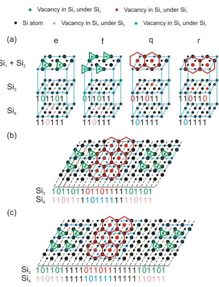
The atomic structure of the reconstruction is rather complex, see fig. 2 as analyzed in [14] combining density functional theory (DFT), scanning tunneling microscopy (STM) and LEED. It is composed of three Si layers. One buckled Si bilayer (Si1, Si2), and two silicene-like (hexagonal,
Figure 2.(a) Schematic display of the structure model of the2√3 × √3 R30◦reconstruction. There are four different energetically favorable models (e, f, q, r) which belong to two different types of domains. The modelseand f make up the first type of domain where the vacancies in the Si3and Si4layer are located underneath Si atoms in the Si2 layer whereas the modelsqandrmake up the second domain where the vacancies in the Si3and Si4layer are located underneath Si atoms in the Si1 layer. Both models exhibit different structural motives in STM measurements [14] which are indicated here by green triangles and red hexagons. The binary sequences after the projection onto the relevant crystallographic axis of the different models for the layer Si3and Si4are given reflecting the fact that the Si3layer exhibits a
√
3×√3 periodicity and the Si4layer exhibits a 2
√
rare earth layers. Experimental evidence shows that the Si3 layer exhibits a √
3 × √3 R30◦
reconstruction and the Si4 layer exhibits a
2√3 × √3 R30◦ reconstruction due to periodically
arranged Si vacancies. The Si4layer has one vacancy per
2√3 × √3 R30◦unit cell while the Si3
has two. Additionally, the vacancies in both layers are not collinearly arranged (cf. colored positions in fig.2).
There is evidence that two different types of domains alternate across the 2√3-direction of the unit cell. Indeed, DFT calculations show that there are four stable structure models (e, f, q,r, see fig. 2) with different arrangements of the vacancies but comparable formation energies. The models (e, f) represent one type of domain D1 and models (q, r) the other type D2. What is more, the
two different types of domains are separated by DBs because a splitting of odd order diffraction spots in 2√3-direction is observed when LEED experiments are performed. Additionally, the DFT calculations predict a tensile strain of the unit cell in 2√3-direction which can only be compensated if no vacancies are assumed for the DBs. Combining all information given above, it can postulated that the spot splitting is explained by a supercell of the following structure
[...|D1(e/f,N1)|DB1|D2(q/r,N2)|DB2|...],
meaning that a domain ofD1(eithereor f) of a size N1alternates with a domain ofD2(eitherqor r) of a sizeN2. Additionally, the two types of domains are separated by DBs where a transition from
one type of domain to the other (D1→D2) does not necessarily have to be the same as the reversed transition (D2→D1) resulting in two different domain boundaries DB1and DB2.
However, experimentally neither the width nor the exact orientation of the different types of domains to each other can be determined by STM. Additionally, the size of the supercell (multiple 2√3 unit cells) makes DFT calculations prohibitive. Thus, in order to gain a deeper insight into the arrangement of the two types of domains kinematical diffraction simulations are performed.
Since both the Si bilayer (Si1, Si2) and the rare earth layer exhibit a 1 ×1 reconstruction they
do not contribute to the superstructure diffraction peaks and can consequently be ignored for their analysis. The two dimensional atomic structure of the√3 × √3 R30◦reconstructed Si3layer and
the2√3 × √3 R30◦reconstructed Si4 layer can be transformed into one dimensional structures
by projecting them onto the crystallographic axis of the 2√3-direction, see fig. 2, in which the two types of different domains (separated by DB) alternate. However, in order to be able to account for the different positions of the vacancies in the unit cell for both types of domains the lattice constant a must be chosen equal to the lateral distance between Si atoms rows in Si(111), i.e. a =a0√3/3 (with
a0= 3.84). Fig.2shows the sequences of binarizations tp perform these calculations.
In order to generate the general diffraction pattern of this two layered structure the vertical phase shift needs to be taken into account
|G(H,L)|2=
GSi3(H) +GSi4(H)exp(2πL) 2
. (10)
HereG(H,L)is the lattice factor as a function of out-of-plane scattering vectorK⊥= 2πL/d(wheredis the layer spacing), GSi3 and GSi4are the lattice factors (Fourier transforms) of the binary arrays of the
respective layers. However, for the following only calculations for integer values ofLare performed unless mentioned otherwise. Hence the diffraction pattern equates to the absolute square of the sum of both of the Fourier transforms due to constructive interference between domains
|G(H)|2=
GSi3(H) +GSi4(H) 2
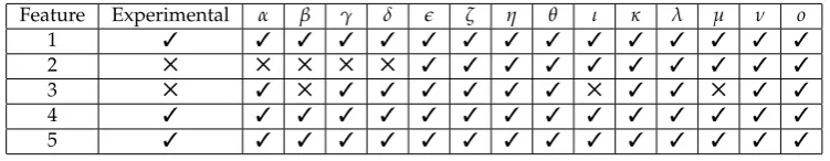
Table 1. Assignment of the 6 features observed in the simulated diffraction patterns (see fig.3(a)) of the 14 models (αthrougho) for the combination of modeleandq.
Feature Experimental α β γ δ e ζ η θ ι κ λ µ ν o
1 3 3 3 3 3 3 3 3 3 3 3 3 3 3 3
2 5 5 5 5 5 3 3 3 3 3 3 3 3 3 3
3 5 3 5 3 3 3 3 3 3 5 3 3 5 3 3
4 3 3 3 3 3 3 3 3 3 3 3 3 3 3 3
5 3 3 3 3 3 3 3 3 3 3 3 3 3 3 3
The simplest way to have D1 and D2 alternate is to alternate only two models which belong to
different types of domains separated by two types of anti-phase domain boundaries creating the following type of supercell
[...|D1(e,N1)|DB1|D2(q,N1)|DB2|...]
In LEED experiments one observes that only peaks of odd order are split(cf. [14]). Therefore, taking into account our previous considerations, it can be deduced that the combined sizew1+w2of the
domain boundary must be an odd multiple ofa0√3 since one would observe a splitting of the even order superstructure spots otherwise. Translated to the binary description this means that the width of the complete domain boundarywtotmust be equal to
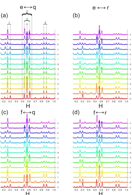
wtot =w(DB1) +w(DB2) =6N+3, N∈N. (12) However, a priori there is no knowledge about the size of the individual domain boundaries. Fig. 3 (a)-(d) shows the diffraction pattern for the coherent superposition of the layers Si3and Si4forN1= N2= 3 andw= 3, 9 for all possible domain boundaries.
In total six different features can be identified in the diffraction patterns. Feature 1 corresponds to the split first order, feature 4 to the second order spot and feature 5 to the split third order spot of the base (2√3 × √3) periodicity and features 2 and 3 can be interpreted as the first order (feature 3) and second order (feature 2) satellites of the second order diffraction spot. Their positions can be explained by the average periodicity of the supercell
Γ=N(D1)2√3+w(DB1)√3/3+N(D2)2√3+w(DB2)√3/3 (13) via eq.8. Tab.1exemplarily shows the assignment of the different features observed in fig.3for the respective models (αthrougho) for the combination of the modelseandq.
Comparing the experimental features to the features observed in the simulated diffraction patterns it becomes obvious that only modelβ(see fig.3(a)) shows the observed diffraction pattern analogous to
the experimental diffraction pattern (only splitting of odd order spots, no additional features). Taking a look at the particular binary configuration for Si3
[...101101|1|011011|011011|011011|11|101101|101101...] [...10110|110110|110110|110110|111|110110|110110|1...]
and Si4
[...110111|1|101111|101111|101111|11|110111|110111...]
it can be found that for this particular arrangement of domain boundaries and domains the binary sequences decomposes into simpler systems. For the Si3layer one receives a
√
3 reconstructed array with only one domain and a commensurate domain boundary explaining a diffraction pattern that is very close to a√3 periodicity. For the Si4 layer one receives a 2
√
3 reconstructed array with a single domain and a domain boundary resulting in a symmetric splitting of (basically only) odd order diffraction spots. For every other combination of domains and domain boundaries only either the binary sequence of layer Si3 or Si4 (or none of them) decompose into a one-domain
one-domain-boundary system. Hence, their diffraction patterns exhibit additional features which are in stark contrast to the experimental findings.
The interference between both layers also plays a significantly role. Due to the lateral displacement of the vacancies in both layers (Si3, Si4) an intensity asymmetry of the first order and
fifth order (split) spots is induced [14].
Analyzing all diffraction patterns of the other combinations of models in the same fashion only one additional model agreeing with the experimental evidence can be found, modelβ(cf. fig.3(d))
for the combination of modelsf andr, which incidentally exhibits the same anti-phase boundaries as for the combination of modelseandq.
This means in order to explain the experimental diffraction pattern only the anti-phase domain boundaries DB1 = [1] and DB2 = [1 1] may be present. Additionally, only transitions from e ↔q
and transitions from f ↔ rmay occur leading to the interpretation that these transitions must be energetically more favorable than the other possible transitions. Having identified the most probable structure of the supercell, its domain size distribution can be determined from the spot splitting∆H. This grants a mean domain sizehγsciof the supercell of
Nsc= N1+w1+N2+w2. (14)
both values are given in unit cells of the 2√3 periodicity, agreeing nicely with the experimental evidence. The analysis can be refined if one take into account domain size distributions to analyze theprofilesof the splitted superstructure spots as presented elsewhere [16].
3. Conclusion
Calculating diffraction patterns and applying the binary surface technique, we were able to show the influence of domain boundaries on the diffraction pattern of the structures. Motivated by the formation of striped domains, these calculatone were performed for one dimensional systems in the framework of the kinematical diffraction theory. Depending on the width of the domain boundaries and combining different types of domains and domain boundaries a plethora of different features can be observed in the diffraction patterns. The analysis of the diffraction pattern obtained from these binary sequences lastly enabled us to identify the structure and width of the domain boundaries of the (2√3 × √3 R30◦) reconstruction of rare-earth silidices (Dy, Tb) on Si(111).
Part of this work has been presented at the international conference on Atomically Controlled Surfaces Interfaces and Nanostructures ACSIN2016 held in Frascati, Rome Italy on Oct 9-15 2016 [17].
Acknowledgments:The authors would like to thank the Deutsche Forschungsgemeinschaft through FOR 1700, project E2, for financial support.
Author Contributions:F.T. and J.W. developed the models, calculated the patterns and wrote the paper.
Abbreviations
The following abbreviations are used in this manuscript:
LEED Low energy electron diffraction
SPA-LEED Spot-profile analysis-Low energy electron diffraction
DB Domain Boundary
APDB Anti-phase domain boundary
SS Superstructure
STM Scanning tunneling microscop DFT Density functional theory
References
1. Pendry, J.B.Low Energy Electron Diffraction; Academic Press: London, United Kingdom, 1974.
2. Van Hove, M.A.; Tong, S.Y.Surface Crystallography by LEED: Theory, Computation and Structural Results; Springer: Berlin, Germany 1979.
3. Clarke, J.L.Surface Crystallography: an Introduction to Low Energy Electron Diffraction; Wiley: Chichester, United Kingdom 1985.
4. Henzler, M. Electron Diffraction and Surface Defect Structure. InElectron Spectroscopy for Surface Analysis; Ibach, H. Ed.; Springer: Berlin, Germany 1977; pp. 117 - 149.
5. Henzler, M. Defects in Surface Structure: Information by LEED. In Festkörperprobleme; Treusch, J. Ed.; Vieweg: Braunschweig, Germany 1979; Volume 19, pp. 193 - 208.
6. Henzler, M. Measurement of Surface Defects by Low-Energy Electron Diffraction. Appl. Phys.,1984,A34 205 - 214.
7. Horn-von Hoegen, M. Growth of semiconductor layers studied by spot profile analysis low energy electron diffractionZ. Kristallogr.,1999,2141 - 75.
8. Altman, M.S. Evidence of a Pb(110) (2×2) reconstruction.Surf. Sci.,1995,34465 - 69.
9. Lizzit, S.; Baraldi, A.; Grütter, Ch.; Bilgram, J.H.; Hofmann, Ph. The surface phase transition and low-temperature phase ofα-Ga(010) studied by SPA-LEED.Surf. Sci.,2009,6033222 - 3226.
10. Iglesias, A.; Gierer, M.; Wolf, D.; Moritz, W. Ordering of subsurface interstitial atoms in the Ge(113) surface studied by SPA-LEED.Surf. Sci.,1999,442357 - 373.
11. Petkova, A.; Wollschläger, J.; Günther, H.-L.; Henzler, M. Formation and commensurate analysis of "incommensurate" superstructures of Pb on Si(111)Surf. Sci.,2001,47111 - 20.
12. Stepanovska, S.; Yakes, M.; Yeh, V.; Hupalo, M.; Tringides, M.C. The denseα-√3 × √3Pb/Si(111) phase: A comprehensive STM and SPA-LEED study on ordering, phase transitions and interactionsSurf. Sci.,2006, 6001417 - 1430.
13. Saranin, A.A:; Lifshitz, V.G.; Bethge, H.; Kayser, R.; Klust, A.; Goldbach, H.; Wollschläger, J.; Henzler; M. Restructuring process of the Si(111) surface upon Ca deposition.Surf. Sci.,2000,44887 - 92.
14. Timmer, F.; Oelke, R.; Dues, C.; Sanna, S.; Schmidt, W.G.; Franz, M.; Appelfeller, S.; Dähne, M.; Wollschläger, J. Strain-induced quasi-one-dimensional rare-earth silicide structures on Si(111).Phys. Rev. B, accepted. 15. Klasing, F.Indium on Silicon(111) Low-energy electron diffraction experiments and simulations on the striped (8×
2) surface reconstruction and the (4×1)↔(8×2) phase-transition, PhD thesis, Duisburg-Essen 2014. 16. Timmer, F.; Wollschläger, J. to be published.
17. A. Acun et al. Atomically Controlled Surfaces Interfaces and Nanostructures”, Bianconi, A.; Marcelli, A. Eds. (Superstripes Press: Rome, Italy 2016
c