6
I
January 2018
Digital control of Active Power Factor Correction
using SPWM Technique
P. P. Mane1, A. D. Shiralkar2
1,2
AISSMS’S Institute of Information Technology {Department of Electrical Engineering}1,2
Abstract: This paper proposes a simple Digital control of PFC using sine pulse width modulation (SPWM) technique. This technique requires DSPIC30F3011, an Inverter circuit & Power factor measurement circuit which detects voltage and current lead/lag. Results of using SPWM give very pure sine wave output with very less harmonics and distortions. The proposed Digital control of PFC is a different approach than boost converter control used in PFC and overcomes the problem of limited switching frequency. The efficiency of the inverter is high and offers very less harmonic distortion. Simulation results indicate that power factor very near to unity can be achieved using the proposed method.
Keywords:PFC, DSP, SPWM.
I. INTRODUCTION
The day by day increase in electronics consumers and the rigid occurrence of mains rectification circuits inside the electronic devices dominants the cause of mains harmonic distortion. Some form of ac to dc power supply are used within the construction of most modern electrical and electronic apparatus and for each half cycle of the supply these supplies take pulses of current. Considering for single apparatus (a domestic television, for example) the amount of reactive power drawn may be small, but for bulk, may be 100 or more TVs the reactive power utilization from the same supply phase causing a flow of substantial amount of reactive current and hence harmonics generation.
[image:2.612.225.427.440.611.2]It is not always the case that the amount of electricity you receive is equivalent to the amount of electricity you use –in fact many on sumers are billed on “wasted” electricity. Customers are liable to pay for the amount supplied even if you aren’t able to utilize all of it. Power Factor is a measure of this inefficiency and Power Factor Correction is the solution used to minimize these inefficiencies.
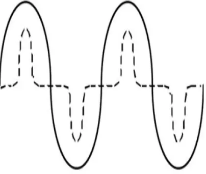
Figure 1: Input of switch mode power supplies without PFC. The voltage waveform is a sine wave and the current waveform is a pulse or spike. PF<1
Figure 2. Voltage and Current waveform s are sinusoidal and in-phase. PF=1
The PF, much like the supply’s efficiency rating, determines the amount of useful power a switch mode power supply can draw from the AC line and then deliver to its output load.
Specifically, the formula that determines this is: VLrms x ILrms x PF x Eff = Pout
As an example, if a power supply is operating off of 120VAC line, which is protected by 15A circuit breaker, UL guidelines say you should not draw more than 12A. So, using the formula above, we can compare two power supply examples with different Power Factors as follows:
Example A : No PFC, PF = 0.65, 85% Efficiency, 120VAC input, 12A max. current: Therefore: 120VAC x 12A x 0.65 x 0.85 = 796 Watts Output Power
Example B : PFC used, PF=0.98, 85% Efficiency, 120VAC input, 12A max. current: Therefore: 120VAC x 12A x 0.98 x 0.85 = 1200 Watts Output Power
As can be seen above, the power supply in Example B (with PFC) can deliver 404 Watts or 51% more power to its output load than the non-PFC supply, a significant increase.
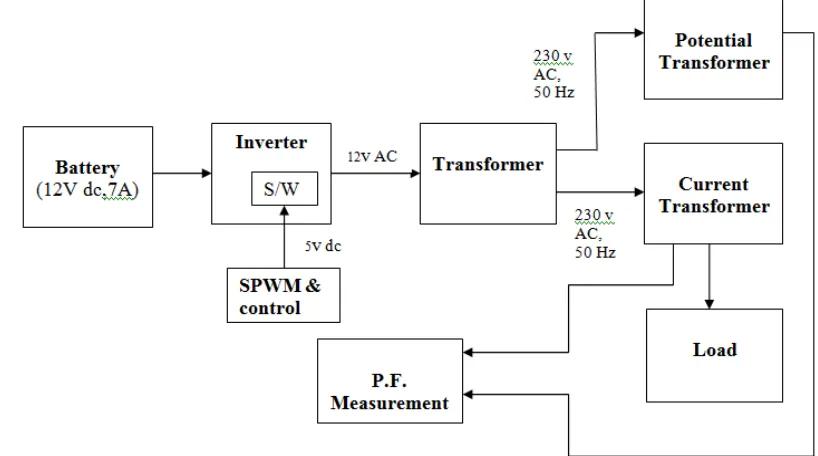
[image:3.612.201.414.85.163.2]II. HARDWAREARCHITECTURE
Figure 3 shows the basic block diagram of Active Power Factor Correction Unit. The components of this APFC unit are Battery for supplying DC voltage to Inverter Circuit, a Transformer which is of Push-Pull type and gives 230V AC output, Switches for switching 5V DC into 12V AC, DSP for SPWM generation and switch control, Potential and Current Transformers along with PIC controller determines Current and Voltage Lead or Lag. Here at the beginning we can use Bridge rectifier to get the 12V DC voltage instead of Battery as a DC source. But, we need to embed a big step down transformer after 230V AC supply which is costlier approach.
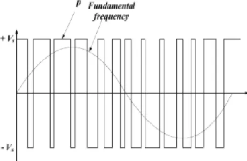
[image:3.612.97.506.482.710.2]III.METHODOLOGY A. Sinusoidal Pulse Width Modulation
To turn the DC voltage on and off, most of the inverters use this PWM technique. This technique generates a DC voltage in a form of pulses of different widths. The width of each pulse is varied as required and hence in a region where you need higher Amplitudes, it will generate pulses of larger widths.
It is one of the PWM method used in Inverters and widely used in Industries. SPWM can be obtained by comparing High frequency Carrier triangular waveform with a Low frequency Sinusoidal waveform, which is nothing but reference or modulating signal. So, by comparing a sine wave with a high frequency triangular wave the On and Off instances of a PWM signal can be determined. In Sinusoidal pulse width modulation, the frequency of Output Voltage is determined by the Frequency of Sine wave or Modulating wave. Also, Modulating waves peak Amplitude determines the modulation index and in terms controls the out voltage rms value. In figure below, we can see “p” pulses. Throughout the cycle widths of these pulses vary to give fundamental component of Frequency.
Figure 4. Sinusoidal PWM signal
B. SPWM Implementation using DSPIC30F3011
DSP has it’s in-built Oscillator which can produce high frequency signals.
In SPWM method, by comparing Sinusoidal reference signal with Triangular Carrier wave frequency, the gating signal is generated. By varying the width of each pulse in proportion to the amplitude of the reference wave we can achieve following major advantages The distortion factor and lower order harmonics can be reduced significantly.
The width of all the pulses are maintained the same. This type of modulation is known as Sinusoidal Pulse Width Modulation. By comparing sinusoidal reference signal with a triangular carrier wave of frequency, the gating signal is generated.
IV.HARDWAREDEVELOPMENT&RESULTS
A. Inverter Circuit & DSP Output
It consists of one PWM modulator SG3524 and 2 MOSFET switches. For SG3524, we are giving 9V DC regulated output and we get a 5V DC, 50Hz little distorted square wave as its output. DSPIC30F3011 compares carrier triangular wave with sinusoidal reference signal generates two SPWM signals which are opposite to each other using NOT logic gate inside it. These two SPWM Signals are of very high frequency in Khz but with pure square wave of 5V DC signal.
[image:4.612.185.429.251.410.2]B. Push-Pull Transformer
[image:5.612.205.420.160.276.2]The Basic theory is as follows: The top transistor switch closes and causes current to flow from the battery negative through the transformer primary to the battery positive. This induces a voltage in the secondary side of the transformer that is equal to the battery voltage times the turns ratio of the transformer. Note: Only one switch at a time is closed. (See state Figure 5 below). After, certain desired period the switches flip-flop. The top switch opens and then the bottom switch closes allowing current to flow in the opposite direction (See state Figure 6 below). This cycle continues and higher voltage AC power is the result.
Figure 5. Push-Pull Topology – Square wave output
Figure 6. Push-Pull Working with Switches open and closed
C. Power Factor Measurement Circuit
We are using Current transformer and Potential Transformer across transformer output and then their output would be connected to Power Factor Measurement Circuit. This measurement circuit consists of PIC microcontroller and LM358 used as ZCD to detect voltage and current lead and lag. This way Power factor is measured and shown on LCD display.
V. SIMULATION &RESULTS
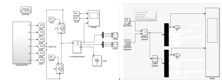
A. Push-Pull Inverter system using SPWM is simulated using MATLAB/SIMULINK
[image:5.612.107.522.308.462.2][image:5.612.114.492.578.715.2]
VI.SIMULATIONRESULTS
Figure 8. Simulation Results- Current and Voltage
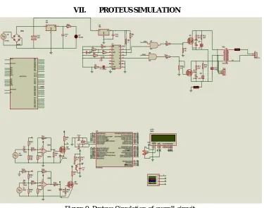
VII. PROTEUSSIMULATION
Figure 9. Proteus Simulation of overall circuit.
The simulation results are matching with actual behavior of system. Same will be used in actual Hardware implementation.
VIII. CONCLUSIONS
With a higher power factor at light load, meeting higher power factor requirement at light load will be possible for power supplies of desktop computers and servers. Moreover, bringing the power factor at light load to be close to unity helps in reducing the rms current drawn from the ac mains. This helps in reducing the power consumption under light load conditions and in meeting the ENERGY STAR light load efficiency requirement.
The prototype has been tested with two different loads (electronic choke coil and 100W tungsten bulb), and the experimental results show, in both cases, high power factor with reliable performance under different load and voltage conditions.
Some of the features of the proposed method for the PFC unit presented in this paper are as follows.
Information on the required signal is obtained via two paired sawtooth waves compared with the sensed signal, without any ADC used.
This scheme doesn’t use traditional boost approach hence reducing complex designing of inductor and also cost effective. There is no ADC required to realize the fully digitalized control of the PFC.
[image:6.612.126.501.218.513.2]REFERENCES
[1] Fully Digitalized Implementation of PFC Rectifier in CCM Without ADC ’’ This paper is published in 2012 by K. I. Hwu, Member, IEEE, H. W. Chen, and Y. T. Yau, Student Member, IEE
[2] In 2014 year A Safari, Colin W. Clark, Member, IEEE, Fariborz Musavi, Senior Member, IEEE, and Wilson Eberle, Member, IEEE, published the paper, ‘‘Digital DCM Detection and Mixed Conduction Mode Control for Boost PFC Converters ’’
[3] A Novel DSP-Based Current-Controlled PWM Strategy for Single Phase Grid Connected Inverters” This paper is published in 2006 by Hossein Madadi Kojabadi, Bin Yu, Idris A. Gadoura, Member, IEEE, Liuchen Chang, Senior Member, IEEE, and Mohsen Ghrib
[4] In 2014 year Alberto Sanchez, Angel de Castro, Member, IEEE, Victor Manuel L´opez, Student Member, IEEE, Francisco J. Azcondo, Senior Member, IEEE, and Javier Garrido, Senior Member, IEEE published the paper, ‘‘Single ADC Digital PFC Controller Using Precalculated Duty Cycles’’
[5] DSP-Based Interleaved Buck Power Factor Corrector With Adaptive Slope Compensation’’ This paper is published in 2015 by Cheng-Yan Yang, Student Member, IEEE, Chen Liu, Student Member, IEEE, Po-Jung Tseng, Student Member, IEEE, Tian-Fu Pan, Huang-Jen Chiu, Senior Member, IEEE, and Yu-Kang Lo, Member, IEEE
[6] Digital Control for Improved Efficiency and Reduced Harmonic Distortion Over Wide Load Range in Boost PFC Rectifiers” this paper was published in 2010 by Fu-Zen Chen and Dragan Maksimovi´c, Senior Member, IEE
[7] Switching Power Supply Design Third Edition” by Abraham I. Pressman, Keith Billings, Taylor More
[8] “ Application Note AN-53” – “ Active Power Factor [9] “The Art of Electronics” by Paul Horowitz, Winfield Hil [9] Fundamentals of Power Electronics” R. W. Erickso
[10] “Practical switching Power supply design” by Marrty Brow