'
Applied Mechanics and Materials Vols. 465-466 (2014) pp 916-921 O (2014) Trans Tech Publications, Switzerland
' doi:10.4028/www.scient~c.net/AMM.465-466.916
Fabrication of Multilayer ZnOlTi021Zn0 Thin Films with Enhancement of
Optical Properties by Atomic Layer Deposition (ALD)
Rosniza
us sin",
Kwang-Leong choJb and Xianghui
HOU~''~epartment of Materials Engineering and Design, Faculty of Mechanical and Manufacturing
Engineering,Universiti Tun Hussein Onn Malaysia (UTHM),86400 Pant Raja, Batu Pahat, Johor, Malaysia
2
Faculty of Engineering, Department of Mechanical, Materials and Manufacturing Engineering, University of Nottingham NG7 2RD, United Kingdom.
Keywords: Atomic Layer Deposition, Thin films, Zinc Oxide, Titanium oxide, bilayer ZnO/TiOn, Multilayer ZnO/Ti02/Zn0, Transmittance
Abstract. Atomic layer deposition (ALD) is a precision growth technique that is able to deposit either amorphous or epitaxial layer on a wide range of substrates. Multilayer thin films have been widely studied because their properties are different fiom those of bulk materials constituents owing
to the two-dimensional films and high density of interfaces. Multilayer nanostructured thin films
were fabricated on silicon and glass substrates by ALD. The optical and electrical of multilayer ZnO/Ti02/Zn0 films were investigated. The microstructure compositions and surface morphology
of these multilayer films were analyzed by X-ray diffraction (XRD), Atomic force microscope
(AFPVI) and Scanning electron microscope (SEM). The optical properties were characterized using
photoluminescence (PL) and W-VIS spectroscopy. XRD patterns confirmed that ZnO with
wutrtize crystal structure and Ti02 with anatase structure were presented. The degree of crystallinity of multilayer thin films has been improved through the deposition of ZnO. The intensity of W luminescence of the multilayer has increased as compared to the single layer Ti02 and bilayer ZnO/Ti02. The multilayer ZnO/Ti02/Zn0 has high transmittance (above 80%) in visible region. All the result suggested that the use of multilayer thin films effectively enhanced the quality of films crystallinity and optical properties as compared to single layer ZnO and bdayer ZnOITiO2.
Introduction
Multilayer thin films consist of alternating layer of two different materials which may contain several repeated thin films layer in range of nano or micro scale [I]
.
Zinc Oxide (ZnO) based nanostructured composites become more attractive when being simply assemble together with other metallic oxide[2].The growth of transparent conducting oxide (TCO) semiconductor is essential as expending needed for transparent electrode for optoelectronic devices. ZnO thin films have wide applications due to the superior electrical [3-91 and optical properties [3-5, 7, 10, 111. The outside layer can be deposited on the ZnO surface by different deposition method such as electron beam evaporation [12], sputtering system [13], and atomic layer deposition [14,15,16]. Titanium dioxide (Ti02) is a ceramic material with versatile applications for self-cleaning, biocompatible, andcorrosion resistance [17]. The unique microstructure and improved optical and electrical properties
are reported [18-191. The increase in light emission or efficiency enhancement for dye-sensitized
solar cell definitely proves that these trpes of multilayer nanostructures or nanocomposite have enhanced optical and electrical properties that may have functional applications. The high precision
and confomality of ALD process could produce bilayer thin films [15] and multilayer thin films
with controlled thickness and microstructures. However, to the best of our knowledge, there is no
report on multilayer of ZnO/Ti02/Zn0 (ZTZ) thin films by ALD. In this paper we attempt to
synthesize uniform multilayer of ZTZ
thin
films in order to obtain enhanced crystallinity and optical properties of this multilayer.Experimental
ALD was used to deposit multilayer ZTZ on the silicon wafer and glass as substrate. ZnO was deposited at 280°C for 1200 deposition cycles. The process were operated with pulse H20 at 0.15s and diethylzinc (DEZ) at 0.015s pulse rate, pumps at 5s, and nitrogen flow 20 sccm. The sequence of one ALD cycles was H20/N2/DEZ/N2. Then, Ti02 thin films were deposited on ZnO films at 300°C for 2000 cycles. The process were operated with pulse H20 at 0.15s and tetra-iso-propoxide (TTIP) at 0.20s pulse rate, pumps at 5s, and nitrogen flow 20 sccm. The sequence of one ALD cycle was H20/N2/'I"TIP/N2. After that, another ZnO layer was deposited at 280°C for 1000 cycles with same process parameters. The phase and crystallinity of the multilayer films were analysed by X-
ray diffraction (XRD, Siemens Kristalloflex-D500) with Cu-Ka radiation. Eva software was used to analyse the phase. The surface morphology and surface roughness were characterized using Atomic Force Microscope (AFM, Veeco, CPPII-Research scanning probe microscope). ImageJ software was used to determine particle size fiom AFM image. The photoluminescence of the multilayer thin films were measured by Hitachi F-2500 fluorescence spectrometer. The optical transmittance spectra were measured by Biochrom Libra S33 UVNis-spectrometer.
Result and discussion
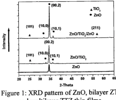
Uniform single layer, bilayer and multilayer thin films were deposited on silicon wafer substrates. Fig 1 shows XRD patterns of ZnO single layer, bilayer of ZnO/Ti02 (ZT) and multilayer ZnO/Ti02/Zn0 (ZTZ). All XRD patterns confirmed that ZnO with wutrtize crystal structure and Ti02 with anatase structure were presented. XRD pattern of ZnO thin film matched with the wurtize structure (JCP 22.2CA 01-079-2205) and Ti02 thin films matched with the anatase structure (JCPDS pattern 00-021-1272). All the peaks of the single layer ZnO deposited using 1200 cycles are in good accordance with the diffraction values of hexagonal wurtzite structure with predominantly (00.2) orientation. Bilayer ZT of thin films shows increases of intensity in orientation (0.02) after the deposition of Ti02. Moreover, the intensity at (0.02) orientation increases for multilayer ZTZ. The sharp peak indicates the multilayer films are well crystallized. It shows that the films crystallinity has been drastically improved with multilayer deposition. The improvement of crystallinity of ZTZ multilayer thin films has also been reported using other techniques [20, 211. The crystallite size calculated using Scherrer formula for ZnO, ZT, and ZTZ were 27.2 nm, 28.26 nrn and 33.7 nm, respectively (Fig 2). The increase of crystallite size indicates that the crystallinity of ZTZ multilayer has been improved.
[image:2.597.126.311.514.673.2]2-Theta 7 TI 7T7
Figure 1 : XRD pattern of ZnO, bilayer ZT Figure 2: RMS and crystallite size and multilaver ZTZ thin films of Z (ZnO),bilayer ZT,and
[image:2.597.338.496.524.690.2]91 8 4th Mechanical and Manufacturing Engineering
[image:3.611.91.486.82.214.2](a) Single ZnO layer films (b) Bilayer ZnO/Ti02 thin films (c) Multilayer ZnO/TiO,/ZnO thin films
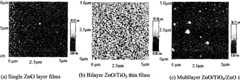
Figure 3: AFM of single ZnO layer, ZT bilayer and ZTZ multilayer films
The morphology of thin films was observed with AFM, together with the assessment of the relative roughness of the thin films (RMS parameter). The morphology fiom AFM image (fig 3) illustrates that bilayer ZT consisted of compact grains which was very similar to the single ZnO layer. However, multilayer ZTZ had much larger grain size compared to the single layer and bilayer. The relative roughness of these thin films was also very close (fig 2). The value of RMS for ZnO, bilayer ZT and multilayer ZTZ were 2.89 nrn, 2.80 nm and 3.17 nm, respectively. Particles sizes, orientation, shapes and distribution play an important role in governing the performance and reliability of polycrystalline films. An evolution of the particles size distribution may occur depended on the deposition temperature and impurities segregated at the grain boundaries [22]. The correlation between the films morphology and its optical properties is complicated. It is depends on grain size, orientation and grain boundaries. A grain boundary is identifying as the interface at which grains move towards and contact with another different crystal orientation. Several kinds of defect are present at grain boundaries such as dangling and impurities [23]. Therefore, multilayer thin films may attribute to the change of particle shapes that contributes to the improvement of crystallinity and optical properties. The crystallinity properties of the films is clearly dependent on the kinetics of arriving species at the surface [23].
The optical properties of thin films were the response of material deposited on the substrates to electromagnetic waves or light waves, principally in the wavelength spectrum of visible light (400-700nm). Figure 4 illustrates the transmittance spectra of ZnO thin films, ZT bilayer thin films and ZTZ multilayer thin films. It shows that multilayer ZTZ have high transmittance (-80%) in
100- . , . ,
.
, . , ,no -
E
0 - - - . , , , , ,
300 400 500 SW 700 BW
Wavelenglh (nrn)
350 400 i o 5bo
[image:4.596.97.501.78.245.2]Wavelength (nm) Figure 4: Transmittance of ZnO, bilayer
Figure 5: PL spectra of ZnO, bilayer ZIT ZT and ZTZ multilayer thin films
and ZTZ multilayer thin films
Fig 5 shows the PL ZnO spectra, ZT bilayer and ZTZ multilayer thin films. The spectra were collected under photon excitation 320 nm using xenon lamp. The PL spectra shown strong and sharp UV emission located around 380 nrn and no other visible light emission peak can be seen, demonstrated of good crystallinity quality of multilayer ZTZ thin films growth by ALD. The near
W emission is attributed to fiee-excition recombination 1241. Compared to the ZnO single layer, the UV emission of the multilayer ZTZ is greatly enhanced. The PL intensity of the UV emission increased with the increase of the crystallite size because of the enhanced crystallinity of thin film. This also may attributed to the higher barrier in valence band which prevents the hole movement [12]. These also agree with the particles size in multilayer. The enhanced the increase of UV
emission can be explained with two reasons: the surface passivation effect due to the capping TiOz particles and the fluorescence resonance energy transfer (FRET) between Ti02 layer and ZnO layer [191-
Conclusion
Uniform multilayer ZTZ thin films have been successfully deposited by ALD. The crystallinity of thin films has been improved with multilayer thin films. The intensity of UV luminescence of multilayer increases as compared to those of the single layer Ti02 and bilayer ZT. It shown that multilayer ZTZ has high optical transmittance (above 80%) in visible region. It is suggested that the growth of multilayer ZTZ thin films enhanced the crystalinity and optical properties. The multilayer thin films show much enhanced the crystallinity and optical propel-ties because of the combination and interaction effect between different metal oxides. These multilayer ZTZ thin filrns can be used to as transparent conductive thin films.
Acknowledgments:
This work was financially supported by the University Tun Hussein Onn Malaysia (UTHM),
Ministry of Higher Education Malaysia and the European Union commission under EU-FP6 EXCELL project.
References
[ l ] C. A. Ross, Electrodeposited multilayer thin films, Anual Review of Materials Science VOL 24 (1 994) pages 1 59
[2] Sun-Woo, Choi, et al., Synthesis of Sn02-ZnO core-shell nanofibers via a novel two-step process and their gas sensing properties, Nanotechnology 20 (2009) 465603.
920 4th Mechanical and Manufacturing Engineering
A. W. Ott, R. P. H. Chang, Atomic layer-controlled growth of transparent conducting ZnO on plastic substrates ,Materials Chemistry and Physics 58 (1 999) 132- 13 8.
E. Przezdziecka, T. Krajewski, L. Wachnicki, A. Szczepanik, A. Wojcik-Glodowska, S. Yatsunenko, E. Lusakowska, W. Paszkowicz, E. Guziewicz, M. Godlewski, Characterization of ZnO Films Grown at Low Temperature, Acta Physica Polonica A 114 (2008) 1303-1310.
S. Kwon, S. Bang, S. Lee, S. Jeon, W. Jeong, H. Kim, S. C. Gong, H. J. Chang, H. H. Park, H. Jeon, Characteristics of the ZnO thin films transistor by atomic layer deposition at various temperatures, Semiconductor Science and Technology 24 (2009) 1-6.
A. Yarnada, B. S. Sang, M. Konagai, Atomic layer deposition of ZnO transparent conducting oxides. Applied Surface Science 1 12 (1 997) 2 16-222.
S. H. K. Park, Y. E. Lee, Controlling preffered orientation of ZnO thin films by Atomic layer deposition, Journal of Materials Science 39 (2004) 2195-21 97.
Sangsang, B. and, Yamada, A. and, Konagai, Makoto, Highly Stable ZnO Thin Films by Atomic Layer Depositions, Japanese journal of applied physics. Pt. 2, Letters 37 (1998) L1125-L1128.
A. Pourret, P. Guyot-Sionnest, J. W. Elam,Atomic Layer deposition of ZnO in Quatum Dot Thin Films, Advanced Materials 21 (2009) 232-235.
Y. H. I. a. Y. B. H. Suk Lee, Two-step growth of ZnO films on silicon by Atomic layer deposition.Korean Journal Chem. Eng 22 (2005) 5.
W. S. Choi, E. J. Kim, S. G. Seong, Y. S. Kim, C. Park, S. H. Hahn, Optical and structural properties of ZnO/Ti02/Zn0 multilayer prepared via electron beam evaporation,Vacuurn 83 (2009) 878-882.
F. Huang, B. Xie, B. Wu, L. Shao, M. Li, H. Wang, Y. Jiang, Y. Song, Enhancing the crystallinity and surface roughness of sputtered Ti02 thin films by ZnO underlayer. Applied Surface Science 255 (2009) 6781-6785.
H. Kumagai, Y. Tanaka, M. Murata, Y. Masuda, T. Shinagawa, Novel Ti02/Zn0 multilayer mirrors at 'water window' wavelengths fabricated by atomic layer epitaxy, Journal of Physics: Condensed Matter 22 (1 December 20 10) 474008-4740 14.
R. Hussin, X. Hou, and K-L Choy, Growth of ZnO Thin Films on Silicon Substrates by Atomic Layer Deposition, Defect and Diffusion Forum, VOL 329, Paper 16,159- 164, (20 12)
R. Hussin, X. Hou, and K-L Choy, Enhancement of Crystallinity and Optical Properties of Bilayer Ti02 /ZnO Thin Films Prepared by Atomic Layer Deposition. Journal. Nanosci. Nanotechnol. VOL 11, Number 9, 8 143-8 147 (20 1 1).
C. X.Shan, X. Hou, K.-L. Choy, C. Patrick, Improvement in corrosion resistance of CrN coated stainless steel by Atomic Layer Deposition, Surface and Coatings Technology 202 (2008) 2147-2151.
L. Xu, L. Shi, X. Li, Effect of Ti02 buffer Layer on the structural and optical properties of ZnO thin films deposited by E-beam evaporation and sol-gel method. Applied Surface
Science 255 (2008) 3230-3234.
L. Xu, H. Shen, X. Li, R. Zhu, Enhanced ultravoilet emission from ZnO thin film covered by nanoparticles, Chin. Opt. Lett. 7 (2009) 953-955.
[21] A. F. Lotus, S. N. Tacastacas, M. J. Pinti, L. A. Britton, N. Stojilovic, R. D. Ramsier, G. G. Chase, Physica E: Low-dimensional Systems and Nanostructures In Press, Corrected Proof.
[22] K. S. S. Harsha, Principles of physical Vapour deposition of thin films, Elsevier Ltd, 2006.
[23] J. P. Kar, G. Bose, S. Tuli, Correlation of electrical and morphological properties of sputtered aluminium nitride films with deposition temperature, Current Applied Physics 6 (2006) 873-876.
[24] U. Choppali, B. P. Gorman, Structural and Optical properties of nanocrystalline ZnO thin films synthesized by the citrate precursor, Journal of Luminescence 128 (2008) 164 1 - 1648.
[25] M. Tadatsugu, Transparent conducting oxide semiconductors for transparent electrodes,
Semiconductor Science and Technology 20 (2005) S35.