© 2017, IRJET | Impact Factor value: 5.181 | ISO 9001:2008 Certified Journal | Page 360
Comparative Study of Voltage source inverter with Z source inverter
Devadkar Supriya
1, Gaikwad Snehal
2, ZagadeNutan
3,Pawar P.B.
4123
Student of S.B.Patil College of Engineering,Indapur
4
Assistant Professor, Dept. of Electrical Engineering, S.B.Patil college of
Engineering,Indapur,Maharastra,India
---***---Abstract -
An implementation of the constant V/Hz
control strategy for proposed impedence source inverter(Z – source inverter)fed induction motorin closed loop control has emerged as a powerful tool for controlling induction motor drives to achieve high performance and good dynamic response. In this paper, a new control scheme is developed for control of the induction motor drive by ZSI by boosting line voltage, lowering harmonics distortion,maintaining speed of the drive. In this scheme stator voltage is boosted for obtaining desired torque response and maintain constant frequency and speed below rated speed. Simulation results of the proposed Z –source inverter scheme and traditional inverter are presented which compared for their comparative study.
Key Words: Z source inverter ,Induction motor drive, Harmonics distortion
1.INTRODUCTION
Nowadays, energy storage and conversion plays the vital role in the field of distributed generation.Many of them uses converter such as rectifier and inverter. This paper reviews some of traditional inverter topology such as current source inverter and voltage source inverter with their drawbacks hence introducing newer topology as z- source inverter which had discuss further.
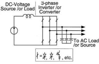
[image:1.595.93.254.553.657.2]1.1 CURRENT SOURCE INVERTER
Fig 1: Current Source Inverter
Fig. 1.shows the traditional three-phase current source inverter structure. A dc current source feeds the main converter circuit, a three-phase bridge. The voltage source such as a battery, fuel-cell stack, diode rectifier, or thyristor inverter provides dc current source fed by the dc inductor. The power transistor such as Insulated Gate Bipolar Transistor (IGBT), Silicon ControlledRectifier
(SCR), Metal Oxide Semiconductor Field Effect Transistor (MOSFET), or a combination of such devices with the series diode is used. These devices act as switching devices according to their switching sequence the three phases AC output was obtain is given to load. For CSI shape of the output voltage is depending on load and output current is independent of load. The CSI is to work as a current source by means of the large series inductor at its output and a current regulation loop.
1.1.1 LIMITATIONS OF CSI:
1. The ac output voltage has to be greater than the original dc voltage that feeds the dc inductor or the dc voltage produced is always smaller than the ac input voltage. There-fore, the current-source inverter is a boost inverter for dc-to-ac power conversion and the current source converter is a buck rectifier (or buck converter) for ac-to-dc power conversion. For applications where a wide voltage range is desirable, an additional dc–dc buck (or boost) converter is needed. The additional power conversion stage increases system cost and lowers efficiency.
2. At least one of the upper devices and one of the lower devices have to be gated on and maintained on at time. Otherwise, an open circuit of the dc inductor would occur and destroy the devices. The open-circuit problem by EMI noise mis-gating-off is a major concern of the inverter’s reliability. Overlap time for safe current commutation has to be required in the current source inverter, which may causes waveform distortion, etc.
3. The main switches of the current source inverter have to block reverse voltage that requires a series diode to be used in combination with speed and high-performance transistors such as insulated gate bipolar transistors (IGBTs).
1.2 . VOLTAGE SOURCE INVERTER:
© 2017, IRJET | Impact Factor value: 5.181 | ISO 9001:2008 Certified Journal | Page 361 Fig 2: Voltage Source Inverter
The capacitorC is connected in series with diode.The power transistors such as Insulated Gate Bipolar Transistor (IGBT), Silicon Controlled Rectifier (SCR), Metal Oxide Semiconductor Field Effect Transistor (MOSFET), or combination of such devices with antiparallel diode is used to provide bidirectional current flow and unidirectional voltage.
The output voltage of VSI is smaller than input voltage which can be supplied by the rectifier, fuel cell,battery, photovoltaic array. It is essential to boost that voltage by DC-DC boost converter which reduces reliability as well as electromagnetic interference probably reduced performance of the inverter.
1.2.1 LIMITATIONS OF VSI :
1. Voltage-source inverter is a buck (step-down) inverter for dc-to-ac power conversion. For applications where over drive is desirable and the available dc voltage is limited, an additional dc-dc boost converter is needed to obtain a desired ac output. The additional power converter stage increases system cost and lowers efficiency.
2. The upper and lower devices of each phase leg cannot be gated on simultaneously either by purpose or by EMI noise. Otherwise, a shoot-through would occur and de-stroy the devices. The shoot-through problem by elec-tromagnetic interference (EMI) noise’s mis gating-on is a major killer to the inverter’s reliability. Dead time to block both upper and lower devices has to be provided in the voltage source inverter, which causes waveform distor-tion, etc.
2. Z-SOURCE INVERTER
:The Z-source inverter consists of rectifier unit, impedance network and inverter circuit with three phases AC Induction motor. The input 3 phase AC supply fed to the Rectifier which converts AC Supply to the DC supply. The output of rectifier DC voltage fed to the impedance network. The impedance network consists of twoinductors and two capacitors with similar value because circuit is symmetry. The inductors are connected in series and capacitor is connected diagonal arm.Due to two identical inductor and two identical capacitors the
circuit has unique feature to avoid short circuitwhen the device are in shoot through mode. The switches used in converter is MOSFET anti parallel with DIODE. The impedance network used to boost or buck voltage depend- upon the boost factor. This network acts as filter. The output of impedance network fed to the inverter which convert DC voltage to the AC voltage and fed to the AC load (AC motor).The voltage source inverter has six active states and the Z-source inverter has one extra zero state. It has nine permissible states.
2.1 ADVANTAGES OF Z-SOURCE INVERTER
The z-source inverter works as either voltage source or current source.
It can be work as Buck-Boost converter. Hence it can give the desired output voltage.
Its reliability is high due to lower EMI noise and harmonics.The ZSI can work on load either be Inductive, Capacitive or Z-source network.
2.2MODES OF OPERATION
:
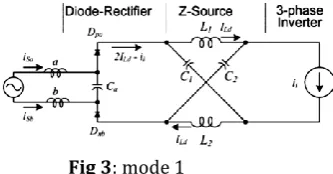
MODE 1:The inverter bridge is operating in one of six traditional active vectors. It acting as current source viewed from the DC link. Both the inductor has same value because circuit is symmetry. Bothinductors carry the current.
Fig 3: mode 1
MODE 2:Theinverter bridge is operating in one two traditional zero vector and shorted through upper or lower two device of inverter via like open circuit from Z-source. In these mode inductor carry current and contribute line current.
Fig 4: mode 2
© 2017, IRJET | Impact Factor value: 5.181 | ISO 9001:2008 Certified Journal | Page 362 Source Inverter. These shoot through state used in
switching cycle. The shoot through interval or duty cycle is depend upon the how much voltage is boosted.
Fig 5: mode 3
2.3ANALYSIS AND DESIGN OF THE IMPEDANCE
NETWORK
Assume the inductors (L1 and L2) and capacitors (C1 and C2) have the same inductance and capacitance values respectively.
Case I: When inverter is in shoot through zero state (To) From the above equivalent circuit
Vc1 = Vc2 =Vc (1)
VL1 = VL2 = VL
VL= Vc , (2)
Vi=0;
Case II: When inverter is in one of the non shoot through zero state (T1):
During the switching cycle T
VL= Vo -Vc (3)
Vd = Vo
Vi= Vc - VL =2Vc- Vo
Vi= 2Vc- Vo (4)
Where, Vo is the dc source voltage and
T=To +T1 (5)
The average voltage of the inductors over one switching period (T) should be zero in steady state
VL=
T
)]
V
-(Vo
T
+
.V
[T
0 c 1 c= 0
VL =
T
T
.
V
-T
.
V
+
.V
T
0 c 0 1 c 1= 0
(T
o – T1) .Vc + ( T1.Vo) = 0o c
V
V
=To
-T1
T1
Vc = Vo.
To)
-T1
(
T1
(6)Similarly the average dc link voltage across the inverter bridge can be found as follows.
From equation 4: Vi = 2Vc -Vo
Vi =2
)
T
-T
(
T
V
0 1 1 0 -VoVi = Vo
1
)
T
-(T
T
2
0 1 1Vi = Vo
)
T
-(T
T
+
T
-T
2
0 1 0 1 1Vi = Vo.
)
T
-(T
T
0 1Vi = Vo.B (7)
B=
)
T
-(T
T
0 1 (8)Where B is a boost factor.
The average dc link voltage across the inverter bridge can be found as follows.
From equation No. 7 Vi = BV0
From equation No 8 substituting for B
Vi =
)
T
-(T
T
0 1. V0 (9)
From equation No 6,
Vc = Vo.
)
T
-(T
T
0 1 1V0 = Vc. 1 0 1
T
)
T
-(T
(10)Substituting equation No 10 in equation No.9
Vi =
)
T
-(T
T
0 1. Vc. 1 0 1
T
)
T
-(T
Vi = 1
T
T
.Vc(
T=T
1
T
0);Vi = 1 0 1
T
T
T
.Vc (11)
Adding ( T1- T0) to numerator and denominator in equation No. 11, we get
Vi=
1 1 0
© 2017, IRJET | Impact Factor value: 5.181 | ISO 9001:2008 Certified Journal | Page 363 Vi =
0 1
1
T
-2T
)
(2T
.Vc (12)
Now divide equation No 12 by (T1- T0) to numerator and denominator
Vi =
1
T
-T
)
(T
T
-T
)
2(T
0 1
1 0 1
1
. Vc
Vi =
1
+
B
2B
. Vc (13)
The output peak phase voltage from the inverter can be expressed as
Vac=M.
2
V
i (14)Where M is the modulation index For Z- source inverter
Vac=M.B.
2
V
0Vac = BB .
2
V
0 (15)The output voltage can be stepped up and down by choosing an appropriate buck - boost factor BB . BB = B.M (it varies from 0 to α) (16) The capacitor voltage can be expressed as
Vc1=Vc2=Vc=
)
T
T
2
-(1
).V
T
T
-(1
0 0 0
(17)
The boost factor BB is determined by the modulation index m and the boost factor B. The boost factor BB can be controlled by duty cycle of the shoot through zero state over the nonshoot through states of the PWM inverter. The shoot through zero state does not affect PWM control of the inverter due to it equivalently produces the same zero voltage to the load terminal. The available shoot through period is limited by the zero state periods that are determined by the modulation index.
2.4 Design of Z – network
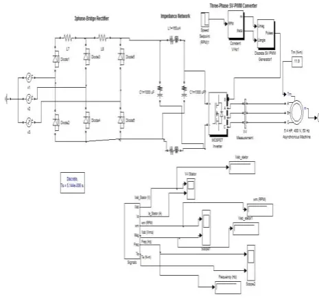
For the simulation of ZSI,we uses following parameters value as given below:
L1=L2=160µH.
C1=C2=1000µF.
AC source voltage =400 V,60 Hz AC supply Load : 3 phase,5.4HP, 440V,1430 rpm asynchronous machine.
[image:4.595.320.553.210.428.2]The simulation diagram of Z source inverter fed with AC load as shown in below fig.
Fig 6: Simulation diagram of ZSI fed with AC load
For the improvement in the performance of the AC load such induction motor we need to be considered some output parameter should not get adversely affected.Hence,some of the energy conversion application rectification from AC supply to DC supply by the inversion carried by inverter, where have greater chances of the
adverse effect on speed, line
voltage,statorvoltage,statorcurrent.Similarly,for such parameters we need to calculate precise and suitable values of impedance networkelements.For simulation of the proposed system, we usesnclosed loop induction motor drive with constant V/Hz method. This method helps to limit slip speed (being diferent between synchronous speed and electrical rotor speed),offset voltageand reference speed can be externally adjusted.This external adjustement allows tuning or matching of the induction motor drive to converter and or inverter and tailoring of its characteristics to match load requirement.
3. SIMULATION RESULTS:
© 2017, IRJET | Impact Factor value: 5.181 | ISO 9001:2008 Certified Journal | Page 364 Fig 7 :stator voltage and stator current without
proposed ZSI
[image:5.595.331.538.110.257.2]Fig 8: Angular speed (rpm) and line voltage without proposed ZSI
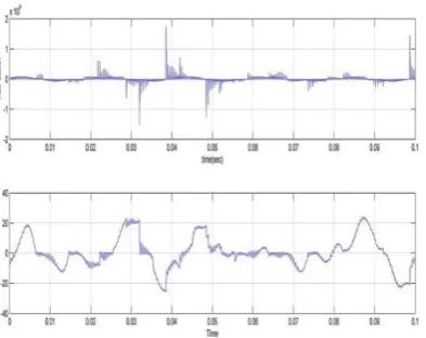
[image:5.595.332.540.310.451.2]Fig 9 :Frequency and torque without ZSI
Fig 10 :Stator voltage and stator current with proposed ZSI.
Fig 11 : Angular speed (rpm) and line voltage with proposed ZSI
.
Fig 9 : Frequency and torque without ZSI
[image:5.595.61.261.317.485.2] [image:5.595.328.541.500.640.2] [image:5.595.61.267.552.696.2]© 2017, IRJET | Impact Factor value: 5.181 | ISO 9001:2008 Certified Journal | Page 365 For VSI, due to speed variation,stator current exceeds
rated current by many times,thus endangering the inverter-converter combination.Due to symmetrical combination of capacitors and inductors stator current does not exceeds rated current therefore there is lowering possibilities of endangering the inverter-converter combination.
Torque is unable to behaves transiently due to the oscillations in the roto flux linkage,results in larger stator current and torque transients in the case of the VSI.Whereas in the case of ZSI torque behaves transiently when motor achives the synchronous speed.
Stator voltage waveform of the VSI rich in the harmonics.These time harmonics produces rotor current harmonics which turn interact with fundamental air gap flux,generating harmonics torque pulsation which are undesirable which may leads to audible noise and speed pulsation.These can be avoided in the ZSI.
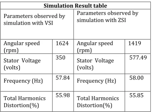
[image:6.595.30.286.413.601.2]According to the simulation results shown above the following parameters was observe numerically as shown in table-1
Table -1: Result Table
Simulation Result table Parameters observed by
simulation with VSI
Parameters observed by simulation with ZSI
Angular speed
(rpm) 1624 Angular speed (rpm) 1419 Stator Voltage
(volts)
350 Stator Voltage (volts)
577.49
Frequency (Hz) 57.84 Frequency (Hz) 58.00
Total Harmonics
Distortion(%) 55.98 Total Harmonics Distortion(%)
55.85
4. CONCLUSIONS
The simulation of z source inverter with traditional voltage source inverter are compared with different parameters.According to that, ZSI improves the performance of the induction motor drive with the help of implementation of the constant V/Hz control strategy for Z –source inverter fed induction motor in closed loop control.The barriers present in traditional inverter strategies can be overcome by using ZSI which are shown by the results.
REFERENCES
[1] F. Z. Peng, “Z-source inverter,” IEEE Trans. Ind. Applicat., vol. 39, no.2, pp. 504–510, Mar./Apr. 2003. [2] M. Shen, J.Wang, A. Joseph, F. Z. Peng, L. M. Tolbert,
and D. J. Adams, “Maximum constant boost control of the Z-source inverter,” presented at the IEEE Industry Applications Soc. Annu. Meeting, 2004.
[3] F. Z. Peng, M. Shen, and Z. Qian, “Maximum boost control of the z-source inverter,” in Proc. 39th IEEE Industry Applications Conf., vol. 1, Oct. 2004.
[4] Atul Kushwaha, Mohd. Arif Khan,Atif Iqbal, “Z- Source Inverter Simulation and Harmonic Study”, Global Journal of Advanced Engineering Technologies-Vol1-Issue1-2012 ISSN: 2277-6370.
[5] Miaosen Shen, Jin Wang,Alan Joseph, Fang Zheng Peng, Leon M. Tolbert,Donald J. Adams, “Constant Boost Control of the Z-Source Inverter to Minimize Current Ripple and Voltage Stress”,IEEE transactions on industry applications, vol. 42, no. 3, May/June 2006 [6] Yu Tang, Member, IEEE, Shaojun Xie, Member, IEEE,
and Chaohua Zhang, “Single-Phase Z-Source Inverter”,IEEE transactions on power electronics, vol. 26, no. 12, december 2011.
[7] Omar Ellabban, Joeri Van Mierlo, Philippe Lataire, “A Comparative Study of Different Control Techniques for an Induction Motor Fed by a Z Source Inverter for Electric Vehicles”,proceedings of the 2011 International Conference on Power Engineering, Energy and Electrical Drives, Torremolinos (Málaga), Spain. May 2011.
[8] Yam P. Siwakoti, Fang Zheng Peng,Frede Blaabjerg, Poh Chiang Loh,Graham E. Town, “Impedance-Source Networks for Electric Power Conversion Part I: A Topological Review”, IEEE Transactions On Power Electronics, Vol. 30, No. 2, February 2015