HIGH-PERFORMANCE SILICON NANOWIRE ELECTRONICS
Thesis by
Ruo-Gu Huang
In Partial Fulfillment of the Requirements for the
Degree of
Doctor of Philosophy
CALIFORNIA INSTITUTE OF TECHNOLOGY
Pasadena, California
2012
2012
Ruo-Gu Huang
ACKNOWLEDGEMENTS
It is indeed a wonderful journey to conduct my Ph.D. study at Caltech. First of all, I would
like to express my gratitude and thanks to my advisor, Professor Jim Heath, for his support
and guidance on my research over the past six years. Jim is an amazing person to work
with. His scientific insight always inspires me to think deeper. I really learn a lot from him.
I also want to thank my Defense and Candidacy Committee members: Professor
Amnon Yariv, Professor Alex Scherer, Professor Keith Schwab, Professor Julia Greer,
Professor Alain Martin, and Professor Azita Emami, for their insightful suggestions on my
thesis and presentation.
I am grateful to my intelligent colleagues in the Heath group. It is really a pleasure to
work with you. Special gratitude goes to some current and past group members. I want to
thank Dr. Douglas Tham, Professor Dunwei Wang, Dr. Bonnie Kean, Dr. Young-Shik Shin,
and Dr. Habib Ahmad, whom I worked with on the silicon nanowire logic project. In
addition, I also acknowledge Jen-Kan Yu, Dr. Ke Xu, Dr. Slobodan Mitrovic, and Joey
Varghese for their help on my current memory project. I am grateful to Kevin Kan for his
equipment support. My appreciation also goes to Diane Robinson and Amy Crown for their
administration assistance.
I want to thank Kent Potter in the EE Department for his instrument assistance. Also,
I thank Brian Thibeault at UCSB for his help on ALD process. I appreciate the help coming
from Jim Lacy, Melissa Melendes, Dr. Guy DeRose, and Nils Asplund, the staff members
My gratitude also goes to all of my friends at Caltech, especially those affiliated with
the Association of Caltech Taiwanese. Without you, my life would not be this colorful.
Last but not least, I want to express my deepest gratitude to my family, especially my
father, and my wife, for their endless love, support, and motivation. My father, the bravest
cancer fighter, leads by example, for which I am always indebted. I will keep his devotion
to my family in mind forever. Finally, I would like to thank my wife, Wan-Yu, for pushing
me through my Ph.D. study. I cannot imagine going through all of this alone without her
ABSTRACT
This thesis explores 10-nm wide Si nanowire (SiNW) field-effect transistors (FETs) for
logic applications via the fabrication and testing of SiNW-based ring oscillators. Both
SiNW surface treatments and dielectric annealing are reported for producing SiNW FETs
that exhibit high performance in terms of large on/off-state current ratio (~108), low drain-induced barrier lowering (~30 mV), high carrier mobilities (~269 cm2/V·s), and low subthreshold swing (~80 mV/dec). The performance of inverter and ring-oscillator circuits
fabricated from these nanowire FETs is explored as well. The inverter demonstrates the
highest voltage gain (~148) reported for a SiNW-based NOT gate, and the ring oscillator
exhibits near rail-to-rail oscillation centered at 13.4 MHz. The static and dynamic
characteristics of these NW devices indicate that these SiNW-based FET circuits are
excellent candidates for various high-performance nanoelectronic applications.
A set of novel charge-trap non-volatile memory devices based on high-performance
SiNW FETs are well investigated. These memory devices integrate Fe2O3 quantum dots
(FeO QDs) as charge storage elements. A template-assisted assembly technique is used to
align FeO QDs into a close-packed, ordered matrix within the trenches that separate highly
aligned SiNWs, and thus store injected charges. A Fowler-Nordheim tunneling mechanism
describes both the program and erase operations. The memory prototype demonstrates
promising characteristics in terms of large threshold voltage shift (~1.3 V) and long data
retention time (~3 × 10⁶ s), and also allows for key components to be systematically varied. For example, varying the size of the QDs indicates that larger diameter QDs exhibit a larger
transport. The device temperature characteristics reveal an optimal window for device
performance between 275K and 350K.
The flexibility of integrating the charge-trap memory devices with the SiNW logic
devices offers a low-cost embedded non-volatile memory solution. A building block for a
TABLE OF CONTENTS
Acknowledgements ... iv
Abstract ... vi
Table of Contents ... viii
List of Figures and Tables ... xi
Chapter 1: Introduction ... 1
1.1 Silicon Nanowire Electronics ... 1
1.2 Thesis Overview ... 4
Chapter 2: Enhanced-Mode Silicon Nanowire Field-Effect Transistors ... 5
2.1 Introduction ... 5
2.2 Pattern Doping Protocol ... 7
2.2.1 Spin-on-Doping Technique ... 8
2.2.2 Ion Implantation ... 9
2.3 Superlattice Nanowire Pattern Transfer (SNAP) ... 10
2.4 Surface Passivation Technique ... 12
2.5 Development of Complementary Silicon Nanowire Field-Effect Transistors ... 13
2.5.1 Device Fabrication ... 13
2.5.2 Device Electrical Characteristics ... 16
2.5.3 Parameter Fluctuations ... 20
2.6 Conclusions ... 22
Appendix 2.1: The Process Detail of HfO2 Thin Films Prepared by Using Atomic Layer Deposition (ALD) . ... 24
Appendix 2.2: Mobility Comparison SiNW FETs ... 25
Appendix 2.4: Estimate of the Reduction in the HfO2
Interface-Trap Density ... 27
Chapter 3: High-Performance Silicon Nanowire Logic Circuits ... 28
3.1 Introduction ... 28
3.2 Silicon Nanowire Inverters ... 29
3.2.1 Static Electrical Characteristics ... 30
3.2.2 Transient Electrical Characteristics ... 33
3.2.3 Inverter Parameter Fluctuations ... 34
3.3 Silicon Nanowire Ring Oscillators ... 35
3.3.1 HSPICE Simulation of Three-Stage Ring Oscillators ... 36
3.3.2 Transient Electrical Characteristics ... 37
3.3.3 Performance Analysis ... 38
3.2.4 Circuit Performance Fluctuations ... 39
3.4 Conclusions ... 40
Appendix 3.1: Performance Comparison of SiNW ROs ... 41
Chapter 4: Silicon Nanowire Non-volatile Memory Devices ... 42
4.1 Introduction ... 42
4.2 Development of Silicon-Nanowire Quantum-Dot Non-volatile Memory Devices ... 44
4.2.1 Device Fabrication ... 44
4.2.2 Device Electrical Characteristics ... 48
4.2.3 The Quantum Dot Size Dependence on Memory Window ... 53
4.2.4 Device Temperature Characteristics ... 54
4.3 Conclusions ... 56
Appendix 4.1: Template-Assisted Assembly Technique ... 57
Appendix 4.3: The Transfer Characteristics of n-Type
Memory Devices ... 59
Appendix 4.4: Calculation of the Capacitive Coupling Ratio of a Memory Device ... 60
Appendix 4.5: Calculation of the Average Number of Stored Charges per FeO QD ... 61
Chapter 5: Future Work ... 62
5.1 Ultra-dense SiNW Charge-Trap Memory ... 62
5.2 SiNW-Based Field-Programmable Gate Array (FPGA) ... 64
LIST OF FIGURES AND TABLES
Chapter 1
Figure 1.1 Potential technology solutions of future logic devices ... 2
Chapter 2 Figure 2.1 Simplified cross-sectional view of an n-type FET ... 6
Figure 2.2 Doping scheme of complementary SiNW FETs ... 8
Figure 2.3 Major steps of SNAP process ... 10
Figure 2.4 High-magnification SEM micrograph of SiNW array ... 11
Figure 2.5 SiNW-based FETs and circuits ... 14
Figure 2.6 SiNW FET performance measurements ... 16
Figure 2.7 Histogram of threshold voltages of SiNW FETs ... 20
Figure 2.8 Histograms of on/off-state current ratio of SiNW FETs ... 22
Figure 2.9 Histograms of transconductance of SiNW FETs ... 23
Table 2.1 Summary of key performance metrics of SiNW FETs ... 17
Table 2A.1 Comparison of mobility values of SiNW FETs ... 25
Table 2A.2 Comparison of subthreshold swing values of SiNW FETs ... 26
Chapter 3 Figure 3.1 Detail layout of SiNW circuit ... 29
Figure 3.2 Static characteristics of a SiNW inverter ... 31
Figure 3.3 Voltage gain of a SiNW inverter at different bias ... 32
Figure 3.4 Dynamic characteristics of a SiNW inverter ... 33
Figure 3.5 Statistic data of SiNW inverters ... 34
Figure 3.6 HSPICE simulation of three-stage ring oscillator ... 36
Figure 3.7 Oscillation waveform of a SiNW ring oscillator ... 38
Table 3A.1 Comparison of ring oscillator performance ... 41
Chapter 4 Figure 4.1 Schematic of SiNW charge-trap memory ... 45
Figure 4.2 Transfer characteristics of a memory device ... 48
Figure 4.3 Voltage and speed test of a memory devices ... 49
Figure 4.4 Endurance and retention test of a memory devices ... 50
Figure 4.5 Low-voltage endurance test of a memory device ... 51
Figure 4.6 QD size dependence on threshold voltage shift ... 53
Figure 4.7 Temperature characteristics of a memory device ... 55
Figure 4S.1 F-N plot of a memory device ... 58
Figure 4S.2 Transfer characteristics of n-type memory devices ... 59
Figure 4S.3 Simplified capacitor model of a memory device ... 60
Chapter 5 Figure 5.1 SEM micrograph of Si nanomesh and memory devices ... 63
Chapter 1
Introduction
1.1
Silicon Nanowire Electronics
Silicon nanowires (SiNWs) have received attention as biological [1] and chemical [2]
sensors, and as thermoelectric [3, 4], photovoltaic [5], and nanoelectronic devices [6, 7].
For virtually all of these applications, improvements in nanowire electronic properties for
both n- and p-type doping, as well as improvements in the ability to control those properties,
leads to superior performance. For applications such as thermoelectric energy conversion
[4], or biomolecular sensing, decreasing the nanowire diameter can potentially yield
performance increases, but only if the electronic properties of the nanowires can be well
controlled. In addition, many NW applications, including thermoelectrics, require both n-
and p-type NWs. Thus, techniques for producing and fine-tuning the properties of high
performance SiNWs are finding applications that go well beyond conventional electronics
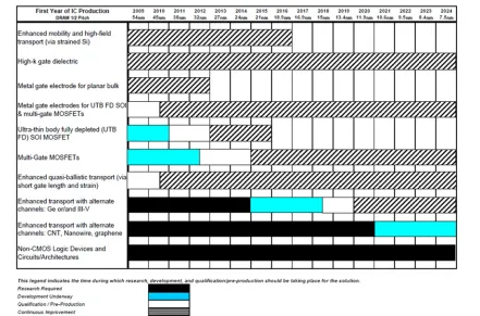
Figure 1.1 Potential technology solutions of future logic devices. These solutions are projected by International Technology Roadmap for Semiconductors (ITRS) in 2009.
SiNW field-effect transistors (FETs) provide the most important class of devices for
investigating and optimizing NW electronic properties, regardless of the final intended
application. Conventional planar bulk FETs suppress the short-channel effects (SCEs) and
adjust the threshold voltages via modulating the channel doping concentration. The demand
of high channel doping with scaling results in band-to-band tunneling across the junction,
gate-induced drain leakage, and mobility degradation [8]. Furthermore, the more and more
severe random dopant variation in scaled devices can cause intolerable threshold voltage
variation [8, 9]. Consequently, it is difficult to further compromise this approach as scaling
continues. Fully-depleted (FD) channel multi-gate FETs can solve this issue because they
can adjust the threshold voltages by engineering the work function of the gate materials
[image:14.612.106.547.381.672.2]these multi-gate devices can also have good SCE immunity [10-12]. Thus, FD multi-gate
architecture is well recognized as a solution to the technology nodes below 32 nm [6-8, 13],
as shown in Figure 1.1 [8]. Since the unique geometry of SiNWs can enable the
straightforward implementation of multi-gate, all the SiNW devices mentioned through this
thesis are built based on the FD multi-gate architecture.
SiNW-based devices can be fabricated from both bottom-up (materials grown)
NWs [14, 15] or top-down, lithographically patterned NWs [6, 16]. Our own SiNWs,
which are formed using the Superlattice Nanowire Pattern Transfer (SNAP) method [17,
18], are somewhere in between these two limits. The template used to pattern the SNAP
NW arrays is grown using materials approaches, but the NWs themselves are formed from
a (pre-doped) silicon-on-insulator thin films. The SNAP NWs possess both advantages and
disadvantages relevant to their top-down and bottom-up fabricated counterparts. For
example, the SNAP patterning approach allows for the formation of extremely long
(~2-mm) NW arrays at a NW width (≥7 nm) and pitch (≥13 nm) [17, 19] that are difficult to
achieve using any alternative approach. However, although SNAP NW arrays are relatively
straightforward to integrate into simple logic and memory circuits [18-20], arbitrarily
complex, wafer-scale NW circuits are not within reach—similar to the case for materials
grown SiNWs. Thus, in Chapter 2 and 3, we compare our results against devices reported
1.2
Thesis Overview
This thesis is organized into five chapters to accommodate my research projects in Heath
group at Caltech. Each chapter was organized to be largely self-contained. All chapters
share the same reference list at the end of this thesis. To avoid excessive redundancy,
similar process techniques that are required in later chapters were occasionally referenced
to an earlier chapter.
In Chapter 2, I first present the SNAP technique, which is used to fabricate
high-quality silicon nanowires as my research basis. Two Si doping techniques are reported to
make lightly-doped transistor channel regions and highly-doped source/drain contacts.
SiNW surface treatment and HfO2 gate dielectric annealing are described in detail to reach
low interface-trap density. The electrical characteristics of the SiNW-based FETs are well
explored and compared to the state-of-the-art performance metrics. In Chapter 3, the
fabrication and characterization of SiNW inverters and three-stage ring oscillators are
presented. Both static and dynamic circuit performance is found to be excellent.
Nevertheless, large statistic variation on some key parameters is observed for the devices
and circuits. Asynchronous circuit architecture is proposed to adapt to this inevitable
variability. In Chapter 4, I demonstrate a novel type of SiNW charge-trap memory device
that integrates iron oxide quantum dots as charge storage elements. This type of memory
device shows promising electrical characteristics and can be easily integrated with the
developed SiNW logic devices to offer a low-cost embedded memory solution. Based on
these fundamental works mentioned earlier, a SiNW-based FPGA platform is proposed in
Chapter 2
Enhanced-Mode Silicon Nanowire
Field-Effect Transistors
Partial results presented in this chapter are reproduced with permission
from Huang, R.-G., et al. “High performance ring oscillators from
10-nm wide silicon nanowire field-effect transistor,” Nano Research, vol. 4,
no. 10, pp. 1005-1012, 2011.
2.1
Introduction
Enhanced-mode field-effect transistors (FETs) are normally-off devices. Unlike a
normally-on FET (e.g., a depletion-mode FET), an enhanced-mode FET does not have a
conductive channel when applying zero gate voltage. The normally-off characteristic can
be explained as follows. Figure 2.1 shows the simplified physical structure of an
enhanced-mode FET. The device is fabricated on a lightly p-doped Si substrate. The heavily
n-doped source and drain regions are intentionally separated by the p-type substrate, where
the spacing is defined as transistor channel length. Each pair of n+ region and p- substrate can form a p-n junction diode. When no bias voltage applied to the gate, the two
back-to-back diodes prevent current conduction from drain to source. Such normally-off
characteristic makes enhanced-mode FETs very suitable for low standby power
Figure 2.1 Simplified cross-sectional view of an enhanced-mode n-type FET. The p-n junction between substrate and source/drain is modeled by a diode.
semiconductor industry. For convenience, FET is short for enhanced-mode FET through
this thesis unless specified otherwise.
In this chapter, we explore 10-nm wide Si nanowire (SiNW) FETs for logic
applications. Here highly-ordered SiNWs are the main building block to serve as transistor
channel regions. The fully-depleted multi-gate architecture discussed in Chapter 1 is
implemented on our SiNW FETs. We report on Si doping protocols, SiNW patterning
technique, SiNW surface treatments, and gate dielectric annealing, for producing SiNW
FETs that exhibit high performance in terms of large on/off-state current ratio (~108), low drain-induced barrier lowering (~30 mV) and low subthreshold swing (~80 mV/dec). In
addition, we report on the effective electron and hole mobilities, which we find to be at the
2.2
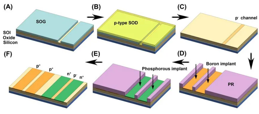
Pattern Doping Protocol
Our SiNW FETs were fabricated on 6” (100) SIMOX SOI wafers with nominally
30-nm-thick single crystal silicon (100) film on top of 250 nm SiO2 (Simgui, Shanghai, China). Since our pattern doping procedures were not self-aligned, the Moiré techniques [21] were
adopted to achieve ~0.1 μm alignment accuracy. To avoid the possible metal diffusion in
the following thermal process, silicon was chosen as the alignment mark material. The
50-nm-thick silicon alignment marks were first formed on the starting SOI wafer via the
e-beam evaporation and standard lift-off process. The fabrication of complementary FETs
requires three pattern doping processes. In order to match the device threshold voltages, the
p-type spin-on-dopant (SOD) was used to increase the n-FETs’ channel doping
concentration whereas the p-FETs’ channel regions are intentionally left undoped. Then
two separate ion implantations were sequentially carried out to define the heavily-doped
source/drain regions of n- and p-FETs. Figure 2.2 summaries the key steps of the doping
Figure 2.2 The doping scheme of complementary SiNW FETs. The spin-on-doping technique was used to lightly dope the channel regions of n-FETs. Two separate ion implantations were sequentially carried out to heavily dope the source/drain regions of both types of FETs.
2.2.1
Spin-on-Doping Technique
The p-type spin-on dopant was used to dope n-FETs’ channel regions. This relatively
gentle doping technique prevents the formation of lattice defects that can be generated
using ion implantation [22]. The SOI wafers were first cleaned in dark using modified RCA
process (H2SO4:H2O2 = 3:1 v/v, 120 °C, 10 min; HF:H2O = 1:100 v/v, 15 s; HCl:H2O2:H2O = 1:1:6 v/v, 75 °C, 10 min). This clean recipe was modified to reduce the Si consumption during the cleaning. A 180-nm-thick spin-on-glass (SOG) (Accuglass 214, Honeywell,
Chandler, AZ) was then spin-coated (8000 RPM, 30 s) on the wafers as a dopant diffusion
barrier layer. The diffusion window was open via photolithography and wet etching (100%
BOE, 30s), as shown in Figure 2.2A. The modified RCA process was carried out again to
clean the exposed silicon. A p-type SOD film (Boron A, Filmtronics Inc., Butler, PA) was
a rapid thermal processor. The thermal drive-in process made dopants only diffuse into
silicon through the pre-defined window where the SOD film directly contacted with silicon.
The stacked SOG and SOD films were removed by BOE etching until the surface turned
hydrophobic (Figure 2.2C). The doping concentration was measured ~1017 cm-3 via four-point probe technique on a blank monitor wafer.
2.2.2
Ion Implantation
The p-type implantation (boron dose of 3.8 × 1014 cm-2 at 5 keV, Core Systems, Sunnyvale, CA) was first conducted to heavily dope the source/drain regions of p-FETs. The implanted
regions were defined by using photolithography (Figure 2.2D). The same protocol was
repeated for n-type implantation (phosphorus dose of 3.2 × 1014 cm-2 at 10 keV), as shown in Figure 2.2E. To prevent inconsistent implantation profiles caused by channeling, the
implanted wafers were tilted by 7˚ relative to the incident beam direction [23].
After the modified RCA cleaning, the implant thermal activation step was
performed under N2 at 900 °C for 10 s. The four-point probe technique was used to monitor the doping concentration. The concentration values of the heavily n- and p-doped Si are 2.4
× 1019 and 1.9 × 1019 cm-3, respectively. The same technique was also used to investigate the resistivity of 10-nm SiNWs that were made of implanted Si thin film. The result shows
that the SiNW resistivity (2.57 mΩ-cm) is comparable to the value of the implanted thin
film (2.15 mΩ-cm). This finding implies our thermal activation step can effectively anneal
doping profile is shown in Figure 2.2F, where the 1-μm channel length is defined by the
spacing of the adjacent source/drain regions.
2.3
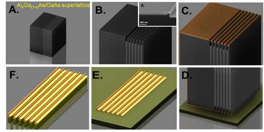
Superlattice Nanowire Pattern Transfer (SNAP)
The detail of SNAP process has been reported elsewhere [17, 18, 24, 25], and only the
most noticeable points are described here. Figure 2.3 shows the major steps in SNAP
nanowire fabrication. The superlattice wafer consisting of 100 alternating layers of GaAs
and AlxGa(1-x)As was created by metal-organic chemical vapour deposition (MOCVD)
[image:22.612.109.532.377.589.2](IQE Ltd., Cardiff, UK). Both composition and thickness can be well controlled in atomic
resolution. The thickness of each layer of GaAs and AlxGa(1-x)As is 60- and 10-nm, respectively. The SNAP process begins by cleaving a small piece (~2-mm wide and 5-mm
long) of superlattice that was served as a template for nanowire patterning (Figure 2.3A).
The cleaved template was gently cleaned in methanol to make sure there are no visible
particles on the surface. The template was then selectively etched (NH3: H2O2: H2O =
1:20:300 v/v, 10s; H2O2, 5s; H2O, 20s, all are at room temperature) to remove partial GaAs on the surface, leaving a comb of ~50-nm-high parallel AlxGa(1-x)As ridges (Figure 2.3B).
A thin layer (~100 Å) of Pt was evaporated on the template to create Pt nanowires along
the AlxGa(1-x)As ridges (Figure 2.3C). The Pt nanowires were brought into contact with the
Si wafer coated (6000 RPM, 30 s) with a thin layer of heat-curable epoxy (20 drops part A
to 2 drops part B (Epoxy Bond 110, Allied High Tech Products, Ranch Dominguez, CA)
plus 0.25 mL poly(methyl methacrylate) in 15 mL chlorobenzene), as shown in Figure
2.3D. To ensure the epoxy coating is uniform, the Si wafer should be thoroughly cleaned
beforehand. After epoxy curing, the entire assembly was immersed in the etchant (H2O2:
H3PO4: H2O = 1:5:50 v/v, ~6-7 hr). The
template was slowly dissolved to release
the Pt nanowires to the Si wafer (Figure
2.3E). The Pt nanowires served as an
etch mask for directional reactive ion
etching (RIE) (CF4 to He = 20:30, 5
[image:23.612.116.334.519.645.2]mTorr, 40 W, 4 min) to convert the
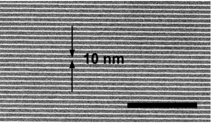
Figure 2.4 A high-magnification SEM
underlying 30-nm thin Si film into a Si nanowire array (Figure 2.3F). In our FET
fabrication, we routinely used SNAP technique to produce high-quality SiNW arrays
(Figure 2.4).
2.4
Surface Passivation Technique
The native oxide on the SiNW surface can carry a high density of positive charges [26],
which can reduce many FET performance metrics, including even inverting n-FETs in the
absence of an applied gate bias [20]. In addition, growing a high-quality, thin silicon
dioxide on SiNW surface is also a key process step for integrating a high-κ hafnium oxide,
which is used as FET gate dielectrics [27-29]. Thus, prior to FET metallization, the SiNW
arrays were passivated with a ~4-nm thermal oxide [30]. The SiNWs first went through the
modified RCA clean and then annealed under O2 in a RTP (1000 °C, 15 s, ramp rate: 35
°C/s) followed by a forming gas (5% H2 in N2, 475 °C, 5 min) anneal. This surface treatment, which significantly improved all FET performance metrics, is similar to what
2.5
Development of Complementary Silicon Nanowire
Field-Effect Transistors
2.5.1
Device Fabrication
The details of some key process steps have been covered in previous sections. Here they
are integrated to fabricate SiNW FETs. A 1-μm effective channel length was used in the
SiNW FETs and circuits (Chapter 3) for concept demonstration. Shorter channel lengths
Figure 2.5 SiNW-based FETs and circuits. (A) SiNW inverter fabrication scheme. (A1) SNAP Pt NWs are released onto the SOI substrate. (A2) Additional Pt masking stripes are patterned over the Pt NWs. The mask pattern is transferred into the underlying Si with RIE. (A3) The transferred and sectioned structure consists of lightly-doped single-crystalline SiNWs contacted to highly-doped Si pads. (A4) SiNW inverter is formed after gate dielectric deposition, metallization and metal gate definition. (b) SEM image of two 3-stage ROs and one inverter. Scale bar, 50 μm.
The SiNW FETs (Figure 2.5A) were fabricated on the pre-doped SOI wafers. The
SNAP method was utilized to prepare arrays of 2-mm-long, 10-nm-wide SiNWs. The
SNAP method initially produced an etch mask of Pt NWs on an epoxy-coated SOI surface
(Figure 2.5A1). Prior to translating the Pt NW pattern to the underlying SOI,
photolithography and lift-off processes were used to define contact pads within the NW
array (Figure 2.5A2) [32]. The NW/micropatterned mask was transferred into the
underlying SOI with a directional RIE. After metal removal and sectioning (via
lithographic patterning and a dry etch: SF6:He = 5:15, 15 mTorr, 40W, 1 min 15 s), SiNW
were produced (Figure 2.5A3) [32]. Ohmic metal electrode contacts were made to the Si
pads (Figure 2.5A4). High-quality SiNW arrays were routinely produced with this
technique.
A relatively large pitch (for SNAP) is required for the construction of multi-gate
structures in which the top and sidewalls of the NW channels are gated. Thus, we prepared
70-nm pitch SNAP NW arrays, which were then coated conformally with a ~6-nm thick
hafnium oxide (HfO2) gate dielectric at 250 °C using atomic layer deposition (see Appendix 2.1 for ALD process detail). This condition for depositing the HfO2 dielectric is
not ideal, but it also does not limit our final circuit performance. Pt and Ti gate electrodes
were used for the n- and p-FETs, respectively, to match FET threshold voltages. Figure
Figure 2.6 SiNW FET performance measurements. (A) Transfer characteristics of n- and p-FETs. Both the n- and p-FETs show very little hysteresis, which is negligible in the following parameter extraction. (B) Transfer characteristics of n- and p-FETs fabricated with the additional HfO2 anneal step. (C) Output characteristics of the devices shown in (A).
2.5.2
Device Electrical
Characteristics
Figure 2.6A shows the transfer
characteristics of the n- and p-FETs
consisting of twenty 10-nm SiNWs with
1-μm channel length (Lg). Both n- and p-FETs show very little hysteresis,
which is neglected in the following
parameter extraction. A full list of the n-
and p-FET performance numbers are
presented in Table 2.1. Here we simply
touch on a few key highlights. The
extracted threshold voltage (VTH) values
with |VDS| = 100 mV for the n- and p-FETs are ~1.98 and –1.17 V,
respectively, which confirm that both
devices are enhancement-mode FETs.
We have recently found that the thermal
oxide passivation described above
be fabricated without the use of channel doping, although the channels were doped in this
work. In any case, only slight drain-induced barrier lowering (DIBL) was found, with
values ~37 and ~30 mV/V for the n- and p-FET, respectively. For |VDS| = 1 V, the values of
ION / IOFF were ~4.9 × 10⁶ and ~1.1 × 10⁸ for the n- and p-FETs, respectively. The high on/off-state current ratio comes from the low off-state current, which can be attributed to
the well-passivated SiNW surface [26]. A high-quality (thermal) silicon dioxide passivation,
followed by hydrogen passivation, can dramatically reduce the surface state density of Si
[image:29.612.103.546.374.500.2]NWs [26, 30] and leads to superior gating efficiency.
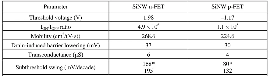
Table 2.1 Summary of key performance metrics of the SiNW n-and p-FETs discussed in the main text
Parameter SiNW n-FET SiNW p-FET
Threshold voltage (V) 1.98 –1.17 ION/IOFF ratio 4.9 × 10⁶ 1.1 × 10⁸ Mobility (cm2/(V·s)) 268.6 224.6 Drain-induced barrier lowering (mV) 37 30
Transconductance (μS) 6 4
Subthreshold swing (mV/decade) 168* 195
80*
132 * Improved subthreshold swing after dielectric forming gas annealing
The effective electron and hole mobilities, extracted in the linear operation region
[33], are ~268.6 and ~224.6 cm2/V·s, respectively. Both types of devices exhibit good mobility performance. These two comparable mobility values arise because the n-FET has
~100-fold higher concentration of channel dopants than does the p-FET. Table 2A.1 in
Appendix 2.2 compares the mobility values reported here with literature values for other
are only compared against other reported SiNW FETs using high-κ gate dielectrics.
Rudenko et al. [27] reported the state-of-the-art mobilities (260 and 175 cm2/(V·s) for electrons and holes, respectively) for top-down SiNW FETs with 2700 nm2 cross-section, which is almost 10 times greater than the SiNWs explored here. van Dal et al. [28] reported
electron and hole mobilities of 225 cm2/(V·s) and 175 cm2/(V·s) for 975 nm2 cross-section SiNW FETs. For bottom-up grown, 314 nm2 cross-section SiNW FETs, Zheng et al. [34] and Duan et al. [35] reported mobility values of 270 and 119 cm2/(V·s) for n- and p-FETs, respectively. Based upon the combined metrics of NW cross-section and carrier mobilities,
our SiNW FETs exhibit state-of-the-art performance, indicating that our SiNW surface
treatment effectively reduces surface scattering to maintain high mobilities [36].
The subthreshold swing (SS) parameter describes the effectiveness of an applied
gate voltage for switching a device between the on and off states; a smaller SS is preferred,
and implies a sharp transition between the on and off states of the FET. The SS of the
SiNW n- and p-FETs was initially measured as ~195 and ~132 mV/decade, respectively.
These values are not state-of-the-art, and are likely to be detrimentally influenced by the
high interface-trap density (Dit) [37] of the HfO2 dielectric at low deposition temperature
[38]. We hypothesize that an improved quality HfO2 film will boost this metric [39, 40]. We thus explored thermal annealing of the dielectric film, which has been previously
shown to reduce the Dit of HfO2 films [29, 40]. To prevent metal interconnects from reacting with silicon, the metallization was carried out after the deposited HfO2 film was
~169 and ~80 mV/decade, respectively. Such an improvement in SS values confirms our
hypothesis. The corresponding reduction in Dit of n- and p-FETs is estimated to be 1.7 and 3.4 × 1012 cm–2, respectively (see the Calculation in Appendix 2.3 for details). Table 2A.2 in Appendix 2.4 provides a comparison of SS values between our SiNW FETs and others
reported from the literature. Rudenko et al. [27] reported a SS of 61 mV/decade for
top-down fabricated, 2700 nm2 cross-section SiNW FETs. Higher SS values of 70 mV/decade have been reported by van Dal et al. [28] for top-down 780 nm2 cross-section SiNW FETs. For bottom-up n- and p-FETs (314 nm2 cross-section), the SS values of 300 and 62 mV/decade have been reported by Zheng et al. [34] and Richter et al. [29], respectively. A
high-quality, thin silicon dioxide on SiNW surface is a key process step for integrating
high-κ gate dielectrics that can yield a small SS [27-29]. While our SS values are good,
there is still significant room for improvement, again likely through improving the HfO2 quality by via a higher temperature deposition [38] and a higher temperature forming gas
anneal [40]. Nevertheless, the enhancement-mode n- and p-FETs without this second HfO2 anneal were sufficiently well matched to permit the fabrication of high quality inverters and,
via integration of three of those inverters, ring oscillator circuits. Figure 2.6C shows the
output characteristics of the n- and p-FETs used for the ROs. Both devices show high
output impedance in the pinch-off region, a characteristic that favors the inverter voltage
gain (Figure 3.2 inset). The output current of n- and p-FETs can be further matched by
properly sizing the sectioning mask of the complementary devices to accommodate
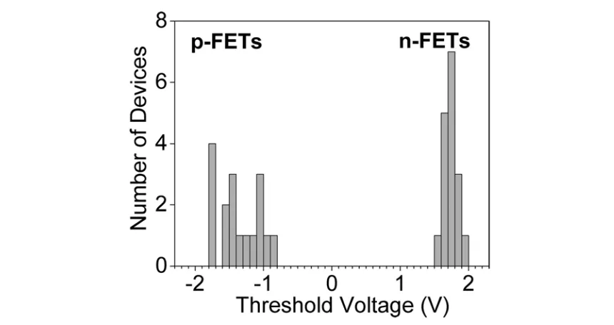
Figure 2.7Histogram of threshold voltages of SiNW n- and p-FETs.
2.5.3
Parameter Fluctuations
The SiNW circuit performance is mainly determined by some key FET parameters, such as
threshold voltage, on/off-state current ratio, transconductance, subthreshold swing, and
mobility. It is necessary to understand these parameter distributions to further optimize the
circuit performance. Among all of them, the threshold voltage distribution is the most
important one because it determines the circuit bias point and the applicable power supply
range. Figure 2.7 shows the histogram of threshold voltages of SiNW n- and p-FETs. Both
types of devices have 17 sample points. The mean value and the standard deviation of
n-FETs (p-n-FETs) are 1.762 (-1.354) and 0.104 (0.331), respectively. The relatively large
standard deviation for both types of devices is possibly attributed to the narrow width of
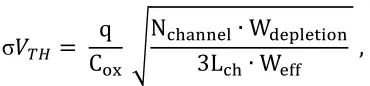
σ𝑉𝑇𝐻 = Cq ox �
Nchannel∙ Wdepletion
3Lch∙ Weff , (2.1)
where q is the electron charge, Cox is the gate oxide capacitance per unit area, Nchannel is the channel doping concentration, Wdepletion is the channel depletion width, Lch is the effective
channel length and Weff is the collective SiNW width. Since each SiNW in the FET devices is only ~10-nm in width, as equation (2.1) implies, any small width fluctuation or edge
roughness can contribute considerable threshold voltage variation [28].
The reason why p-FETs show larger variations is attributable to their lightly doped
channel. The channel has a low doping concentration of ~1015 cm-3, which is determined by the background doping of the starting SOI wafers. The calculation based on the device
parameters indicates there are only six dopant atoms in the p-FET channel regions. The
number and spatial distribution of dopant atoms can scatter around the average [41],
making the p-FET threshold voltage more vulnerable to doping fluctuation. This threshold
voltage variation caused by random-dopant fluctuation tends to increase with device
scaling [41-43]. A proposed approach that uses a ultra-thin (~20 nm) intrinsic SOI [28, 41,
43-45], and high-κ/metal three-dimensional gate stack [8, 10-12] can eliminate the need for
channel doping. The device threshold voltages can be adjusted by engineering the work
function of the gate materials without channel doping. Meanwhile the short-channel effects
[image:33.612.209.394.85.128.2]can be effectively suppressed by the excellent multi-gate controlled electrostatics.
Figure 2.8 shows the histogram of on/off-state current ratios of SiNW n- and
Figure 2.8 Histograms of on/off-state current ratio of SiNW n-FETs (A) and p-FETs (B). The data presented here are the identical devices used in Figure 2.7.
ratio. This is an important metrics for low power applications, in which a characteristic of
high on-state drive current but low off-state leakage is needed. The on-off ratio for the
majority of n-FETS (p-PETs) lies between 105 and 106 (107 and 108).Figure 2.9 shows the histogram of FET transconductance. Both types of devices show reasonable
transconductance distribution. High transconductance accompanied with high output
impedance (as show in Figure 2.6C) favors inverter voltage gain. The detail is discussed in
Section 3.2.1.
2.6
Conclusions
We have described the preparation of high performance SiNW n- and p-FETs, starting
from 10 nm × 30 nm cross-section SiNWs. The performance metrics of these devices are
compared against literature reports for FETs fabricated from both top-down and bottom-up
SiNWs. State-of-the-art performance metrics are observed for the individual SiNW FETs.
Figure 2.9 Histograms of transconductance of SiNW n-FETs (A) and p-FETs (B). The data presented here are the identical devices used in Figure 2.7.
performance. The nanofabrication approaches delineated here should find relevance in
Appendix 2.1 The Process Detail of HfO
2Thin Films Prepared by Using
Atomic Layer Deposition (ALD)
The conformal HfO2 thin films were prepared via a thermal ALD system (Savannah 100, Cambridge Nanotech Inc., MA) as FET gate dielectric. Tetrakis(dimethylamino)hafnium
(TDMAH) and water were used as the precursors. The deposition was conducted at 250 °C with a base pressure of ~0.3 torr. Each deposition cycle consists of the following four
characteristic steps:
Step 1 Exposure of TDMAH. A 0.2-s precursor pulse, followed by 5 s exposure.
Step 2 Purge of residual TDMAH. Pumping for 10 s.
Step 3 Exposure of water vapor. A 0.2-s water pulse, followed by 5 s exposure.
Step 4 Purge of residual water. Pumping for 10 s.
The film thickness was characterized by an ellipsometer (Sopra GES-5, SopraLab,
France) on blank Si wafers. The characterized deposition rate is ~1 Å/cycle. An array of
metal-insulator-metal capacitors was fabricated to extract the film dielectric constant. The
extracted dielectric constant is ~15.9.
The ALD HfO2 thin films were difficult to remove via a dry etching. In the device fabrication, a 1% hydrofluoric acid was used to etch HfO2. The etching rate strongly depends on the ALD temperature and the follow-up annealing conditions. For the as-made
Appendix 2.2 Mobility Comparison of SiNW FETs
Table 2A.1 Comparison of the SiNW n-and p-FET mobility values reported here with literature values for other SiNW FETs
Reference
SiNW dimensions/ Cross-section area/ NW preparation approach
Channel
length Gate dielectric
Electron mobility (cm2/V·s)
Hole mobility (cm2/V·s)
This work WSiNW = 10 nm; TSiNW = 30 nm /
300 nm2 / Top-down 1 μm
4 nm SiO2 +
6 nm HfO2
269 225
Suk,
IEDM ’07 [46]
4.5 nm in diameter /
15.9 nm2 / Top-down NA 3 nm SiO2 ~150 ~290
Tezuka,
IEDM ’07 [47]
WSiNW = 18 nm; TSiNW = 38 nm /
684 nm2 / Top-down 20 μm 15~18 nm SiO2 ~200 ~140
van Dal,
VLSI ’07 [28]
WSiNW = 15 nm; TSiNW = 65 nm /
975 nm2 / Top-down 0.9 μm
1 nm SiO2 +
2.5 nm Hf0.4Si0.6O2
~225 ~175
Gunawan,
Nano Lett. ’08 [48]
WSiNW = 20 nm; TSiNW = 20 nm /
400 nm2 / Top-down 0.5 μm 5 nm SiO2 ~370 ~130
Chen,
JJAP ’09 [49]
WSiNW = 48 nm; TSiNW = 22 nm /
1056 nm2 / Top-down 4 μm 13.6 nm SiO2 540 NA
Hashemi,
IEDM ’08 [50]
WSiNW = 44 nm; TSiNW = 8.7 nm /
382.8 nm2 / Top-down NA SiO2 ~325 NA
Rudenko,
Microelec. Eng. ’05 [27]
WSiNW = 45 nm; TSiNW = 60 nm /
2700 nm2 / Top-down 5 μm HfO2 ~260 ~175
Zheng,
Adv. Mater. ’04 [34]
20 nm in diameter /
314 nm2 / Bottom-up 2 μm 60 nm ZrO2 270 NA
Duan,
Nature ’03 [35]
20 nm in diameter /
Appendix 2.3 Subthreshold Swing Comparison of SiNW FETs
Table 2A.2 Comparison of the SiNW n-and p-FET subthreshold swing values reported here with literature values for other SiNW FETs using high-κ gate dielectrics
Reference
SiNW dimensions/ Cross-section area/ NW preparation approach
Channel
length Gate dielectric
SSn (mV/decade)
SSp (mV/decade)
This Work
WSiNW = 10 nm;
TSiNW = 30 nm / 300 nm2 /
Top-down
1 μm 4 nm SiO2 +
6 nm HfO2
169 80
Richter,
TED ’08 [29]
20 nm in diameter /
314 nm2 / Bottom-up 6 μm
3.5 nm SiO2 +
HfO2
NA 62
van Dal,
VLSI ’07 [28]
WSiNW = 12 nm;
TSiNW = 65 nm / 780 nm2 /
Top-down
80 nm 1 nm SiO2 +
2.5 nm Hf0.4Si0.6O2
~70 ~70
Rudenko,
Microelec. Eng. ’05 [27]
WSiNW = 45 nm;
TSiNW = 60 nm / 2700 nm2 /
Top-down
5 μm SiO2 + HfO2 ~61 ~61
Hu,
Nano Lett. ’08 [51]
15 nm in diameter /
177 nm2 / Bottom-up 100 nm 4 nm HfO2 NA 140
Zheng,
Adv. Mater. ’04 [34]
20 nm in diameter /
314 nm2 / Bottom-up 2 μm 60 nm ZrO2 300 NA
Duan,
Nature ’03 [35]
20 nm in diameter /
Appendix 2.4 Estimate of the Reduction in HfO
2Interface-Trap Density
Calculationapproach for estimating the reduction in the HfO2interface-trap density, based upon measured device characteristics with and without HfO2 dielectric annealing.
The subthreshold swing of FETs is given by [37]
, ) 1 ( 10 ln i it D C qD C q kT
SS ≈ ⋅ + +
where CD is the depletion-layer capacitance, Ci is the dielectric capacitance, and Dit is the
interface-trap density. We can rewrite the equation to express Dit as
(
)
.1 10
ln i D
i
it C C
q kT
SS C
D − ⋅ +
⋅ ⋅ ≈
We can estimate the Dit change if two devices have the same Ci and CD.
(
1 2)
.2 1
10
ln SS SS
kT C D D D i it it
it = − ≈ ⋅ −
δ
Chapter 3
High-Performance Silicon Nanowire
Logic Circuits
Partial results presented in this chapter are reproduced with permission
from Huang, R.-G., et al. “High performance ring oscillators from
10-nm wide silicon nanowire field-effect transistor,” Nano Research, vol. 4,
no. 10, pp. 1005-1012, 2011.
3.1
Introduction
In this chapter, both inverter and ring oscillator circuits (ROs) are explored as a driver to
develop SiNW FET arrays. Figure 3.1 shows the layout detail of current design. These
circuits require the integration of both n- and p-FETs and have strict, high-performance
requirements with respect to both types of devices. For example, the performance of a RO
is so sensitive towards many important NW metrics, nanowire- or nanotube-based ROs
have been widely investigated [6, 14-16, 52, 53]. In general, these published devices
exhibit oscillation frequencies in the megahertz to >100 MHz range, but other circuit
characteristics, such as output swing (which is the oscillation voltage amplitude) have been
poor. For example, if the output swing is divided by the magnitude of the supply voltage,
the largest ratio reported for a high-speed NW RO is only ~0.33 [6, 15]. Ideally, this ratio
Figure 3.1 The layout detail of SiNW inverters and ROs. In this design, each SNAP imprint has 10 circuit sections. There are one inverter and two ROs in each section. The probing pads attached to the ROs permit the direct access to their transient characteristics. This design is implemented via high throughput photolithography. The minimum circuit feature and the parasitic capacitance can be further scaled by engaging high-resolution e-beam lithography. Inset is the schematic of a three-stage RO. Scale bar in the SEM micrograph, 200 µm.
here that SiNW RO circuits, comprised of 10-nm wide, 30-nm high SiNWs can both
perform at >10 MHz while retaining an output swing/supply voltage ratio of 0.86.
3.2
Silicon Nanowire Inverters
A CMOS inverter is the most fundamental building block of modem digital circuits. A
CMOS inverter is composed of two matched n- and p-FET, which are connected in series.
In terms of power consumption, a CMOS inverter consumes only high dynamic power but
keep very low static power [54]. Such a power-efficient characteristic makes CMOS-based
developed in Chapter 2 were used to fabricate high-performance SiNW inverters. Both
inverter static and dynamic characteristics are investigated.
3.2.1
Static Electrical Characteristics
Figure 3.2 shows the static transfer characteristics of a SiNW inverter. It is reasonable to
bias the inverter with 1-μm channel length at 3 V. The operating voltage can be further
scaled down with device channel length and threshold voltage. The inverter noise margins
(NMs) are an important metrics that quantifies the ability of a NOT gate to reject the noise
superimposed on the input signal [54]. The high and low NM can be defined by the four
parameters obtained from the voltage transfer characteristic as follows.
NMH = VOH− VIH, (3.1)
Figure 3.2 Static characteristics of a SiNW inverter under 3-V bias. The black and green curves correspond to the voltage and current transfer characteristics, respectively. The inset shows the corresponding voltage gain.
where VOH, VIH, VIL, and VOL are the points at which the slope of the transfer characteristics is -1, as indicated in Figure 3.2. From the given transfer characteristics, the
inverter exhibits excellent noise margins: NML and NMH are 1.74 and 0.82 V, respectively.
In addition, the transfer characteristics also exhibit matched input/output range that permits
signal propagation without amplitude degradation. The value of inverter dc voltage gain is
a good index to evaluate the extent of signal propagation within logic gates. High voltage
gain is preferred. For VDD = 3 V, the maximum gain is ~148 (Figure 3.2 inset). To our
Figure 3.3 The voltage gain of a SiNW inverter at different bias combinations. The back-gate bias of 0, 5, 7.5, and 10 V are used to optimize the voltage gain.
voltage gain mainly arises from
the high FET transconductance
and large output impedance
described in Chapter 2. The
current transfer characteristics
shown in the same figure
indicate the inverter only
consume a considerable current
in the transition region, but
otherwise the quiescent current
stays low (at VIN = 0 volts,
IINVERTER ~13 pA). This excellent inverter quiescent behavior is attributed both to the low subthreshold current and to the high on/off current ratio of the FETs, which makes our
SiNW circuits suitable for low-power application.
Figure 3.3 further shows the inverter voltage gain dependence on different bias
conditions. As predicted, the voltage gain decreases with decreasing supply voltage that
causes smaller FET transconductance. Nevertheless, at a low supply voltage of 1.5 V, the
inverter still has voltage gain up to 13. In addition, the voltage gain can also be modulated
by the bias applied to the wafer backside. It is because the back-gate bias can introduce a
second channel at the bottom interface of SiNWs to modulate the total transconductance
contributed by n- and p-FET. Although the back-gate modulation is not as strong as its
top-gate counterpart due to the thicker equivalent top-gate dielectrics, it still offers another freedom
Figure 3.4 The dynamic characteristics of a SiNW inverter under V bias. The 4-MHz input signal was fed by a function generator. To buffer the circuit from the measurement setup, the measurement was done by the high-impedance active probe.
3.2.2
Transient Electrical Characteristics
Figure 3.4 shows the dynamic characteristics of the inverter, characterized by using an
active probe (Picoprobe 12C, GGB Industries, Inc., FL, USA). The low capacitance
loading of an active probe permits a high-fidelity transient measurement without changing
the circuit speed. The 10:1 signal attenuation intrinsic to the probe and the delay associated
with coaxial cables are compensated for in the data presented. The inverter can invert a
4-MHz sinusoidal input and maintain reasonable output swing. The swing amplitude
increases with decreasing input speed. A visible propagation delay (~85 ns) is observed.
Most of the delay arises from parasitic capacitances that are associated with the probe pad
and the circuit interconnects as shown in Figure 3.1. The internal gate delay, as addressed
Figure 3.5 Histogram of switching point (A) and voltage gain (B) of 16 SiNW inverters.
3.2.3
Inverter Parameter Fluctuations
Figure 3.5 shows the performance fluctuations of 16 SiNW inverters under 3-V bias. The
histogram of inverter switching points (SP) is shown in Figure 3.5A. The SP value is
defined as when the inverter input voltage is equal to the output voltage. We can use the SP
histogram to study the transition variation of SiNW inverters. The SP men value and the
standard deviation are 1.766 and 0.237, respectively. As discussed in Section 2.5.3, the SP
variation mainly arises from the threshold voltage fluctuation of SiNW FETs. Tighter SP
distribution can be achieved if the FET threshold voltages are better controlled. Figure 3.5B
shows the voltage gain histogram of SiNW inverters. Although most inverters have high
gain (>40), the relatively broad distribution may hinder these SiNW inverters from being
used in more complicated synchronous circuits. Nevertheless, asynchronous circuit
architecture offers an alternative approach [56, 57] for high-variability SiNW circuit. Since
robust to physical parameter variations. For example, an asynchronous circuit can tolerate
large variation of ambient temperature and the supply voltage while maintaining the correct
operation. More detail of asynchronous circuits is available in the following section.
3.3
Silicon Nanowire Ring Oscillators
Synchronous logic circuits feature a global clock that synchronizes circuit activity, and are
the standard of digital circuits. To avoid timing error, the clock speed of synchronous
circuits is determined by the worst-case delay of the longest signal path. However,
nanoscale circuits can exhibit stochastic variations in doping, device dimensions, and other
factors that can detrimentally influence the worst-case delay, which can make synchronous
logic circuits inefficient [56, 57]. Alternatively, asynchronous circuits have no global clock
but instead are comprised of computational modules communicating by handshake
protocols [56, 58] for local synchronization. Asynchronous systems have also demonstrated
to be energy and power efficient due to the absence of a global clock, the locality of
activity, and the automatic shut-off inactive parts. Oscillating handshake signals are
essential to keep an asynchronous circuit active. A key component of asynchronous logic
circuits is ring oscillators (ROs), which are comprised of odd number of inverters, and
provide for the local clocks that time such circuits. For ROs to maintain oscillation, large
gain and full signal-restoration are required. Thus, we report on SiNW-based ROs as a step
Figure 3.6 The HSPICE simulated output waveforms of three ring oscillators with different inverter gain. The voltage gains (from top to bottom) are 25, 10, and 5, respectively.
3.3.1
HSPICE Simulation of Three-Stage Ring Oscillators (RO)
Before fabricating SiNW ROs, the voltage gain dependence of three-stage ROs is first
investigated by conducting HSPICE simulation. The ROs are simulated at a bias of 2.5 V
by using the 0.25-μm CMOS FET model of Taiwan Semiconductor Manufacturing
Company (TSMC). The three-stage ROs are made of three identical inverters, in which
both n- and p-FET are properly sized to have comparable driving current. The inverter
voltage gain and driving current are modified by sizing the device channel width. The
simulation shows both voltage gain and driving current decrease with shrinking width. The
three plots in Figure 3.6 represent there ROs with different inverter gain. The gain values
are (from top to bottom) 25, 10, and 5, respectively. Although all simulated ROs show
spontaneous oscillation, the one with inverter gain of 5 shows degraded and non-full-swing
oscillating waveform. This simulation indicates high inverter gain (>10) is a basic
3.3.2
Transient Electrical Characteristics
To accurately characterize the transient performance of the three-stage SiNW RO, an active
probe (Picoprobe Model 12C with 0.1-pF input capacitance, GGB Industries, USA) was
employed to measure the output waveform with VDD = 3.5 V (Figure 3.7). An active probe
can avoid loading the measured RO. Without an internal output buffer, the RO
demonstrates spontaneous oscillation centered at ~13.4 MHz and provides near rail-to-rail
output swing (OS). Many groups [14-16, 52] have reported approaches towards improving
RO oscillation frequency, but little attention has been paid to the equally important issue of
rail-to-rail swing in dynamic behavior. In fact, limited dynamic swings can lead to
unmatched input/output ranges among adjacent logic gates and cause circuit malfunction.
Table 3A.1 in Appendix 3.1 provides a detailed comparison of the SiNW RO reported here
with other reported NW ROs. The best reported value of OS-to-VDD ratio for other ROs is
only ~0.33 [6, 15], which is not high enough for solid logic operation. Our RO exhibits an
OS-to-VDD ratio of 0.86, or 2.6-fold higher than the previously reported value. The proper
operation of asynchronous circuits basically rely on the capability of ROs that to amplify
and restore signals. The performance metrics indicate our RO can fulfill both the signal
Figure 3.7 Output waveform of a 3-stage SiNW RO with VDD = 3.5 V. The oscillation frequency is about 13.4 MHz. The RO offers nearly rail-to-rail signal swing. To buffer the circuit from the measurement setup, the measurement was done by the high-impedance active probe. The 10:1 signal attenuation intrinsic to the probe was compensated for in the data presented.
3.3.3
Performance Analysis
The frequency of our RO could be increased by simply engaging larger numbers of SiNWs
to gain more driving current. Extrinsic parasitic capacitances dominate the speed of our
ROs. Taking the extrinsic parasitic capacitances into account, the internal inverters are at
least six-fold faster than the RO: the propagation delay of each stage is <12.5 ns. The
intrinsic speed of the inverters can be estimated as only ~143 ps by the CV/I metric [15, 55].
Most propagation delay arises from parasitic capacitances associated with the interconnects
(as shown in Figure 3.1) and the active probe.A more compact circuit layout and the use of
internal output buffer for probing would likely lead to improvedhigh-speed performanceof
[image:50.612.112.532.81.285.2]Figure 3.8 The histogram of oscillation frequency of 23 SiNW ROs biased at 3.5 V.
3.3.4
Circuit Performance Fluctuations
Since SiNW ROs are the engine of asynchronous circuits, it is worthwhile to study their
performance distribution. Figure 3.8 shows the histogram of oscillation frequency of 23
SiNW ROs biased at 3.5 V. The statistic data are collected from the devices on three
different SiNW imprints that are fabricated side-by-side. The histogram exhibits two
populations distinct from their speed. The high-frequency population belongs to an imprint
with perfect SiNW arrays, which make the speed outstanding. The low-frequency
population has more sample points and shows a Gaussian-like distribution. The
considerable frequency fluctuation arising from the large device variability is observed in
each population. It implies the variation-insensitive asynchronous architecture is a better
3.4
Conclusions
High-performance SiNW inverters and three-stage ROs have be demonstrated. The SiNW
inverter shows rail-to-rail operating ranges, large noise margin, low quiescent current, and
high voltage gain. The SiNW ROs exhibit spontaneous oscillation at 13.4 MHz and an
output swing to VDD ratio of 0.86, indicating both gain and signal restoration. The
performance metrics of these devices are compared against literature reports for ROs and
FETs fabricated from both top-down and bottom-up SiNW FETs. State-of-the-art
Appendix 3.1 Performance Comparison of SiNW ROs
Table 3A.1 Comparison of the SiNW RO reported here with literature values for other NW ROs
Reference
NW dimensions/ Cross-section area/ NW preparation approach/
NW material
Channel
length Gate dielectric
Oscillation frequency Voltage swing / Supply voltage
This Work WNW = 10 nm / TSiNW = 30 nm /
300 nm2 / Top-down / Si 1 μm
4 nm SiO2 +
6 nm HfO2
13.4 MHz ~3 V / 3.5 V
Nam
PNAS ’09 [15]
20 / 12 nm in diameter / 314 / 113 nm2 / Bottom-up /
InAs/SiGe
1.5μm 20 nm HfO2 ~108 MHz ~2.6 V / 8 V
Singh
TED ’08 [6]
3 nm in diameter /
7.1 nm2 / Top-down / Si 0.25 μm 9 nm SiO2 8.8 MHz
~0.4 V / 1.2 V
Chen
Science ’06 [52]
2 nm in diameter /
3.1 nm2 / Bottom-up / CNT NA NA 52 MHz
NA / 0.92 V
Friedman
Nature ’05 [14]
20 nm in diameter /
314 nm2 / Bottom-up / Si 2 μm 40 nm Si3N4 11.7 MHz
12 V / 43 V
Collaert
EDL ’04 [16]
WNW = 10 / 17 nm / TSiNW = 80 nm /
800 / 1360 nm2 / Top-down / Si 20 / 35 nm
1.6 nm EOT
Nitrided oxide ~6.3 MHz
Chapter 4
Silicon Nanowire Non-volatile Memory Devices
4.1
Introduction
The demand for high-density non-volatile flash memory has continued to increase with
the growing popularization of portable electronic devices. Conventional floating gate (FG)
NAND flash has reached its scaling limit and is unlikely to provide a solution for
technology nodes below 22-nm [8]. A FG device consists of a
metal-oxide-semiconductor field-effect transistor (MOS FET) and a gate stack, which is composed of
a thin SiO2 tunnel oxide, a conductive polysilicon floating gate, a thick SiO2 control
oxide, and an external control gate. The non-volatile memory state of a FG device can be
represented by its threshold voltage, which can be electrically modulated by the amount
of stored charge in the FG. The scaling issues of FG memory devices mainly arise from
their conductive charge storage elements. For example, stored charges in a FG can leak
out through a single gate dielectric defect, resulting in information loss [59-63].
Furthermore, the memory state can be compromised via the crosstalk of neighboring
devices through FG coupling [64, 65]. Charge-trap memory is an alternative technology
in which discrete charge-trapping centers are employed as the elements for holding the
memory in the “1” or “0” state. This type of memory is distinct from FG memory in that
nearby storage sites. Thus, charge-trap memory is more immune to the leakage arising
from local oxide defects, a consideration that increases in importance for scaled devices
[63, 66]. Discrete charge-trapping centers can also limit the device-to-device crosstalk.
Compared to a FG memory, charge-trap memories offer potential advantages, such as
longer data retention times, lower power consumption, better endurance, higher speed
and less cell-to-cell disturbance [66, 67].
The discrete charge-trapping centers can be made of insulating thin films,[60,
68-70] semiconductor nanocrystals (NCs) [67, 71, 72], or metal NCs [66, 73-79]. Compared
to insulating thin films, NC materials provide a potential design handle for optimizing the
memory performance via engineering the trap density and trap distribution [61, 71, 76,
80]. Metal NCs have distinct advantages that include a high density of states (DOS)
around the Fermi level, and wide range of available work functions [63, 66]. However,
the thermal and mechanical incompatibility of many commonly used metal NCs (e.g., Au
NCs) can limit their integration with standard silicon process technology [66, 74]. By
comparison semiconductor NCs are more easily integrated, and this consideration can
make them superior as charge storage materials for charge-trap memory devices [71, 72].
4.2
Development of Silicon-Nanowire Quantum-Dot
Non-volatile Memory Devices
4.2.1
Device Fabrication
Charge-trap memory devices that combine materials grown ZnO or Si NWs with various
types of QDs have been fabricated through various bottom-up assembly processes, and
then integrated with electron-beam patterned electrodes for testing [81-84]. By contrast,
the fabrication steps of the charge-trap memory devices are similar to those used to make
Figure 4.1 SiNW charge-trap memory device. (A) The device schematic. (A1) Device top view. The FeO QDs are assembled in the trenches between SiNWs. (A2) Device cross-sectional view shows the stacked structure atop the buried oxide, including SiNWs (1), passivation SiO2 (2), tunnel HfO2 (3), FeO QDs (4), control HfO2 (5), and top metal gate (6). (B) Energy band diagram of a memory device without any gate bias (B1) and with a negative gate bias (B2). In (B2), holes are injected into FeO QDs via F-N tunneling. (C) SEM image of the ~10-nm-wide SiNW arrays with ~70-nm pitch. The trenches are closely packed by 15-nm FeO QDs. Scale bar, 500 nm. The inset is a high-magnification SEM image of the same arrays. Scale bar, 100 nm.
The device schematic is shown in Figure 4.1A. The 1 µm-long channel region consists of twenty ~30-nm-thick, 10-nm-wide lightly-doped SiNWs, while the source/drain regions
are made from micron-scale, heavily-doped Si pads. The FeO QD charge storage
elements are self-assembled inside the SiNW trenches (Figure 4.1A1) and sandwiched
[image:57.612.164.485.224.567.2]silicon dioxide (SiO2) was grown at 1000 °C in a rapid thermal processor to passivate the Si surface. This surface treatment greatly reduces the SiNW surface state density [26, 30]
and significantly improves the performance metrics of SiNW FETs [85]. In addition,
growing a high-quality SiO2 on a Si surface is also a key step for integrating HfO2 gate dielectrics [27-29]. A HF-resistant Cr/Au interconnect was used to protect key parts of
the device from the HF etching process, which was utilized multiple times to etch HfO2.
The high-κ HfO2 was utilized as the tunnel and control oxide. Compared to SiO2, HfO2 has two advantages. First, the lower electron/hole barrier height to SiNWs can enhance
the tunnel current, and thus accelerate the program operation [86, 87]. Second, the larger
dielectric constant of HfO2 permits a much thicker physical thickness of this tunnel oxide, while keeping the same electrical equivalent oxide thickness (EOT) [86-88]. A thick
HfO2 tunnel oxide improves the data retention performance by reducing the gate leakage current. Herein a ~6.4-nm-thick HfO2 was conformally coated onto the substrate using
atomic layer deposition (ALD).
A unique aspect of our devices involves the highly controlled, template-assisted
assembly technique [89-91] that was used to align FeO QDs into the SiNW trenches (see
Appendix 4.1 for additional detail). The substrate was first baked to remove the surface
moisture, followed by the chemical functionalization with hexamethyldisilazane (HMDS).
The entire substrate was then soaked into the FeO QD solution (FeO QDs in chloroform,
Ocean NanoTech) and slowly withdrawn via a syringe pump. The FeO QDs were
self-assembled to form a close-packed matrix (Figure 4.1C) inside the SiNW trenches via
concentration of the QDs, and the withdrawal speed were optimized to obtain a
tightly-packed FeO matrix. As further elaborated below, this assembly technique can yield
control over both the size and the packing density of the QDs. A thick layer of HfO2
(~18.9-nm) was then deposited as the control oxide to block the injected charges. The
device fabrication was finalized by patterning the top metal gates.
The program and erase operations for our memory devices utilize a
Fowler-Nordheim (F-N) tunneling mechanism (see Figure 4S.1 in Appendix 4.2 for details). High
positive (negative) voltage pulses are applied to the gate to erase (program) the device
while the source, drain, and wafer backside are grounded. Band diagrams [59, 74, 87, 92]
associated with programming the device are depicted in Figure 4.1B. The 15-nm FeO QDs,
which have a ~2.1-eV optical bandgap, are sandwiched between the tunnel oxide and
control oxide. At thermal equilibrium, the energy barriers surrounding the FeO QDs block
charge transport (Figure 4.1B1). During program operation, the band diagram is bent
upwards (relative to the SiNWs) by a negative gate bias to enhance the hole F-N tunneling
(Figure 4.1B2). The injected holes are trapped in the available energy states of the FeO
QDs. These trapped charges then shift the threshold voltage of the SiNW FET to more
negative values by effectively screening the applied gate bias. The stored charges can be
electrically removed by applying a large positive gate bias. p-type of memory devices are
described here; their electrical performance was found to be superior to their n-type