SURFACE MORPHOLOGY AND OPTICAL
PROPERTIES OF SELF ASSEMBLED IN Ga
As NANOSTRUCTURES GROWN ON GaAs
SUBSTRATE USING MOCVD
AMIRA SARYANTI AMERUDDIN
REGIONAL ANNUAL FUNDAMENTAL SCIENCE
SYMPOSIUM
8-9 JUNE 2010
Proceeding! o/RAFSS 2010
Surface Morphology and Optical Properties of Self-Assembled lno
.5Gao.5As
Nanostructures Grown on GaAs Substrate Using MOCVD
Amira Saryati Amerudin1*, Didik Aryanto2, Zulkafli Othaman2, Abd Khamim Ismail2, Edy Wibowo2
'Science and Uathematks Department Faculty of Science, Arts and Heritage, Universiti Tun Hussein Onn Malaysia 80400 Parit Raja, Batu Pahat Johor
'tbnu Sine Institute for Fundamental Science Studios, 81310 UTM, Skudai, Johor
Single layer and five-stacked nominal Ino sGao jAs nanostructures have beat successfully grown on 200nm GaAs buffer layer using metal-organic chemical vapor deposition (MOCVD). Surface morphology of In0.jOa0.5As nanostructures were investigated using atomic force microscopy (AFM). The size, density, shape and uniformity of distribution of In0.sGa0.5As nanostructures with varied deposition time were analyzed. Uniform distribution of islands with the mean size of 18 nm wide and 5 nm high was achieved for (£<owth time of 2.0 seconds. The density of the islands on the surface is 3.82 x
lO^cm"5. The optical properties of the five-stacked structure were characterized using photoluminescence measurements. Peaks ranging from 1060nm
to 1080nm were obtained. However, there were also peaks rising at about 1270nm in bimodal sized samples. The high-resolution x-ray diffraction shows good quality of stacking indicated by the narrow satellite peaks and the long range orders of the satellite pedes.
| InGaAs | MOCVD \ quantum dots {AFM | Photoluminescence |
® 2010 Ibnu Sina Insitute. All rights reserved.
1. INTRODUCTION
Nanotechnology and nanoscience have generated much interest in the last few decades. In particular, semiconductor nanostructures have attracted much attention due to the ability of these nanostructures to be implemented in optoelectronic devices. Due to the electron confinements that occur when the dimensions are reduced down to nanosize, the properties of the semiconductor nanostructures are different to its bulk. There are different types of nanostructures depending on the number of dimensions that are in the nanoscale [1]. For example, in zero-dimensional systems, electrons are confined in all three spatial dimensions. These structures are commonly known as the quantum dots. Interest in making this quantum dots has sparked even more lately as there is a desire to fabricate devices with a bottom-up approach rather than the conventional method of top-down approach [2, 3]. However, controlled growth of the quantum dots are the key requirements in developing future nanoscale optoelectronic devices.
InojGa&jAs quantum dots in particular have caught researcher's attention as their ability to provide wavelength tuning which are desirable in making future lasers [4, 5], The growth of the self-assembled Ino.5Gao.5As quantum dots have previously been reported with various techniques such as molecular beam epitaxy (MBE) [6,7] and metal-organic chemical vapour deposition (MOCVD) [S, 8, 9]. However, die properties of these quantum dots are very much dependent on the growth parameters such as temperature, V/III ratio, growth time, growth interruption and many more. The effects of these growth parameters on the properties of the quantum dots are important to be studied as it may leads to the understanding of the growth and possibly initiate tailoring of devices.
In this report, the surface morphology of the Ino.5Gao.5As islands formed on 200nm GaAs buffer layer were studied for various growth time using atomic force microscopy (AFM). The stacked structure of the same set of growth time with five-stacked Ino.sGao.sAs quantum dots embedded were characterized using photoluminescence (PL) and high-resolution x-ray diffraction (HRXRD).
Corresponding author at: Science andMathematic Department, Faculty cf Science, Arts and Heritage, Untverstti Tun Hussein Onn Malaysia 86400 Parit Raja, Batu Pahat, Johor
2. EXPERIMENTAL
Proceedings ofRAFSS2010
GaAs (100) ± 0.1° were used as the substrate for Ino5Gao5As nanostructure samples. The substrates were cleaved carefully then were directly put onto the susceptor in the chamber and the chamber was vacuumed down to 2.0 torr. Ultra-high-purified hidrogen gas was filled into the chamber and the pressure in the chamber was maintained at 76 torr throughout the growth procedure.
[image:3.595.44.561.265.498.2]The growth procedure begins with the heat treatment. This heat treatment was done prior to deposition process as a thermal cleaning procedure. The susceptor was heated up to 200 °C and were kept constant for 2 minutes then later was ramped up to 750 °C and kept constant for 5 minutes. The temperature was then decreased and stabilized at 650 °C for 200 nm GaAs buffer layer deposition. The growth rate was about 8.76 nm / min as pre-determined. The temperature was then decreased to Ino sGa<, 5As growth temperature and was stabilized prior to the deposition of Ino.5Gao.5As. For single layer samples, the process finished off with the cooling process in AsH3 flow down to 200°C and then continued to cool down under H2 flow until it is in room temperature. As for stacked layer, the process continues with deposition of 20nm GaAs capping layer at the same growth temperature as the QDs and an additional 80nm GaAs capping layer at 650°C for the nucleation site of the next QD layer. The steps were repeated for five times for five-stacked layers. The cooling processes at the end of sample growth were the same as the single layer sample growth procedures. Figure 1 illustrates the schematic structure for the growth of Ino 5Gao sAs/GaAs samples for single layer and five-stacked layer respectively.
Figure 1 : Schematic structure of (a) single layer InAs or In0 5Gao sAs QDs and (b) n-stacked layer of InAs or Ino.sGao sAs QDs
Subsequently after each growth of the single layer structure, the samples were characterized using atomic force microscopy (AFM) as to determine the surface morphology. The stacked structures were characterized using photoluminescence measurement (PL) and high-resolution x-ray diffraction (HRXRD) as to determine its optical and structural properties.
3. RESULTS & DISCUSSION
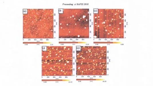
Figure 2 shows the AFM images of the Ino.5Gao.5As/GaAs single layer structure with different growth time for the Ino.5Gao.5As quantum dots. As seen in Figure 2 (a), growth time of 2.0 seconds of Ino.sGao sAs on GaAs buffer layer resulted in the formation of highly uniform islands with small sizes along the steps of the vicinal substrate. The mean size of the islands is 18 nm wide and 5 nm high and the density of the islands on the surface is 3.82 x 1010 cm"2. By interpreting size and the uniformity of the islands, it is suggested that this was the initial stage of islands formation where islands are likely to be coherent. Figure 2 (b) shows that by increasing the growth time to 2.5 seconds, few large islands starts to appear. The formation of the large island is due to coalescence of small islands during the prolonged time. The mean size of the small islands is 18 nm wide and 4 nm high and the density is 4.6 x 1010 cm"2 while the mean size of the large islands is 40 nm wide and 16 nm high and the density is 2.0 x 109cm"2. The increase of small islands density shows that nucleation of new islands take place when the growth time increase indicating that the newly deposited material did not only attach itself to the islands that were already on the surface but also creates hew islands. These were in agreement with the previous study whereby density of islands continues to increase until saturation value as the amount of deposition increases [10]. There is also a possibility that these large islands could also be enlarged by the newly deposited material since the islands that are already formed on the surface are more attractive as it has lower energy.
(a) Repeat stack 5
Proceeding! o/RAFSS 2010
Figure 2: AFM image of the surface morphology of Ino.5Gao.5As/GaAs grown with different growth time :(a) 2.0 , (b) 2.5, (c) 3.0, (d) 3.5 and (e) 4.0 seconds
By lengthening the growth time further to 3.0 seconds resulted in a higher amount of large islands and medium islands replaces small islands as seen in Figure 2(c). The mean size of the islands is 34 nm wide and 17 nm high and the density is 1.26 x 1010 cm2. The decrease in the density value suggests that the small islands have coalesces into each other to form larger islands. Beside that, it can also be noted that the newly deposited material were no longer nucleating at new sites and they attach to the islands which were already on the surface since there were no more small islands appearing. This is also supported by the fact that the density of the islands drops as compared to the sample with Ino.5Gao.3As grown for 2.5 seconds.
For sample with Ino.5Gao.5As grown for 3.5 seconds, the AFM image is shown in Figure 2(d) where non-uniform size distribution clearly can be observed. Ensemble of various size islands identified as small, medium and large islands are present. The presence of small islands suggests that the newly deposited materials were nucleating on new sites because as seen in Figure 2(c), these small islands were not present during growth for 3.0 seconds. This is also supported by the increase in the value of density which is 2.56 x 1010 cm"2. Nevertheless, earlier formed islands were still coalescing with each other as verified by the increase of the size of the islands and the number of these enlarged islands. From Figure 2(e), it can be seen that sample with Ino.sGao sAs grown for 4.0 seconds shows almost a similar surface where growth of islands with non-uniform size distribution takes place. Beside that, the island density shown is 2.92 x 1010 cm"2 and is not much different to the sample grown for 3.5 seconds. This indicates that the rate of nucleation of new islands slows down and most of the newly deposited material attaches themselves to the islands already on the surface. As deposition incr eases, the rate of new islands nucleation decreases and eventually saturates [10] and further deposition will only contribute to the wetting layer and island ripening [11]. Also noted in the AFM image, most of the islands are maintaining the size as they were about the same size as grown for 3.5 seconds. Theoretically, the size of the islands will grow limitedly due to the interaction between the islands [12]. In this case, since the density of the quantum dots is relatively high, the interactions between the islands are accountable for limiting the growth of the size of the quantum dots. Further deposition will be expected to be contributing to the wetting layer and the ripening of the quantum dots upon reaching their critical size since the density will eventually saturate.
Proceeding! o/RAFSS 2010
Figure 3 shows the RT-PL spectra for die samples with five-stacked Iiio.jGao.jAs quantum dots grown for 2.0,2.5,3.5, and 4.0 seconds. For sample grown for 2.0 seconds, the RT-PL spectrum shows only one peak at 1063 nm which is attributed to the small uniform islands as shown in the AFM image in Figure 2(a). Previous reports have seen main peaks emerging at 900 - 950 nm for InGaAs quantum dots grown on GaAs [14,15] for PL measurement at 77 K. However, there wet* also peaks at higher u lOSO nm iad i i s o &m for m m r ^ m ^ m m PL aa&su&aiftia of Eao.6jGao.33As quantum dots [16]. Another room temperature PL extracted from InGaAs quantum dots peak was obtained in the range of
1070 nmto 1160 nm. In the same report, the PL peak was shifted towards lower wavelength as deposition increases [17],
The RT-PL spectrum for stacked sample of Ino.jGao.jAs quantum dots grown for 2.5 seconds shows a main peak that is slightly broaden and is slightly red-shifted to about 1080 nm. The small shift indicates that the size of die small dots did not differ much from the one grown for 2.0 seconds and this is in agreement with the AFM image previously analysed. Another peak on the right side of-the wavelength axis is suggested to be die feature of-the large quantum dots as present in the AFM image. The peak surfaces at about 1270 nm and the intensity is comparatively low indicating that the density of these large islands is also comparatively low. This is also in agreement with the AFM image. In the previous report of Ino.jGao.jAs quantum dots strcuture, bimodal peak were also obtained at about I17Qnm and 99Q nm attributing from two sets of different size quantum dots [18]. The value differs from the one obtained in this experiment as the structure in their report involves AlAs suppressing layer and another strain reducing layer which may have alter their optical properties.
For stacked samples of Ino.jGao.jAs grown for 3.5 and 4.0 seconds, almost very similar spectra were obtained. There were more peaks appearing indicating greater variation of ensemble quantum dots sizes beside the one at 1080 nm. As referred to the AFM images of the single layer uncapped samples, both samples would have non-uniform sized quantum dots and this is approved by the PL spectra obtained. There was also a shoulder peak beside die main peak at 960 nm indicating possibly smaller quantum dots which are of higher energy sub-band [19]. In their report, die dots with higher energy sub-band gave peaks at 980 nm and 1060 nm and this were almost similar to the one obtained in this thesis. It is suggested that these smaller quantum dots are the new quantum dots that nucleate as growth time increases as explained earlier by the AFM analysis. This quantum dots may not have enough time to further enlarge as capping process took place right after the deposition of the Ino.jGao.jAs quantum dots. Therefore these newly formed quantum dots are relatively small to the quantum dots that contributes to the main peaks thus producing a peak which shoulder at lower wavelength value. The main peak and the peak for large quantum dots is found to be at the same value of wavelength signifying that the size of the early formed islands and the large islands to be maintained. However, the intensity of these peaks has increased which denotes an increase of their density. The same trend of size preservation and density increment is seen in the AFM image.
[image:5.594.237.380.505.703.2]From the PL spectra, the main peak that emerges from the quantum dots ensembles with the highest density on the surface is in the range of 1060 - 1080 nm. However, there were also peaks at higher wavelength (1270 nm) which is attributed to the ensemble of larger quantum (tots. The quantum dots buried in die stacked layer shows similarity with die surface quantum dots as seen in the AFM images. It is suggested that for the application of high-wavelength devices, die dots required are large dots with higher density and uniform size. However, large dots are bound to be defective which will be ineffective in any case [10]. Possible approach in tuning the emission to a higher wavelength can be done by exploiting different technique of embedding the quantum dots [4,20].
Figure 3: Room-temperature photoluminescence spectra of stacked taojGaosAs quantum dots structure grown with various growth times
1 1 -i 1 80S 1000 1200 1400
Proceeding! o/RAFSS 2010
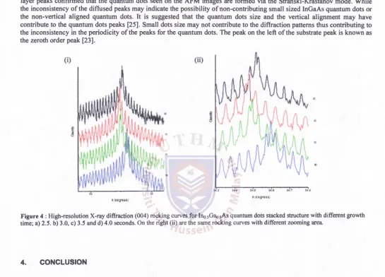
Highly symmetrical rocking curves were obtained for the stacked samples of Ino.5Gao 5As quantum dots grown with different growth time as shown in Figure 4. All of the samples show good quality of stacking indicated by the narrow satellite peaks in a symmetrical envelope function and the long range orders of the satellite peaks [21, 22], The long range order shows uniform strains along [100] plane [23]. In the case of InGaAs quantum dots stacked structure, the narrow satellites peaks are due to the InGaAs wetting layer and the small diffused peaks are due to the InGaAs quantum dots. However, broad peaks may also be attributed to the distortion of the lattice and the imperfection formation [24] . The wetting layer peaks confirmed that the quantum dots seen on the AFM images are formed via the Stranski-Krastanov mode. While the inconsistency of the diffused peaks may indicate the possibility of non-contributing small sized InGaAs quantum dots or the non-vertical aligned quantum dots. It is suggested that the quantum dots size and the vertical alignment may have contribute to the quantum dots peaks [25]. Small dots size may not contribute to the diffraction patterns thus contributing to the inconsistency in the periodicity of the peaks for the quantum dots. The peak on the left of the substrate peak is known as the zeroth order peak [23].
4. CONCLUSION
The most uniformly grown sample for Ino 5Gao 5 As/GaAs was the one grown at 525°C for 2.0 seconds. The islands were also small and have high density. The photoluminescence of the sample shows a peak at 1063nm. Multimodal peak were obtained for the sample with multimodal sized Ino jGaosAs quantum dots. The main peaks were in the range of
1063nm to 1080nm while there were also peaks at 960nm and 1270nm. High-resolution x-ray diffraction measurement for both InAs and Ino.5Gao.5As samples show high quality stacked structure. The I n0 5G a o5A s quantum dots structure has been observed to be suitable for laser application since it has luminescence properties at high wavelength (1270nm). However, the intensity and the multimodal peaks were still not of interest. Thus, further investigation can be done to enhance the luminescence properties. Beside that, other technique in enhancing the luminescence properties such as implementing different capping technique and stacking technique may provide better luminescence at higher wavelength for Ino.5Gao.5As
[image:6.596.28.573.150.542.2]quantum dots.
Figure 4 : High-resolution X-ray diffraction (004) rocking curves for Ino 5Gao.sAs quantum dots stacked structure with different growth time; a) 2.5. b) 3.0, c) 3.5 and d) 4.0 seconds. On the right (ii) are the same rocking curves with different zooming area.
Proceedings ofRAFSS 2010
ACKNOWLEDGEMENT
Financial support by the Ministry of High Education Malaysia is gratefully acknowledged. Acknowledgements also to Institute of Ibnu Sina and Department of Physics, Faculty of Science, Universiti Teknologi Malaysia for providing space and equipments for laboratory works. Universiti Tun Hussein Onn Malaysia is also acknowledged for providing scholarship to the author.
REFERENCES
[ 1.] Alexander A. Balandin and K.L. Wang, eds. Handbook of semiconductor nanostructures and nanodevices 2006, Stevenson Ranch, CA:
American Scientific Publishers.
[2.] Ayers, J.E., Heteroepitaxy af semiconductors: theory, growth, and characterization. 2007, United States of America: CRC Press, Taylor and
Francis Group.
[3.] Mitin, V. V., V.A. Kochelap, and M.A. Stroscio, Introduction to rumoelectronics: Science, nanotechnology, engineering and application. 2008,
United States of America: Cambridge University Press, New York.
[4.] Passaseo, A., V. Tasco, I. Tarantini, M. De Giorgi, M.T. Todaro, M. De Vittorio, and R. Cingolani, Tuning of long-wavelength emission in
IthGai-xAs quantum dot structures. Physica E: Low-Dimensional Systems and Nanostructures, 2004. 23(3-4): p. 390-395.
[5.] Germann, T.D., A. Strittmatter, T. Kettler, K. Posilovic, U.W. Pohl, and D. Bimberg, MOCVD of InGaAs/GaAs quantum dots for lasers
emitting close to 1.3 [mu]m. Journal of Crystal Growth, 2007. 298: p. 591-594.
[6.] Chyi, J.-I., MBE growth and characterisation of InGaAs quantum dot lasers. Material Science and Engineering, 2000. B 7:5: p. 121-125. [7.] AbuWaar, Z.Y., E. Marega Jr, M. Mortsravi, and GJ. Salarao, In situ photohtmmescnce study of uncapped InAs/GaAs quantum dots.
Nanotechnology, 2008.19: p. 335712.
[8.] Sellin, R.L., C. Ribbat, M. Grundmann, N.N. Ledentsov, and D. Bimberg, Close-to-ideal device characteristics of high-power InGaAs/GaAs
quantum dot lasers. Applied Physics Letters, 2001. 78(9): p. 1207-1209.
[9.] Aryanto, p., Z. Othaman, S. Roslan, UK. Boo, R. Muhammad, and A.S. Ameruddin Effect of buffer layer thickness on the surface morphology
of lnaisGao ssAs epitaxylayer grown by MOCVD. in The regional Annual Fundamental Science Seminar (RAFSS). 2008. UTM, Malaysia.
[10.] Lever, P., Interdiffusion and metalorganic vapour phase epitaxial growth of self-assembled InGaAs quantum dot structures and devices. 2004,
The Australian National University: Australia
f 11.] Barabasi, A., Thermodynamic and kinetic mechanisms in self-assembled quantum dot formation. Materials Science and Engineering, 1999. B67:
p. 23-30. '
[12.) Li, X.L., G. Ouyang, and G.W. Yang, A thermodynamic theory of the self-assembly ofquantum dots. The open-access journal for physics, 2008:
p. 1-14.
[13] Hsieh, T.-P., H.-S. Chang, W.-Y. Chen, W.-H. Chang, T. Hsu, N.-T. Yeh, W.-J. Ho, P.-C. Chiu, and J.-I. Chyi, Growth of low density InGaAs
quantum dots for single photon sources by metal-organic chemical vapour deposition. Nanotechnology, 2006.17: p. 512-515.
[14.] Saravanan, S. and H. Shimizu, Long wavelength and narrow photoluminescence linewidth from InAs quantum dots with GaAs cap layer on
GaAs (1 0 0) substrate. Journal of Crystal Growth, 2006.289(1): p. 14-17.
[15.] Yu, L.K., B. Xu, Z.G. Wang, P. Jin, C. Zhao, W. Lei, J. Sun, K. Li, L.J. Hu, and L.Y. Liang, The effect of In content on high-density
InxGal-xAs quantum dots. Journal of Crystal Growth, 2005.282(1-2): p. 173-178.
[16.] Sellin, R., U.W. Pohl, D. Bimberg, I. Kaiander, D. Ouyang, T. Kettler, N. Zakharov, and P. Werner, Alternative-precursor metalorganic
chemical vapor deposition of self-organized InGaAs/GaAs quantum dots and quantum-dot lasers. Appl. Phys. Lett., 2003.82(6): p. 841-843.
[17.] Heinrichsdorff, F., A. Krost, M. Grundmann, D. Bimberg, F. Bertram, J. Christen, A.O. Kosogov, and P. Werner, Self organization phenomena
of InGaAs/GaAs quantum dots grown by metalorganic chemical vapour, deposition. Journal of Crystal Growth, 1997.170(568-573).
[18.] Lan, Q., Z.C. Niu, D.Y. Zhou, Y.C. Kong, XD. Wang, Z.H. Miao, and S.L. Feng, Surface morphology and optical property of 1.3 /Jm
InojGaasAs/GaAs self-organized quantum dots grown by MBE. Physica E: Low-Dimensional Systems and Nanostructures, 2003.17: p.
114-116.
[19.] Kitamura, M., M. Nishioka, R. Schur, and Y. Arakawa, Direct observation of the transition from a 2D layer to 3D islands at the initial stage of
InGaAs growth on GaAs by AFM. Journal of Crystal Growth, 1997.170: p. 563-567.
[20.] Saint-Girons, G., G. Patriarche, L. Largeau, J. Coelho, A. Mereuta, J.M. Gerard, and I. Sagnes, Metal-organic vapor-phase epitaxy of
defect-free InGaAs/GaAs quantum dots emitting around 1.3 fan. Journal of Crystal Growth, 2002.235(1-4): p. 89-94.
[21.] Mazur. Y.I., Z.M. Wang, and G.J. Salamo, Investigation of inditim distribution in InGaAs/GaAs quantum dots stacks using high resolution
x-ray diffraction and Raman scattering Journal of Applied Physics, 2006.99: p. 023517.
[22.] Wang, H., S.J. Xu, L. Qing, and S.L. Feng, X-ray diffraction Analysis on Gallium-Indium interdiffusion in quantum dots suoerlattices. Chin.
Phys. Lett., 2001.18(6): p. 810.
[23.] Sagnes, I., I. Prevot, G. Patriarche, G. Le Roux, B. Gayral, A. Lemaltre, and J.M. Gerard, High-quality InAs/GaAs quantum dots grown by
low-pressure metalorganic vapor-phase epitaxy. Journal of Crystal Growth, 1998.195(1-4): p. 524-529.
[24.] Ng, J., U. Bangert, and M. Missous, Defect investigation of stacked self-assembled InAs/GaAs quantum dot lasers. Phys. Stat. Sol. (c), 2007.8:
p. 2986-2991.