Gating Technique in Different CMOS Design Style at
45Nanometer Regime
Bhanupriya Bhargava
Research Scholar, ITM Gwalior, IndiaPradeep Kumar Sharma
Research Scholar, ITM Gwalior, IndiaShyam Akashe
Associate Professor,ITM Gwalior, India
ABSTRACT
As transistor sizes scale down and levels of integration increase, leakage power has become a vital downside in modern low-power VLSI technology. This is often very true for ultra-low- voltage (ULV) circuits, wherever high levels of leakage force designers to selected relatively high threshold voltages, which limits performance. In this paper, we design different design approach of master slave D flip-flop with stacking power gating leakage reduction technique. Here these techniques essentially increase the effective resistance of leakage paths by adding sleep transistors between logic stacks and power supply rails. Power gating technique also provides many of the property from transistor stacking technique. The proposed approach saves maximum amount of the Leakage power without degrading the performance of the circuit. In this work we analyses the leakage power of three different types of CMOS design style such as pass transistor logic (PTL), transmission gates and gate diffusion input (GDI) design. All these proposed circuits are simulated with and without the application of leakage reduction techniques. The circuits are simulated using Cadence Virtuoso tool at 45nm technology for various parameters.
Keywords
Low power VLSI, pass transistor logic (PTL).transmission gate, gate diffusion input (GDI), master slave flip flop, leakage power, stacking power gating technique
1.
INTRODUCTION
Now a day low-power electronics devices such as laptops, computer, mobile phone power consumption has become major concern in VLSI design. The betray lifetime of such devices is nice concern. When mobile phone is operated in standby mode, bound programs of mobile phone are turned off throughout active mode but this does not stop the battery from obtaining depleted [1][2]. This is because circuits which are de- activated by turning off bound programs still have discharge currents flowing through them. although the magnitude of leakage current is lesser than the conventional operational current but leakage current erodes battery life over comparatively long standby time whereas the conventional operational current erodes battery life over comparatively short speak time. So this is often why low power circuits for mobile applications are of great interest [3] [4] [5]. Implementation of master slave D flip flop to reduce the power consumption and to increase the speed has proved to be a worthy solution towards power reduction. Moreover, realization of master slave flip flop with CMOS transmission gate for achieving high speed ,along with lower power and area [6] [7] . The Performance of the master slave flip flop can be evaluated by
measuring the factors such as leakage power, active power, and delay of the proposed circuit. Integrated circuit power dissipation consists of various components depending on the circuit operating mode. First, the switching or dynamic power element dominates throughout the active mode of operation and other there are two primary leakage sources, the active leakage component and the standby leakage component. The standby leakage could also be created by significantly smaller than the active leakage by changing the body bias conditions or by power-gating [8] [9] [10].
Many leakage reduction techniques are present reduce leakage power in the circuit at significant level. Power Gating has become one of the most widely used circuit design techniques for reducing leakage current in Static power dissipation [11][12]. This paper concentrates on reduction of leakage power which occurs during the transition from sleep mode to active mode. In this paper design low power master slave D flip flop using various CMOS design style such as pass transistor, transmission gate and GDI method. These all master slave D flip flops has been realized with stacking power gating leakage reduction technique in 45 nanometer technology.
2.
PROPOSED STACKING POWER
GATING TECHNIQUE
Fig 1: stacking power gating technique
3.
CMOS IMPLEMENTATION OF D
FLIP-FLOP CIRCUITS
In every digital circuit latches and Flip-Flops are most commonly used memory storage element. These memory storage elements are used for storing information. One latch or flip-flop can be capable to store one bit of information .This section present the implementations of three different design style of CMOS technology which is used to design the D flip-flops circuits. These flip-flop circuits are combined pair of master and slave D latch circuit.
3.1
Implementation of pass Transistor
Logic (PTL) based D Flip-Flop Circuit
It is confirmed that pass transistor based CMOS logic can be frequently utilized where high speed and high packaging
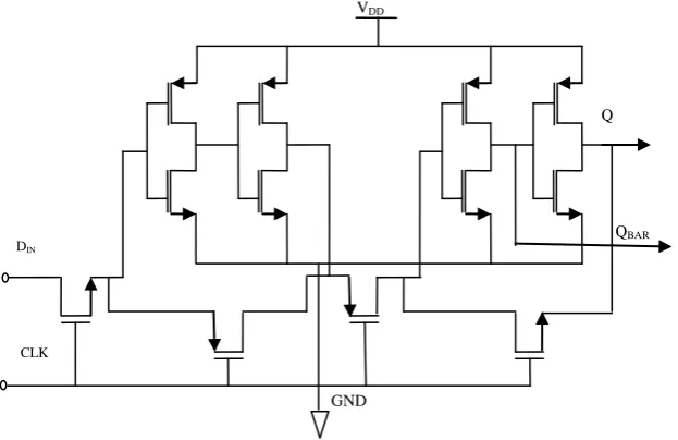
density is a major concern. The logic results in reduction in the number of transistors of the circuit by introducing differential logic and eliminating additional transistors. In pass transistor logic [16] style we use either NMOS or PMOS transistor to build a design. Logic levels are passed between nodes of circuit as transistors are utilized as switches. The amount of active devices is thus reduced; however as the number of stages increase it becomes difficult to observe a significant difference between high and low logic levels [17] [18]. Master-slave latches have been implemented using inverters and pass transistor logic (PTL) as shown in figure2. The two chained inverters are in memory state when the PMOS loop transistor is on, that is when clock (clk) = 0. Other two chain inverters on the right hand side acts in the opposite way. The flip-flop changes its state during the falling edge of the clock.
Fig 2: D flip-flop using Pass transistors
DIN
CLK
Q VDD
GND
QBAR
Pull-up
Network
Pull-down
Network VDD
GND
INPUT OUTPUT
SLEEP
[image:2.595.143.455.503.705.2]based D Flip- Flop Circuit
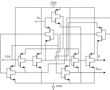
Transmission gate and inverters are utilized to implement D flip-flop circuit as illustrated in Figure 3 shows. Transmission gate is a most commonly used CMOS structure for implementing integrated circuits that maintains switch function, efficient layout and logic reduction [19] .In figure 3 transmission gates T1 and T4 are turned ON and transmission
[image:3.595.137.450.187.410.2]T4. The value from Din, triggered previously, is kept within the slave at this time. At this stage master latches next state, but as T3 is OFF it does not reaches slave. T2 and T3 are turned ON at the positive edge of clock which latches the value to reach to slave through the loop of inverters P1, P2 and T2 [20].
Fig 3: D flip-flop using transmission gates
3.3
Implementation of GDI based D Flip-
flop Circuit
The GDI approach allows implementation of a wide range of complex logic functions using only two transistors. This method is suitable for design of fast, low-power circuits, using a reduced number of transistors (as compared to CMOS and existing PTL techniques), while improving logic level swing and static power characteristics and allowing simple top-down design by using small cell library. The GDI method is based on the use of a simple cell as shown in Figure4 (a).
Representation of two GDI based latches connected as master-slave configuration is illustrated in Figure 4(b). The state of circuit during period of operation is due to the body gates. The gates make two different paths and are confirmed by the clock (clk) signal. The first one is for transparent latch state, given that clock is low PMOS transistor is propagating the signals. The second one is for hold latch state, provided that the clock is high values of internal circuit is sustained because of NMOS transistors [20] [21] [22]. The complementary value in the internal signals and outputs is maintained by the inverters.
G
P
OUT=G’P+GN
DIN
Q
GND
P1 P2 P3 P4
T1
T2
T3
T4 VDD
CLK
[image:3.595.190.399.568.743.2]Fig 4(b): D flip-flop using GDI gates
4.
SIMULATION AND RESULT
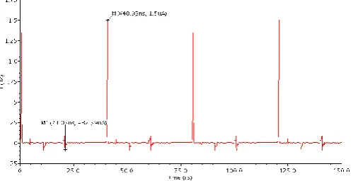
Figure 5 show input output waveform of the D Flip-Flop circuit. The following waveform shows the Active power and leakage current of the proposed circuits with using of stacking power gating leakage reduction technique. The obtained result of active and leakage power of D flip-Flop circuits with and without using of proposed stacking technique are presented in table1 and 2. Figure 6(a) and 6(b) respectively show active
[image:4.595.117.478.79.373.2]current of the circuit and leakage current waveform of PTL based DFF using stacking technique. The active current and leakage current for the transmission gate based D flip flop has beenshown in figure 7(a) and 7(b). Figure 8(a) and 8(b) show the same parameters of GDI based DFF using stacking technique.
Fig 5: Input Output waveform of D Flip Flop
DIN
CLK Q
QBAR VDD
[image:4.595.133.454.490.702.2]Conventional DFF Design using Active Power Leakage Power
PASS Transistors logic 426.0nw 297.1nw
Transmission Gate 41.55nw 13.87pw
[image:5.595.159.434.86.208.2]Gate Diffusion Input (GDI) 40.25nw 10.1pw
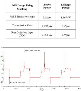
Table 2 show Active and Leakage power of D Flip-Flop using stacking power gating Technique based Circuits
DFFDesign Using Stacking
Active Power
Leakage Power
PASS Transistors logic 2.65µW 1.567nW
Transmission Gate 2.237 µW 3.99pw
Gate Diffusion Input
(GDI) 2.053 µW 2.59pw
[image:5.595.162.431.237.539.2] [image:5.595.157.434.582.731.2]Fig 7(a): Active Current of Transmission Gate based DFF using with Stacking Technique
Fig 7(b): Leakage Current of Transmission Gate based DFF using with Stacking Technique
[image:6.595.160.430.100.246.2] [image:6.595.157.435.283.434.2] [image:6.595.172.422.476.604.2]Fig 8(b): Leakage Current of GDI based DFF using with Stacking Technique
5.
CONCLUSION
In this paper we present designed and analysis of different CMOS logic style such as pass transistor logic, transmission gate and gate diffusion input (GDI) using with stacking power gating leakage reduction technique. As an observation result the stacking technique is more suitable technique for reducing maximum leakage power in all CMOS logic style. On the basis of simulation results the GDI based designed topology is suitable for designing high speed low power devices. Another advantage of this CMOS style it’s providing greater design flexibility as compared to other design style. These all results were obtained on “cadence virtuoso tool” using specter simulator at 45nm CMOS technology and operated supply voltage is .7V.
6.
ACKNOWLEDGMENT
This work was supported by ITM University Gwalior, with collaboration Cadence Design System, Bangalore.
7.
REFERENCES
[1] A.G.M. Strollo, E. Napoli, D. De Caro,” New Clock-Gating Techniques for Low-Power Flip-flops,”low power electronics and design ISLPED, pp.114-119, 2000.
[2] Richa Singh, Rajesh Mehra,” Power efficient design of multiplexer using adiabatic logic,” international Journal of Advances in Engineering & Technology, Mar. 2013.
[3] Shyam Akashe, Sushil Bhushan, Sanjay Sharma,” High Density and Low Leakage Current Based 5T SRAM Cell Using 45 nm Technology,” Romanian journal of information science and technology ,vol.15,pp.155-168,2012.
[4] Shyam Akashe, Rashmi Bahal ,Sanjay Sharma, ”Leakage power minimization in SRAM by using standby voltage,” Journal of computational and theoretical nanoscience,Vol.9,pp.1040-1043,2012.
[5] Amit Bakshi ,”Implimentation of power gating technique in CMOS full adder cell to reduce leakage power and ground bounce noise for mobile application,” International Journal of Electronics, Communication &
[6] C.N Marimuthu, P.Thangaraj,” Transmission gate based high performance low power multiplier,” journal of applied sciences,Vol. 10,2010.
[7] D.Radhakrishnan,” Low-voltage low-power CMOS full adder,” IEE Proc.-Circits Devices Syst., Vol. 148, Februirry 2001.
[8] Farzan Fallah, Massoud Pedram,” Standby and Active Leakage Current Control and Minimization in CMOS VLSI Circuits,”IEICE Transactions,pp.509-519, 2005.
[9] Shyam Akashe, Sanjay Sharma,”Leakage Current Reduction Techniques for 7T SRAM Cell in 45 nm Technology,” Wireless Personal Communication, august 2012.
[10]Manish Dev Singh, Shyam Akashe,Sanjay Sharma,” Leakage power reduction techniques of 45 nm static random access memory (SRAM) cells,” International Journal of the Physical Sciences ,Vol. 6, pp. 7341 - 7353, December 2011.
[11]S. Anvesh,P. Ramana Reddy,” Optimized Design of an Alu Block Using Power Gating Technique,” IOSR Journal of Electronics and Communication Engineering (IOSR-JECE) Vol 4, PP 24-30, Dec. 2012.
[12]Saurabh Khandelwal, Shyam Akashe,Sanjay Sharma, ”Supply voltage minimization techniques for SRAM leakage reduction,” Journal of computational and theoretical nanoscience,Vol.9,pp.1044-1048,2012..
[13]Anita Lungu, Pradip Bose, Alper Buyuktosunoglu, and Daniel J. Sorin,” Dynamic Power Gating with Quality Guarantees,” International Symposium on Low Power Electronics and Design ,2009.
[14]Kaijian Shi, David Howard “Sleep Transistor Design and Implementation – Simple Concepts Yet Challenges To Be Optimum” VLSI Design, Automation and Test, International Symposium, 2006.
[image:7.595.144.448.71.235.2][16]M. V. D. L. Varaprasad, Rohit Bapna, Manisha Pattanaik, “Performance Analysis of Low leakage 1- bit Nano-CMOS Based Full Adder Cells for Mobile Applications, ” Proceedings of International Conference on VLSI Design & Communication Systems, pp.233-238, January 2010.
[17]J. B. Kuo and J. H. Lou, “Low-Voltage CMOS VLSI Circuits”, John Wiley: New York, 1999.
[18]Doshi N. A, Dhobale S. B, and Kakade S.R,“LFSR Counter Implementation in CMOS VLSI”, World Academy of Science, Engineering and Technology, 2008.
[19]WEIZE XU AND EBY G. FRIEDMAN,” Clock Feedthrough in CMOS Analog Transmission Gate
Switches” Analog Integrated Circuits and Signal Processing, 44, 271–281, 2005
[20]Po-Ming Lee, Chia-Hao Hsu, and Yun-Hsiun Hung,” Novel 10-T full adders realized by GDI structure,” Integrated Circuits, ISIC, pp.115-118, 2007.
[21]Morgenstein, A.Fish, I.Wagner, “A Efficient Implementation of D Flip- Flop Using the GDI Technique”, ISCAS’04, pp.673-676, 2004.