HR-04027
For FCC information, please contact your Cray Research account manager.
Autotasking, CRAY, CRAY-1, Cray Ada, CRAYY-MP, HSX, SSD, UNICOS, and X-MP EA are federally registered trademarks and CCI, CF77, CFT, CFf2, CFT77, COS, CRAYX-MP, CRAYXMS, CRAY-2, CRl/TurboKiva, CSIM, CVT, Delivering the power ... , Docview, IDS, MPGS, OLNET, RQS, SEGLDR, SMARTE, SUPERCLUSTER, SUPERUNK, Trusted UNICOS, UniChem, Y-MP, and Y-MP C90 are trademarks of Cray Research, Inc.
Ethernet is a trademark of Xerox Corporation. EXABYTE is a trademark of EXABYTE Corporation. HYPERchannel and NSC are trademarks of Network Systems Corporation. SPARC is a trademark of SPARC International, Inc. UNIX is a trademark of UNIX System Laboratories, Inc.
Requests for copies of Cray Research, Inc. publications should be directed to:
CRAY RESEARCH, INC. Distribution
2360 Pilot Knob Road Mendota Heights, MN 55120 (800) 284-2729 extension 5907
Comments about this publication should be directed to: CRAY RESEARCH, INC.
Hardware Publications and Training 770 Industrial Blvd.
Each time this manual is revised and reprinted, all changes issued against the previous version are incorporated into the new version, and the new version is assigned an alphabetic level which is indicated in the publication number on each page of the manual.
Changes to part of a page are indicated by a change bar in the margin directly opposite the change. A change bar in the footer indicates that most, if not all, of the page is new. If the manual is rewritten, the revision level changes but the manual does not contain change bars.
REVISION
001
DESCRIPTION
Original printing. January 1992.
August 1992. This change packet updates the DAS-2 disk array
This manual is written primarily for customers of Cray Research, Inc. and describes the basic functions of the CRAY Y-MP EL system manufactured by Cray Research. It also describes the design and architecture of the CRAY Y -MP EL system and its associated peripheral devices.
•
•
•
Section 1 provides an overview of the major components of a CRAY Y-MP EL system.
Section 2 describes the major functional areas of the CPU and provides a summary of the CPU instruction set.
Section 3 describes the input/output subsystem (IDS) and system peripherals.
Each section has a separate table of contents.
Please use one of the reader comment forms located at the front and back of this manual to suggest improvements or to point out technical errors. The following conventions are used throughout this manual.
Convention Lowercase italic Xorx orx n
(value)
Register bit
Description
Variable information. An unused value. A specified value.
The contents of the register or memory location designated by value.
Convention Designators
Number base
Description
Bit 2° corresponds to the least significant bit of the register. One exception is the vector mask register. The vector mask register bits
correspond to a word element in a vector register; bit 263 corresponds to element 0 and bit 2° corresponds element 63. All numbers used in this manual are decimal unless otherwise indicated. Octal numbers are indicated with an 8 subscript. Exceptions are register numbers, instruction parcels in instruction buffers, and instruction forms, which are given in octal without subscript notation.
The following are examples of the preceding conventions. Example
Transmit (Ak) to Si
167ixk
Read n words from memory
10008
Description
Transmit the contents of the A register specified by the k field to the S register specified by the "i field.
Machine instruction 167. The x represents the j field, which is not used. Read a specified number of words from memory.
The value represents the most
significant bit of an S register or element of a V register.
1 SYSTEM OVERVIEW
2 CPU
Mainframe Cabinet ... 1-1 Peripheral Cabinet . . . 1-3 Disk Subsystems ... 1-3 Tape Subsystems
Maintenance Workstation Power and Cooling Network Interfaces
System Software ... . System Configurations ... .
1-4
1-4
1-4
1-4
1-5
1-5
CPU Control Section. . . .. . . . .. . . 2-26
Exchange Mechanism ... 2-26
Exchange Sequence. . . 2-26
Exchange Package. . . 2-26
Instruction Fetch. . . 2-32
Instruction Issue .. . . 2-32
Programmable Clock ... 2-33
Status Register ... 2-33
Special Features of the CPU ... 2-33
Pipelining and Segmentation. . . 2-34
Functional Unit Independence . . . 2-34
Vector Processing . . . 2-35
Definition of Vector Processing ... 2-36
Advantages of Vector Processing ... 2-36
Vector Chaining. . . 2-36
Types of Vector Instructions ... 2-38
Instruction Formats ... 2-45
1-parcel Instruction Format with Discrete j and k
Fields ... 2-45
1-parcel Instruction Format with Combined j and k
Fields ... 2-46
2-parcel Instruction Format with Combined j, k, and m
Fields ... 2-46
2-parcel Instruction Format with Combined ~ j, k, and m
Fields ... 2-47
3-parcel Instruction Format with Combined
m
andn
Fields ... 2-48
Instruction Differences between X-mode and Y -mode. . . 2-49
Special Register Values . . . 2-50
Monitor Mode Instructions. . . 2-51
Special CAL Syntax Forms . . . 2-51
CPU Instruction Summary ... 2-52
Memory Transfer Instructions. . . 2-59 Integer Arithmetic Instructions . . . 2-63 Floating-point Arithmetic Instructions ... 2-65 Logical Operation Instructions ... 2-68 Shift Instructions . . . 2-72 Bit Count Instructions . . . 2-73 Branch Instructions ... . . . 2-7 4 Monitor Mode Instructions ... . . . 2-7 6
3 INPUT/OUTPUT SUBSYSTEM
IDS Configurations ... 3-1 Channel Communications and Networking ... 3-2 Master I/O Processor . . . 3-3 Peripheral Devices . . . 3-3 DD-3 Disk Drive ... 3-3 DC-3 Disk Controller . . . 3-4 DD-4 Disk Drive ... 3-4 DC-4 Disk Controller . . . 3-4 DAS-2 Disk Array Subsystem . . . 3-4 DAS-2 Disk Array Subsystem Controller ... 3-5 DEB-2 Disk Array Bank ... 3-5 RD-1 Removable Disk Subsystem . . . 3-5 RD-2 Removable Maintenance Drive ... 3-5 TD-2 Tape Drive Subsystem ... 3-5 TC-2 Tape Controller . . . 3-6 TD-3 Tape Drive Subsystem ... 3-6 SI-1 Small Computer System Interface ... 0 3-6
EX-2 8nim Cartridge Tape Subsystem. 0 • • 0 • • • • • • • • • • 3-6
Network Connections ... · 0 • • • • • • • • • • • • • • • • • • • • • 3-6
Ethernet Interface Controller 0 • 0 • • • • • • • • • • • • • 3-6
Fiber-optic Distributed Data Interface Controller 3-7 HYPERchannel Interface Controller. 0 • • • • • • • • 3-7
BIBLIOGRAPHY
INDEX
FIGURES
Bibliography ... Bib-1
Index ... Ind-1
Figure 1-1.
Figure 1-2.
Figure 2-1.
Figure 2-2.
Figure 2-3.
Figure 2-4.
Figure 2-5.
Figure 2-6.
Figure 2-7.
Figure 2-8.
Figure 2-9.
CRAY Y-MP EL Computer System ... .
Example of Cabinet Layout for the CRAY Y-MP EL System ... .
CRAY Y-MP ELSystem CPU Block Diagram .. .
Integer Data Formats ... .
24-bit Integer Multiply Performed in
Floating-point Mulitply Functional Unit ... .
32-bit Integer Mulitply Performed in
Floating-point Mulitply Functional Unit ... .
Floating-point Data Format ... .
Internal Representation of Floating-point Number
Biased and Unbiased Exponent Ranges ... .
Floating-point Add and Multiply Range Errors .. .
Floating-point Reciprocal Approximation Range Errors ... .
1-2
1-3
2-4
2-13
2-14
2-15
2-16
2-16
2-17
2-18
2-19
Figure 2-10. Newton's Method for Approximating Roots. . . 2-23
Figure 2-11. Segmentation and Pipelining Example ... 2-35
Figure 2-12. Vector Chaining Example ... 2-38
Figure 2-13. Vector-vector Operand Instructions. . . 2-39
Figure 2-14. Vector-scalar Operand Instructions. . . 2-39
Figure 2-15. Vector Memory Instructions ... 2-40
TABLES
Figure 2-19. General Format for Instructions. . . 2-45
Figure 2-20. I-parcel Instruction Format with
Discrete j and k fields ... 2-46 Figure 2-21. I-parcel Instruction Format with
Combined j and k Fields ... 2-46 Figure 2-22. 2-parcellnstruction Format with
Combined j, k, and m Fields ... 2-47 Figure 2-23. 2-parcel Instruction Format with
Combined ~ j,
k,
and m Fields ... 2-48 Figure 2-24. 2-parcel Instruction Format for a 24-bit ImmediateConstant with Combined ~ j, k, and m Fields . . . . 2-48 Figure 2-25. 3-parcel Instruction Format with
Combined m and n Fields ... 2-49 Figure 3-1. lOS Block Diagram. . . 3-2
Table 1-1.
Table 2-1.
Table 2-2.
Table 2-3.
CRAY Y-MP EL System Configurations ... 1-5
3-parcel Instructions ... 2-50
CRAY Y-MP and CRAY X-MP Instruction
Differences. . . 2-50
Mainframe Cabinet
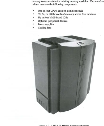
The CRAY Y-MP EL minisupercomputer system (refer to Figure 1-1) makes real supercomputing available to more prospective supercomputer users with its affordable entry-level system. It is easy to install and can be installed in almost any office environment. Each cabinet is air cooled and consumes a maximum of only 6 kW of power.
The CRAY Y -MP EL system is a minisupercomputer system that includes one to four 30-ns central processing units (CPUs), central memory, input/output subsystem (IDS), and disk and tape storage units that are all contained in one mainframe cabinet (cabinet 1). One or more optional peripheral cabinets may contain additional lOSs and optional peripheral devices (cabinets 2, 3, and 4). A typical layout of each of these cabinets is shown in Figure 1-1.
The CRAY Y -MP EL system features the following large-scale supercomputer features:
•
•
•
•
•
•
Vector capability
Parallel processing
Memory capacity of 32, 64, or 128 Mwords that use dynamic random-access memory (DRAM) components
I/O capacity
Powerful and productive software
Use of existing CRAY Y -MP supercomputer applications
The following subsections discuss the mainframe and peripheral cabinet and their components. Section 2 contains a more detailed description of the CPU; Section 3 describes the IDS.
/
may be field upgraded by adding aq.ditional CPU modules and by adding
memory components to the existing memory modules. The mainframe
cabinet contains the following components:
•
•
•
•
•
•
One to four CPUs, each on a single module
32, 64, or 128 Mwords of memory across four modules Up to four VME-based lOSs
Optional peripheral devices Power supplies
[image:15.611.77.517.90.622.2]Cooling fans
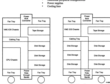
Peripheral Cabinet
Power Bulk Fan Tray Converter
VME IDS Chassis
Cabling Tray
CPU Chassis
Power Fan Tray
Ride-through
o
BanksOne to three peripheral cabinets can be attached to the mainframe when
the system is ordered or as part of an upgrade. Peripheral cabinets may
be added to provide up to 16 lOSs and over 200 Gbytes of disk storage.
A peripheral cabinet can include the following components (refer to
Figure 1-2):
•
•
•
•
Fan Tray Tape Storage Disk Storage Disk Storage Disk Storage Fan Trayo
Up to 12 additional lOSs (up to 16 total for entire system)
Additional peripheral configurations
Power supplies
Cooling fans
Power Bulk
Fan Tray Converter Fan Tray
VME IDS Chassis
Tape Storage
Cabling Tray
Disk Storage Disk Storage
Disk Storage Disk Storage
Disk Storage Disk Storage
Power
Fan Tray Ride- Fan Tray through
Banks
o
o
A·OOM [image:16.620.72.542.202.561.2]Back View of Cabinet 1 Back View of Cabinets 2, 3, and 4
Figure 1-2. Example of Cabinet Layout for the CRAY Y-MP EL System
Disk Subsystems
Tape Subsystems
controls these devices via controller boards. Refer to Section 3 for a description of each disk storage device that is offered as optional equipment with the system.
Cray Research uses other manufacturers' tape drive products for the CRAY Y -MP EL system; the lOS also controls these devices. An
autoloading low-profile 9-track tape drive, lI2-in. cartridge 3480-type tape drive, and an 8-mm helical scan tape system are the tape support options offered with the system. These are described in greater detail in Section 3.
Maintenance Workstation
Power and Cooling
Network Interfaces
The CRAY Y -MP EL system uses a maintenance workstation model EL (MWS-EL) that provides a dedicated platform for performing hardware maintenance and monitoring Cray Research, Inc. computer systems. Cray Research owns the MWS-EL and uses it for offline diagnostic testing, diagnostic listings, and hardware error logging. The MWS-EL is supplied as part of the maintenance contract. The MWS-EL is not part of the customer's system and is not connected to the customer's network. System operators use a system console, rather than an operator workstation (OWS).
The CRAY Y -MP EL system is completely air cooled and requires no raised floor or refrigeration. Fans are located at the top and bottom of each cabinet. Airflow through the frame is vertical, and the air is filtered at the base of the frame.
A power conditioning and distribution system is located in each
mainframe and peripheral cabinet. The CPU and VME components have their own power supplies.
System Software
The following Cray Research, Inc. binary system software is shipped with the CRAY Y -MP EL system:
•
•
•
•
•
•
UNICOS operating system derived from UNIX System Laboratories, Inc. UNIX System V
Cray CF77 FORTRAN compiling system Cray ANSI standard C compiler
Cray Assembly Language (CAL) - a versatile macro assembler
Utilities
Cray subroutine libraries
System Configurations
Customers can upgrade the number of CPUs, size of central memory, number of lOSs, and number and type of peripheral devices. The naming convention for these systems is CRAY Y -MP EL /n-y; nand y represent the following numbers:
n
=
Maximum number of mainframe CPU s the system can contain y=
Central memory size in megabytes (Mbytes); refer to Table 1-1. For example, a CRAY Y-MP EL/4-1024 computer system has four CPUs and 1,024 Mbytes (128 Mwords) of central memory.Table 1-1. CRAYY-MP EL System Configurations
VME Central Memory
Product Name CPUs Memory Size I/O Subsystems (Mbytes)
CRAYY-MP ELJ1-256 1 32 Mwords 1 to 4 256 (32 Mwords)
CRAYY-MP ELJ1-512 1 64 Mwords 1 to 4 512 (64 Mwords)
CRAYY-MP ELJ1-1024 1 128 Mwords 1 to 4 1,024 (128 Mwords)
CRAYY-MP ELJ2-256 2 32 Mwords 1 to 8 256 (32 Mwords)
CRAYY-MP ELJ2-512 2 64 Mwords 1 to 8 512 (64 Mwords)
CRAYY-MP ELJ2-1024 2 128 Mwords 1 to 8 1,024 (128 Mwords)
CRAY Y-MP ELJ4-256 4 32 Mwords 1 to 16 256 (32 Mwords)
CRAYY-MP ELJ4-512 4 64 Mwords 1 to 16 512 (64 Mwords)
This section describes the major functional areas of a CRAY Y -MP EL central processing unit (CPU) and special features of the mainframe. Section 2 also provides a summary of the Cray Assembly Language ( CAL) instruction set.
CPU Shared Resources
Central Memory
The CPUs share several functional areas (or sections) of the mainframe. These sections include central memory, the I/O section, the
interprocessor communication section, and the real-time clock (RTC). The following subsections describe these functional areas.
Central memory is shared by the CPUs and the I/O section. Central memory is divided into sections and banks. This arrangement allows simultaneous and overlapping memory references. Simultaneous references are two or more references that begin at the same time; overlapping references are one or more references that begin while another reference is in progress.
Each CPU in the system has four parallel memory ports. Each port performs specific functions, allowing different types of memory transfers to occur simultaneously. To further enhance memory operations, the bidirectional memory mode allows block read and write operations to occur concurrently.
The mainframe has built-in conflict resolution hardware to minimize the delays caused by memory conflicts and to maintain the integrity of all memory references when conflicts occur. A memory conflict occurs when more than one reference is made to the same area of central memory.
lOS
word. When the word is read from central memory, the checkbyte and data word are processed to determine whether any bits were altered. If
no errors occurred, the word is passed without modification.
If an error occurred, the 8 bits of the checkbyte are analyzed by the logic to fmd the number of altered bits. If only a single bit was altered, the correction logic resets that bit to the correct state and passes the corrected word on. The memory error flag in the exchange package sets to indicate that an error occurred, which can generate an interrupt. (Refer to "Flag Register Field" in this section for more information on the memory error flag.) Error information is also sent to an error logger.
If more than a single bit is altered, the logic cannot correct the word and the results are unpredictable. When a double error is detected, the memory error flag in the exchange package sets to indicate an error occurred, which can generate an interrupt.
Each CPU can be connected to a maximum of four lOSs, each via 40-Mbyte/s channels. These channels are used to transfer data between the CPU and the IDS. Refer to Section 3 for a more detailed description of the IDS.
Interprocessor Communication Section
The interprocessor communication section of the mainframe contains clusters of shared registers for interprocessor communication and synchronization. Each cluster consists of shared address (SB), shared scalar (S1), and semaphore (SM) registers.
Real-time Clock
The mainframe contains one real-time clock (RTC) that is shared by all the CPUs. This clock consists of a 64-bit counter that advances one count each clock period (CP). Because the clock advances
synchronously with program execution, it can be used to time the
program to an exact number of CPs. Contents of the RTC register can be read into or loaded from a scalar (S) register.
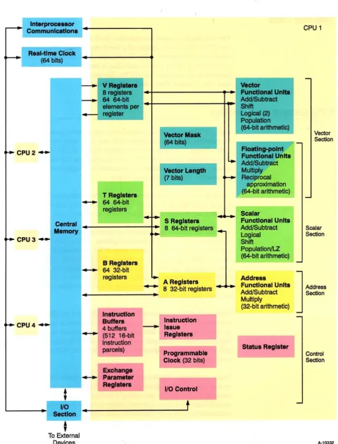
CPU Computation Section
Each CPU has an identical, independent computation section consisting of operating registers, functional units, and instruction issue control logic. Figure 2-1 shows the computation section of CPU 0 for a four-processor mainframe. The operating registers and functional units of each computation section are associated with three types of
processing: address, scalar, and vector.
Address processing operates on internal control information, such as loop counts, addresses, and indices. This processing uses address (A)
registers and dedicated integer arithmetic functional units.
Address information originates from central memory, from constant instruction values, or from control registers. Information in the A registers is distributed to various parts of the instruction issue control for use in controlling the scalar, vector, and I/O operations. The A registers can also supply operands to the add and multiply functional units. The units generate address and index information and return the result to the A registers. Address information can also be transmitted to central memory from the A registers.
Scalar and vector processing can also be performed on data. Scalar processing occurs sequentially and uses one operand or operand pair to produce a single result. Scalar processing is performed using scalar (S) registers, several functional units dedicated solely to scalar processing, and additional floating-point functional units shared with vector operations.
I
I
Interpr0C8ssor Communications~
I
Real-time Clock(64 bits)
!
1
-
VReglstera8 registers
-
64 64-bltelements per
---I register
~CPU2-T Registers
-
64 64-bitregisters
Central Memory
~CPU3-B Registers
-
64 32-bitregisters
..
Instruction Buffers
~CPU4- 4 buffers
...
(512 16-bit-t
r
VO1.
..
I
Sectionr
t
To External Devices
I
instruction parcels) Exchange Parameter Registers - ' Vector FunCtional Units Add/Subtract Shift logical (2)Population (64-bit arithmetic) Vector Mask
(64 bits)
Floatlng-polnt
~
1-t.,.. Functional Units Add/Subtract
Vector Length Multiply
f7
bits) ~ Reciprocalapproximation (64-bit arithmetic)
Scalar
1
-
.... 1 S Registers ' ... Functional Units~, 8 64-bit registers _ Add/Subtract
Logical Shift
Population/LZ (64-bit arithmetic)
-
-• A Reg... Add.... ]
... 8 32-b't g'sters...-4.... Functional Units
.. I re I Add/Subtract
Multiply (32-blt arithmetic)
-Instruction-
Issue Registers-
I
Status Register
l
I
ProgrammableClock (32 bits) J
-VO Control
t
-CPU 1
Vector Section Scalar Section Address Section Control Section
[image:24.609.62.543.57.687.2]A-10332
The main advantage of vector processing over scalar processing is that vector processing eliminates instruction start-up time for all but the first operand. Execution time for vector operations is short enough that vector processing is more efficient than scalar processing for vectors containing as few as two elements. Register-to-register vector instructions eliminate the problem of memory conflicts.
Data flow in a computation section is from central memory to registers and from registers to functional units. Results flow from functional units to registers and from registers to central memory or back to functional units. Data flows along either the scalar or vector path, depending on the instruction. An exception is that scalar registers can provide one
required operand for some vector instructions.
The computation section performs integer or floating-point arithmetic operations such as logical operations, indexing, population count, and leading-zero counts.
Integer, or fixed-point, operations are integer addition, integer
subtraction, and integer multiplication. Integer arithmetic is performed
in two's complement mode. No integer divide instruction is provided; the operation is accomplished through a software algorithm using floating-point hardware.
Floating-point instructions include addition, subtraction, multiplication, and reciprocal approximation. Floating-point quantities have signed magnitude representation. The reciprocal approximation instructions are used with a multiply instruction sequence to perform a floating-point divide operation.
The instruction set includes logical operations for AND, inclusive OR, exclusive OR, exclusive NOR, and a mask-controlled merge operation. Shift operations allow the manipulation of either 64-bit or 128-bit operands to produce 64-bit results. With the exception of address integer arithmetic, most operations are implemented in vector and scalar
instructions.
Index calculation is the integer product of a scalar instruction. Full indexing capability is possible throughout memory in either scalar or vector modes. The index can be positive or negative in either mode. Indexing allows matrix operations in vector mode to be performed on rows or on the diagonal, as well as allowing conventional column operations.
Registers
Address Registers
Each CPU has three primary and two intermediate sets of registers. The primary sets of registers are the address (A), scalar (S), and vector (V)
registers. These registers are considered primary because central memory and the functional units can access them via intermediate registers.
For the A and S registers, an intermediate level of registers exists. These registers are not accessible to the functional units, but act as a buffer for the primary registers. Block transfers of data from consecutive locations are possible between these registers and central memory so that the number of memory reference instructions required for scalar and address operands is greatly reduced. Data can then be moved from the
intermediate registers to the primary register when needed. The intermediate registers that support the A registers are referred to as intermediate address (B) registers. The intermediate registers that support S registers are referred to as intermediate scalar (T) registers.
Each CPU contains eight 32-bit A registers. The A registers serve a variety of applications, but are primarily used as address registers for memory references and as index registers. They also provide values for shift counts, loop control, and channel
110
operations and receive values of population count and leading zeros count. In address applications, A register 0 contains the base address for scalar and vector memory . references. In addition, the A registers provide an address increment for vector memory references.Each CPU contains 64 B registers; each register is 32 bits wide. The B registers are used as intermediate storage for the A registers. Data is transferred between B registers and central memory, and between A and B registers. Typically, B registers contain data to be referenced
Scalar Registers
Vector Registers
Functional Units
Each CPU contains eight S registers; each register is 64 bits wide. The S registers are the principal scalar registers for a CPU. Scalar registers serve as the source and destination for scalar arithmetic and logical instructions. Scalar registers can also provide an operand for some vector operations.
Each CPU contains 64 T registers; each register is 64 bits wide. The T registers are used as intermediate storage for the S registers. Data is transferred between T registers and central memory, and between T and S registers.
Each CPU contains eight vector (V) registers. Each V register consists of 64 elements; each element is 64 bits wide. The V registers serve as the source and destination for vector arithmetic and logical instructions. Successive elements from a V register are sent to a functional unit in successive CPs with a single instruction.
The effective length of a V register for any operation is controlled by the program-selectable vector length (VL) register. The VL register is a 7 -bit register that specifies the number of vector elements processed by vector instructions. The contents range from 08 through 1008.
The vector mask (VM) register allows for the logical selection of particular elements of a vector during merge and test instructions. The VM register has 64 bits, each corresponding to a word element in a V register. The high-order bit of the VM register corresponds to element 0 of the V register, while the low-order bit corresponds to element 63. Refer to "Vector Processing" in this section for more information on vector processing.
Instructions other than simple transmit or control operations are
Address Functional Units
Scalar Functional Units
Segmentation" and ''Functional Unit Independence" in this section for more information on segmentation, pipelining, and functional unit independence.
The functional units are described in four groups: address, scalar, vector, and floating-point. Each of the first three groups functions with one of the primary register types (A, S, and V) to support the address, scalar, and vector processing modes. The fourth group, floating-point, supports either scalar or vector operations and accepts operands from or delivers results to S or V registers. In addition, central memory can also act as a functional unit for vector operations.
Address functional units perform integer arithmetic on operands obtained from A registers and deliver the results to an A register (integer
arithmetic is explained later in this section). The following list describes the two address functional units.
•
•
The address add functional unit performs integer addition and subtraction; subtraction is performed by using two's complement arithmetic. Overflow is not detected.
The address multiply functional unit forms an integer product from two operands. No rounding is performed and overflow is not detected. The unit returns only the least significant bits of the product.
Scalar functional units perform operations on operands obtained from S registers and usually deliver the results to an S register (integer
arithmetic is explained later in this section). The exception is the population/parity/leading zero count functional unit, which delivers its result to an A register.
The scalar add, scalar shift, scalar logical, and scalar
population/parity/leading zero count functional units are used exclusively with scalar operations and are described here. Three additional
functional units are used for both scalar and vector operations. They are described in the following "Floating-point Functional Units" subsection. The following list describes the four scalar functional units.
Vector Functional Units
•
•
•
The scalar add functional unit performs integer addition and subtraction; subtraction is performed by using two's complement arithmetic. Overflow is not detected.
The scalar shift functional unit shifts the entire contents of an S register or shifts the contents of two concatenated S registers into a single resultant S register. Single shifts are end-off with zero fill, while double shifts can be circular fill. Shift counts are obtained from an A register or from the jk field of the instruction.
The scalar population/parity /leading zero count functional unit receives operands from an S register and delivers results to an A register. The population/parity functional unit counts the number of bits in an S register having a value of one and then, depending on the instruction issued, returns either a 7 -bit population value or a 1-bit population parity count value. For the leading zero function, it counts the number of 0 bits preceding a 1 bit in the operand from left to right.
Vector functional units perform operations on successive elements of one or two V registers, or on successive elements from a V register and a copy of an S register. The vector add and logical functional units require two operands, while the vector shift and population/parity functional units require only one operand. Results from a vector functional unit are delivered to a V register.
For operations using vector elements and a copy of a scalar register, the contents of the scalar register are transferred once to the functional unit and held there to be used as a constant. Successive operand pairs are transmitted each CP to a functional unit. The corresponding result emerges from the functional unit n CPs later, where n is the functional unit time and is constant for a given functional unit.
There are four general-purpose memory ports for each CPU: port A through port D, of which port D is used for I/O channels and as a fetch operations unit. The VL register determines the number of operands or operand pairs to be processed by a functional unit. Refer to "Special Features of the CPU" in this section for more information on vector processing, chaining, and other special vector processing features. The CRAY Y-MP EL CPU features four sets of vector functional unit execution units (BUs), EU 0 through EU 3. Each EU contains a copy of every vector functional unit plus floating-point add and multiply
EU has one data path to registers. As a result, a CPU can simultaneously perform four vector add or four vector multiply operations, or any combination thereof.
The functional units described in this subsection are used exclusively with vector operations. Three functional units are used with both vector and scalar operations, and are described in the following "Floating-point Functional Units" subsection. The following list describes the four vector functional units.
• The vector add functional unit performs integer addition and subtraction for a vector operation and delivers the results to elements of a V register. Subtraction is performed by using two's complement arithmetic. Overflow is not detected.
• The vector shift functional unit shifts the entire contents of a V register element or the value formed from two consecutive elements of a V register. Shift counts are obtained from an A register. All shifts are end-off with zero fill.
• The full vector logical functional unit performs a bit-by-bit manipulation of specified quantities for specific instructions. The full vector logical functional unit also performs vector register merge, compressed index, and logical operations associated with the vector mask instructions.
• The vector population/parity functional unit counts the number of bits set in each element of the source V register; the result is the population count. This population count can be an odd or an even number, as shown by its low-order bit. The vector population count instruction delivers the total population count to elements of the destination V register. The vector population count parity instruction delivers only the low-order bit of the count to the destination V register. This bit can be used to determine even or odd parity.
Floating-point Functional Units
floating-point functional unit is used for a vector operation, the general description of vector functional units given in the individual subsection applies.
The following list describes the three floating-point functional units.
•
•
The floating-point add functional unit performs addition or
subtraction of operands in floating-point format. The final result is normalized even when operands are unnormalized. The
floating-point add functional unit detects overflow and underflow conditions; only overflow conditions are flagged. (Refer to "Normalized Floating-point Numbers" in this section for more information on normalized numbers.)
The floating-point multiply functional unit performs full- and half-precision multiplication of operands in floating-point format. The half-precision product is rounded; the full-precision product can be rounded or not rounded. This functional unit also generates a 32-bit integer product.
Input operands are assumed to be normalized. The floating-point multiply functional unit delivers a normalized result only if both input operands are normalized.
Out-of-range exponents are detected. If both operands have zero exponents, the result is considered an integer product, is not normalized, and is not considered to be out of range.
• The reciprocal approximation functional unit calculates the
approximate reciprocal of an operand in floating-point format. The input operand is assumed to be normalized. The high-order bit of the coefficient is not tested, but is assumed to be a 1. Out-of-range exponents are detected. Reciprocal approximation operations are used in conjunction with multiply operations to perform an add operation.
Functional Unit Operations
Functional units in a CPU perform logical operations, integer arithmetic, and floating-point arithmetic. Both types of arithmetic are performed using two's complement arithmetic. The following subsections explain and define the logical operations, the integer arithmetic, and the
Logical Operations
Integer Arithmetic
Scalar and vector logical units perform bit-by-bit manipulation of 64-bit quantities. Instructions are provided for forming logical products, sums, differences, equivalences, and merges.
A logical product is the AND function shown below. Operand 1: 1010
Operand 2: 1 1 0 0 Result: 1 0 0 0
A logical sum is the inclusive OR function shown below. Operand 1: 1010
Operand 2: 1 1 0 0 Result : 1 1 1 0
A logical difference is the exclusive OR function shown below. Operand 1: 1010
Operand 2: 1 1 0 0 Result: 0 1 1 0
A logical equivalence is the exclusive NOR function shown below. Operand 1: 1010
Operand 2: 1 1 0 0 Result: 1 0 0 1
The merge uses two vperands and a mask to produce results as shown below. The bits of operand 1 are transmitted when the mask bit is a 1.
The bits of operand 2 are transmitted when the mask bit is a O.
Operand 1: 1 0 1 0 1 0 1 0 Operand 2: 1 1 0 0 1 1 0 0 Mask: 1 1 1 1 0 0 0 0 Result: 1 0 1 0 1 1 0 0
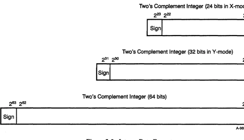
Two's Complement Integer (24 bits in X-mode)
Two's Complement Integer (32 bits in V-mode)
Two's Complement Integer (64 bits)
[image:33.617.129.537.73.307.2]A-9887
Figure 2-2. Integer Data Formats
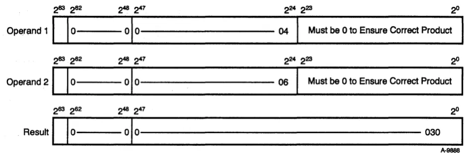
Multiplication of two scalar (64-bit) integer operands is done using the floating-point multiply instruction and one of two mUltiplication methods. The method used depends on the magnitude of the operands and the number of bits available to contain the product. The following paragraphs explain the 24-bit integer multiply operation and the method used for operands greater than 24 bits in length.
The floating-point multiply functional unit recognizes the condition in which both operands have zero exponents as a special case; it is treated as an integer multiply operation, and a complete multiply is performed with no truncation as long as the total number of bits in the two operands does not exceed 48 bit positions. To multiply two integers together, set each operand's exponent equal to zero and place each 24-bit integer value in bit positions 247 through 224 of the operand's coefficient field. To ensure accuracy, the least significant 24 bits must be O.
When the floating-point multiply functional unit has performed the operation, it returns the high-order 48 bits of the product as the result coefficient and leaves the exponent field as O. The result is a 48-bit quantity in bit positions 247 through 2°; no normalization shift of the result is performed.
OPE!rand 1 I 10- - - -
+---
04I
Must be 0 to Ensure Correct ProductI
Operand 2 0 - - - -
---06
Must be 0 to Ensure Correct Product [image:34.613.70.538.69.223.2]~~HI lo---olo---~o~
Figure 2-3. 24-bit Integer Multiply Performed in Floating-point Multiply Functional Unit
A-9888
The second multiplication method is used when the operands are greater than 24 bits in length; multiplication is done by software forming multiple partial products and then shifting and adding the partial products.
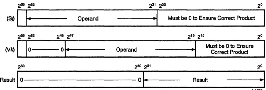
A second integer multiplication operation performs a 32-bit
multiplication operation on the Sj and the Vk operands and puts the result in the Vi register. The operands must be left-shifted before the operation begins. The Sj operand must be left-shifted 3110 places, leaving the operand in bit positions 262 through 231; bit positions 230 through 2° must be equal to 0 to ensure accuracy (refer to Figure 2-4). The Vk operand must be shifted left 1610 places, leaving the operand in bit positions 247 through 216; bit positions 215 through 2° must be equal to 0 to ensure accuracy. The result of the multiply is right justified into positions 231 through 2°, while positions 232 through 263 are filled with zeros.
Operand
---1
•
.,.1 Must be 0 to Ensure Correct Product(VI<)
1 1
0- - 0 - Operand ---.,~IJ
Must be 0 to Ensure Correct ProductResult
1
0 - - - 0 ....1·1---
Result·1
Floating-point Arithmetic
[image:35.615.101.549.70.221.2]Floating-point Data Format
Figure 2-4. 32-bit Integer Multiply Performed in Floating-point Multiply Functional Unit
A-9B89
Floating-point arithmetic is used by the scalar and vector instructions. The following subsections explain the floating-point data format,
exponent ranges, normalized floating-point numbers, floating-point range errors, the floating-point addition, multiplication, and division
algorithms, and double-precision numbers.
Floating-point numbers are represented in a standard format throughout the CPU; this format is shown in Figure 2-5. The format has three different fields: coefficient sign, exponent, and coefficient.
Coefficient Sign
262
Coefficient Sign
Binary Point
~1~7
Exponent Coefficient
[image:36.613.76.544.65.705.2]A-9890
Figure 2-5. Floating-point Data Format
The coefficient is a 48-bit signed fraction; the sign of the coefficient is
located in bit position 263• Because the coefficient is in sign-magnitude
format, it is not complemented for negative values. A normalized floating-point number has a 1 in the 247 bit position, while an
unnormalized floating-point number has a 0 in this bit position
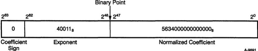
(normalized numbers are discussed in more detail later in this section). Figure 2-6 and the following steps show the relation between the bias, exponent, and coefficient.
To convert a floating-point number to its decimal equivalent:
1. Subtract the bias from the exponent to get the integer value of the exponent:
400118 - 400008
118
=
9102. Multiply the normalized coefficient by the power of 2 indicated in the exponent to get the result:
0.56348 X 29
=
563.408=
371.510A zero value or an underflow result is not biased and is represented as a word of all O's. A negative 0 is not generated by any floating-point functional unit, except when one operand going into the floating-point multiply or floating-point add functional unit has a value of negative O.
Binary Point
400118 56340000000000008
Exponent Normalized Coefficient
[image:36.613.119.534.598.681.2]A-9891
Exponent Ranges
4 200008
The exponent portion of the floating-point format is represented as a biased integer in bits 262 through 248. The bias that is added to the exponents is 400008, which represents an exponent of 2°. Figure 2-7 shows the biased and unbiased exponent ranges.
In terms of decimal values, the floating-point format of the system allows the accurate expression of numbers to about 15 decimal digits in the approximate decimal range of 10-2466 through 10+2466•
Biased Exponent Range
Negative Range Positive Range
400008
I
Unbiased Exponent Range A-9892
Figure 2-7. Biased and Unbiased Exponent Ranges
Normalized Floating-point Numbers
A nonzero floating-point number is normalized if the most significant bit of the coefficient, bit 247, is nonzero. This condition implies that the
coefficient has been shifted as far left as possible and that the exponent has been adjusted accordingly; therefore, a normalized floating-point number has no leading O's in its coefficient. The exception is a normalized floating-point 0, which is all O's.
When a floating-point number is created by inserting an exponent of 400608 and a 48-bit integer word into the coefficient, the result should be normalized before being used in a floating-point operation.
Normalization is accomplished by adding the unnormalized floating-point operand to O.
Floating-point Range Errors
263 262
Overflow
I
0 Sign263 262
underflowl 0
1
0
Sign
The floating-point add functional unit does not require normalized numbers to get correct results. The floating-point add functional unit does, however, automatically normalize all its results; unnormalized floating-point numbers may be routed through this functional unit to take advantage of this process.
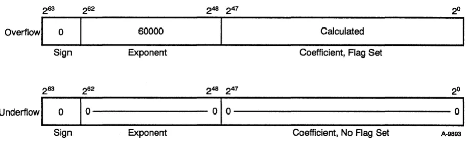
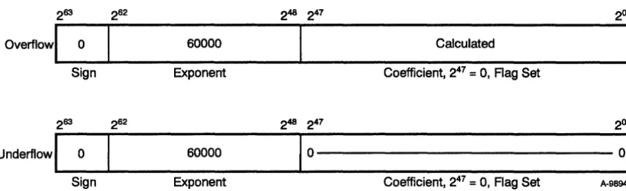
To make sure the limits of the functional units will not be exceeded, a range check is made on the exponent of each floating-point number for overflow and underflow conditions. In the floating-point add and multiply functional units, bits 261 and 262 are checked; if both bits are equal to 1, the exponent is equal to or greater than 600008 and an overflow condition is detected. The calculated coefficient is reported, but the exponent is set to 600008 and the floating-point error flag is set (refer to Figure 2-8).
When an overflow condition is detected, an interrupt occurs only if the interrupt-on floating-point error (IFP) bit is set in the mode register and the system is not in monitor mode. The IFP flag can be set or cleared by a user mode program.
To check for an underflow condition in the floating-point add and multiply functional units, bits 261 and 262 are checked; if both are equal to 0, then the exponent is less than or equal to 177778 and an underflow condition is detected. No flag is set, but the exponent and coefficient are both set to O's (refer to Figure 2-8).
248 247 2°
60000 Calculated
Exponent Coefficient, Flag Set
248 247 2°
01
001
[image:38.613.84.540.454.593.2]Exponent Coefficient, No Flag Set A·9893
Figure 2-8. Floating-point Add and Multiply Range Errors
In the reciprocal approximation functional unit, the exponent is
263 262
Overflow
I
0 Sign263 262
Underflow
I
0 Signcondition. In this case, the calculated coefficient is reported, but bit 247 is set to 0, the exponent is set to 600008, and the floating-point error flag is set (refer to Figure 2-9).
248 247 2°
60000 Calculated
Exponent Coefficient, 247
=
0, Rag Set248 247 2°
60000
1
0
01
[image:39.617.91.544.137.275.2]Exponent Coefficient, 247
=
0, Flag Set A-9894Figure 2-9. Floating-point Reciprocal Approximation Range Errors
Again, because the reciprocal approximation operation complements and adds 2 to a floating-point number, the exponent must be less than or equal to 200018 for an underflow condition to occur. 1bis underflow condition then causes an overflow condition in the original exponent. In
this case, the calculated coefficient is reported, but bit 247 is set to 0, the exponent is set to 600008, and the floating-point error flag is set (refer to Figure 2-9).
Floating-point Addition Algorithm
Floating-point addition or subtraction is performed in a 49-bit register to allow for a sum that might carry into an additional bit position. The algorithm performs three operations: equalizing exponents, adding coefficients, and normalizing the results.
To equalize the exponents, the larger of the two exponents is retained. The coefficient of the smaller exponent is right-shifted by the difference of the two exponents, or until both exponents are equal. Bits shifted out of the register are lost; no round-up operation occurs. Because the coefficient is only 48 bits in length, any shift beyond 48 bits causes the smaller coefficient to become O's.
The following list shows how the operation is determined.
• If the sign bits are equal and an add instruction is issued, an add operation is performed.
• If the sign bits are not equal and an add instruction is issued, a subtraction operation is performed.
• If the sign bits are equal and a subtract instruction is issued, a subtract operation is performed.
• If the sign bits are not equal and a subtract instruction is issued, an add operation is performed.
The last operation performed normalizes the results. To normalize the result, the coefficient is left-shifted by the number of leading D's (the coefficient is normalized when bit 247 is a 1). The exponent must also decrement accordingly. If a carry across the binary point occurs during an addition operation, the coefficient is right-shifted by 1 and the
exponent increases by 1. If a carry across the binary point occurs during a subtraction operation, an end-around carry occurs.
The normalization feature of the floating-point add functional unit can be used to normalize any floating-point number. Adding an unnormalized number to a zero operand will normalize the number.
A range check is performed on the result of all additions; refer to "Floating-point Range Errors" in this section for more information on how the result is checked.
Floating-point Multiplication Algorithm
The floating-point multiply functional unit receives two floating-point operands from either an S or V register. The signs of the two operands are combined using an exclusive OR operation, the exponents are added together, and the two 48-bit coefficients are multiplied together. If the coefficients are both normalized, multiplying them together produces a full product of either 95 or 96 bits. A 96-bit product is normalized as generated, while a 95-bit product requires a left-shift of one to generate the final coefficient. If the shift is performed, the final exponent is reduced by 1 to reflect the shift.
Because the result register (an S or V register) can hold only 48 bits in
Floating-point Division Algorithm
The functional unit truncates part of the low-order bits of the 96-bit product. To adjust for this truncation, a constant is unconditionally added above the truncation. The average value of this truncation is 9.25 X 2-56, which is determined by adding all carries produced by all
possible combinations that could be truncated and dividing the sum by the number of possible combinations. Nine carries are inserted at bit position 2-56 to compensate for the truncated bits.
The effect of the truncation without compensation is at most a result coefficient 1 smaller than expected. With compensation, the results range from 1 too large to 1 too small in the 2-48 bit position, with
approximately 99% of the values having zero deviation from what would have been generated had a full 96-bit product been present. The
multiplication is commutative; that is, A X B = B
x
A.Rounding is optional, while truncation compensation is not. The
rounding method used adds a constant so that it is 50% high (0.25 x 2-48; high) 38% of the time and 25% low (0.125
x
2-48; low) 62% of the time, resulting in a near-zero average rounding error. In a full-precision rounded multiply, 2 round bits are entered into the summation at bit positions 2-50 and 2-51 and allowed to propagate.For a half-precision multiply, round bits are entered into the summation at bit positions 2-32 and 2-31. A carry resulting from this entry is allowed to propagate up and the 29 most significant bits of the normalized result are transmitted back.
The variations due to this truncation and rounding are in one of the following ranges:
--0.23 X 2-48 to +0.57 X 2-48 or
-8.17 X 10⁻¹⁶ to +20.25 X 10⁻¹⁶
With a full 96-bit product and rounding equal to one-half the least significant bit, the following variation is expected.
--0.5 X 2-48 to +0.5 X 2-48
Finding the quotient of two floating-point numbers involves two steps. For example, to find the quotient of
NB,
first, the B operand is sent through the reciprocal approximation functional unit to obtain itsreciprocal,
lIB.
Then, this result, along with the A operand is sent to the floating-point multiply functional unit to obtain the product of AxlIB.
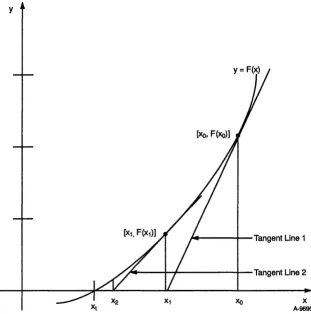
The reciprocal approximation functional unit uses an application of Newton's method for approximating the real root of an arbitrary equation, F(x)
=
0, to find reciprocals.To find the reciprocal, the equation, F(x)
=
1/x - B, must be solved. To do this, a number, A, must be found so that F(A)=
1/A - B= o.
That is, the number A is the root of the equation 1/x - B= o.
The method requires an initial approximation (or guess, which is shown as Xo in Figure 2-10) sufficiently close to the true root (which is shown as Xt inFigure 2-10). Xo is then used to obtain a better approximation; this is done by drawing a tangent line (line 1 in Figure 2-10) to the graph of y
=
F(x) at the point [Xo, F(Xo)]. The intercept of this tangent line becomes the second approximation, Xl. This process is repeated, usingtangent line 2 to obtain X2, and so on.
The following iteration equation is derived from this process:
In the equation, x(x + 1) is the next iteration, Xi is the current iteration, and
B is the divisor. Each XCi + 1) is a better approximation than Xi to the true value, Xt. The exact answer is generally not obtained at once because the
y
J4----+-Tangent Line 1
·~--+--1'---+-Tangent Line 2
[image:43.613.228.539.74.387.2]X A-9895
Figure 2-10. Newton's Method for Approximating Roots
The CPU uses this approximation technique based on Newton's method. A hardware lookup table provides an initial guess, Xo, to start the process. The following iterations are then calculated.
Iteration Operation Description
The first approximation is done in the reciprocal approximation functional unit and is accurate to 8 bits.
The second approximation is done in the reciprocal
4 The fourth approximation is done in the floating-point multiply functional unit to calculate the correction term. The reciprocal approximation functional unit calculates the first three iterations, while the the floating-point multiply functional unit calculates the fourth iteration. The fourth iteration uses a special instruction within the floating-point mUltiply functional unit to calculate the correction term. This iteration is used to increase accuracy of the reciprocal approximation functional unit's answer to full precision (the floating-point multiply functional unit can provide both full- and half-precision results). A fifth iteration should not be done.
The following example shows how the floating-point mUltiply functional unit is used to provide a full-precision result, solving the equation S1/S2.
1
2
3
4
Operation S3
=
1/S2S4
=
[2-(S3*
S2)]S5
=
S4*
S3S6
=
S5*
S1Performed By
Reciprocal approximation functional unit
Floating-point multiply functional unit
Floating-point multiply functional unit using
full-precision; S5 now equals 1/S2 to 48-bit accuracy Floating-point multiply functional unit using full-precision rounded
The reciprocal approximation in Step 1 is correct to 30 bits. By Step 3, it is accurate to 48 bits. This iteration answer is applied as an operand in a full-precision rounded multiply operation (Step 4) to obtain a quotient accurate to 48 bits. Additional iterations may produce erroneous results. Where 29 bits of accuracy are sufficient, the reciprocal approximation instruction is used with the half-precision multiply to produce a
half-precision quotient in only two operations, as shown in the following example.
Operation
1 S3 = 1/S2
Performed by
Double-precision Numbers
Operation
2 S6
=
S1*
S3Performed by
Floating-point mUltiply
functional unit in half-precision The 19 low-order bits of the half-precision results are returned as D's with a rounding applied to the low-order bit of the 29-bit result.
The reciprocal iteration is designed for use once with each half-precision reciprocal generated. If the iteration performed by the floating-point multiply functional unit results in an exact reciprocal or if an exact reciprocal is generated by some other method, performing another iteration results in an incorrect final reciprocal.
The following process is another method of computing division: Operation
1 S3
=
1/S22 S5
=
S1*
S33 S4
=
[2 - (S3*
S2)]4 S6
=
S4*
S5Performed by
Reciprocal approximation functional unit
Floating-point multiply functional unit
Floating-point multiply functional unit
Floating-point multiply functional unit
In this method the correction to reach a full-precision reciprocal is done after the number is multiplied by the half-precision reciprocal, rather than before the multiplication.
The coefficient of the reciprocal produced by this alternative method can be different by as much as 2 x 2-48 from the first method described for generating full-precision reciprocals. This difference can occur because one method can round up as much as twice, while the other method may not round at all. One round can occur while the correction is generated and the second round can occur when producing the final quotient. Therefore, if the reciprocals are to be compared, use the same method each time the reciprocals are generated.
CPU Control Section
Exchange Mechanism
Exchange Sequence
Exchange Package
The control section of the CPU issues program instructions. Before program instructions can issue, exchange and instruction fetch sequences must occur. The following subsections describe the exchange
mechanism (which includes defining both the exchange package and exchange sequence), and the instruction fetch and instruction issue sequences.
Each CPU uses an exchange mechanism for switching instruction execution from program to program. This exchange mechanism uses a CPU operation referred to as an exchange sequence and blocks of program parameters known as exchange packages.
An exchange sequence occurs before a program can begin running. An exchange sequence performs two simultaneous functions. First, program parameters for the next program are loaded from central memory into registers in the CPU. Second, parameters from the previous program are read from the registers and stored back into central memory.
The program parameters are held in an exchange package, which is described in the following subsections. The contents of the A and S registers are automatically saved in the exchange package; the contents of the B, T, V, VM, shared address (SB), shared scalar (ST), and semaphore (SM) registers must be saved by software.
Exchange sequences may be initiated by a deadstart sequence or program exit, voluntarily by the software, or automatically upon occurrence of an interrupt condition. All instructions previously issued are allowed to complete before the exchange sequence begins. An instruction fetch always follows an exchange sequence. Refer to "Instruction Fetch" in this section for more information on this sequence.
Processor Number Field
Memory Error Data Fields
Program Address Register Field
The contents of the processor number (PN) field in the exchange package indicates which CPU performed the exchange sequence. This value is not stored initially in the exchange package before program execution; it
is a constant inserted into the exchange package after the program ran and exchanged out.
Memory error data, consisting of six fields of information, appears in the exchange package only if one of two conditions is met. The first
condition is that the interrupt-on-correctable memory error bit is set and a correctable memory error is encountered. The second condition is that the interrupt-on-uncorrectable memory error bit is set and an
uncorrectable memory error is detected. Memory error data fields are described below.
•
•
•
•
•
•
The syndrome field defines a SECDED error on a memory read or I/O channel.
The read address bank field defines the bank where a memory read error occurred.
The read error type field defines the type of memory or I/O error encountered; the error can be either correctable or uncorrectable.
The port field defines the port where a memory read or I/O error occurred; these bits are used with the read mode bits to identify the operation in error.
The read address chip select field identifies the chip on which a memory read error occurred.
The read mode field determines the type of read mode in progress when a memory data error occurred; these bits are used with the port bits to identify the operation in error.
Address Base and Limit Fields
Four registers in the exchange package define a program's data range and instruction range anywhere in memory and allocate specific amounts of memory to each range. This memory allocation technique has two benefits. First, all programs are relocatable. When a program is written, the programmer does not need to know where in memory the instruction and data fields will be located. Second, each program can have its memory access restricted to certain parts of memory. A program can be halted if it tries to run an instruction outside of its allowed instruction range or if it tries to read or write data outside of its allowed data range. This is especially important where more than one program occupies memory at the same time; programs can be prevented from executing instructions or operating on data that belongs to other programs. The four registers are described in the following list.
•
•
•
•
The instruction base address (IBA) register holds the base address of the user's instruction range. It determines where in memory an instruction fetch is made. This is done by adding the contents of the P register to the contents of the rnA register. The sum equals the absolute memory address for the fetch.
The instruction limit address (ILA) register holds the upper limit address of the user's instruction range. It determines the highest absolute address that can be accessed during an instruction fetch sequence. If this absolute address exceeds the limit, a program range error flag is set, which generates an interrupt.
The data base address (DBA) register holds the base address of the user's data range. It determines where in memory a program's data field is located. This is done by adding the memory address generated by the instruction to the contents of the DBA register. The sum equals the absolute address for any memory read or write operation.
The data limit address (DLA) register holds the upper limit address of the user's data range. It determines the highest absolute memory address that a program can use for reading or writing data. If this absolute address exceeds the limit, the memory reference is aborted. The operand range error flag is set, which generates an interrupt if the interrupt-on-operand range error bit is set.
Exchange Address Register Field
Vector Length Register Field
Cluster Number Register Field
Flag Register Field
exchange package must begin on a 16-word boundary. The 12-bit limit requires that the absolute address be in the lower 4,096 (100008) words of memory. When an execution interval terminates, the exchange sequence exchanges the contents of the registers with the contents of the exchange package at the beginning address (XA) in memory.
The vector length (VL) register specifies the length of all vector
operations performed by vector instructions and the number of elements held by the V registers. The value in the VL register can be changed by software while a program is running.
The cluster number (CLN) register determines which set of SB, ST, and SM registers the CPU can access. If the CLN register is 0, the CPU does not have access to any SB, ST, or SM register. The contents of the CLN register in all CPUs are also used to determine the condition necessary for a deadlock interrupt.
The flag (F) register contains several flags, which when set, interrupt program execution by initiating an exchange sequence. The contents of the F register are stored along with the rest of the exchange package during the exchange sequence. The monitor program can then analyze the flags for the cause of the interrupt. Before the monitor program exchanges back, it must clear the flags in the F register area of the exchange package. If any bit remains set, another exchange occurs immediately.
The F register contains the following flags:
•
•
•
•
Interrupt-from-internal CPU (ICP) flag; set when another CPU issues instruction 0014j1.
Deadlock (DL) flag; set when all CPUs in a cluster are holding issue on a test and set instruction.
Programmable clock interrupt (PCI) flag; set when the programmable clock reaches a count of O.
Mode Register Field
•
•
•
•
•
•
•
Floating-point error (FPE) flag; set when a floating-point range error occurs in any of the floating-point functional units and the interrupt-on-floating-point error (IFP) bit in the M register is set. Operand range error (ORE) flag; set when a data reference is made outside the boundaries of the DBA and DLA registers and the interrupt-on-operand range error bit is set.
Program range error (PRE) flag; set when an instruction fetch is made outside the boundaries of the rnA and ILA registers. Memory error (ME) flag; set when a correctable or uncorrectable memory error occurs and the corresponding interrupt-on-memory error (IME) bit in the M register is set.
I/O interrupt (101) flag; set when a 6-Mbyte/s channel or a lOOO-Mbyte/s channel completes a transfer.
Error exit (EEX) flag; if not in monitor mode or if the
interrupt-in-monitor mode bit is set, this flag is set by an error exit instruction.
Normal exit (NEX) flag; if not in monitor mode, this flag is set by a normal exit instruction.
The mode (M) register contains user-selectable bits that dictate the execution of the program. It also contains 2 status bits (program state and floating-point error status) that are set by software and hardware, respectively, during an exchange sequence. The M register contains the following bits:
•
•
•
•
Program state (PS) bit; this bit is set by the operating system to show whether a CPU, concurrently processing a program with another CPU, is the master or slave in a multitasking situation.
Floating-point error status (FPS) bit; when set, a floating-point error occurred regardless of the state of the
interrupt-on-floating-point error bit.
Bidirectional memory (BDM) bit; when set, block reads and writes can operate concurrently.
Vector Not Used Field
Waiting for Semaphore Field
Concurrent Block Write
•
•
•
•
•
•
•
Interrupt-on-floating-point error (IFP) bit; when set, this bit enables interrupts on floating-point errors.
Interrupt-on-uncorrectable memory error (ruM) bit; when set, this bit enables interrupts on uncorrectable memory data errors and on register parity bits.
Interrupt-on-correctable memory error (ICM) bit; when set, this bit enables interrupts on correctable memory data errors.
Extended addressing mode (EAM) bit; when set, this bit indicates that 32-bit (Y -mode) addressing takes place. When it is not set, this bit indicates that 24-bit (X-mode) addressing takes place. Selected for external interrupts (SEI) bit; this bit designates the CPU with priority for I/O interrupts.
Interrupt monitor mode (IMM) bit; when set, this bit enables all interrupts in monitor mode except the programmable clock interrupt, MCU interrupt, interrupt-on-internal CPU, and I/O interrupt.
Monitor mode (MM) bit; when set, this bit inhibits all interrupts except memory errors, normal exit, and error exit.
The state of the vector not used (VNU) bit in the exchange package indicates whether vector register instructions were issued during the execution intervals. If no vector register instructions were issued, the bit is set. H one or more of the vector register instructions were issued, the bit is not set.
The state of the waiting for semaphore (WS) bit indicates that the CPU exchanged when a test and set instruction was holding in the current instruction parcel (CIP) register.