Single-Switch, Wide Voltage-Gain Range, Boost DC-DC
Converter for Fuel Cell Vehicles
Yun Zhang, Member, IEEE, Lei Zhou, Mark Sumner, SeniorMember, IEEE, and Ping Wang
Abstract—In order to match voltages between the fuel cell stacks and the DC link bus of fuel cell vehicles, a single-switch Boost DC-DC converter with diode-capacitor modules is proposed in this paper. The capacitors are charged in parallel and discharged in series. The wide voltage-gain range can be obtained by using a simple structure. In addition, the basic operating principles, the extended stages, the fault tolerant operation, and steady-state characteristics of the converter are analyzed and presented in this paper, and the small-signal model is also derived. A 400V, 1.6kW experimental prototype is developed, and the wide voltage-gain range (3.3~8) is demonstrated with a maximum efficiency at 97.25%. The experimental results validate the effectiveness and feasibility of the proposed converter and its suitability as a power interface for fuel cell vehicles.
Index Terms—Boost DC-DC converter; Fault tolerant operation; Fuel cell vehicles; Low voltage stress; Single-switch; Wide voltage-gain range.
I. INTRODUCTION
Challenges associated with CO2 reduction and
depleting fossil fuel resources [1]-[4] together with the increasing penetration of renewable resources [5]-[8] has focused research into the electrification of transport including hybrid and full electric vehicles (EVs) [9]-[12]. Fuel cell vehicles have the advantages of high energy conversion efficiency and zero emissions together with a higher range than battery vehicles [13]-[15]. However, fuel cells output a relatively low voltage and high current and they cannot be used directly for electric vehicles which require a high DC bus voltage (e.g. 400V) [16]. In
Copyright (c) 2015 IEEE. Personal use of this material is permitted. However, permission to use this material for any other purposes must be obtained from the IEEE by sending a request to [email protected].
order to match the low voltage of fuel cells with the high DC bus voltage required for EVs, a high voltage-gain Boost DC-DC converter is needed to act as the power interface between the fuel cell stacks and the DC bus. In addition, a battery pack can be connected to the DC bus by a bidirectional DC-DC converter, resulting in a high efficiency powertrain [17]-[18]. Moreover, the output voltage of fuel cells drops with the increasing output power [19]. Therefore, the Boost DC-DC converter for fuel vehicles needs to operate with a wide voltage-gain range.
The conventional Boost DC-DC converter has an ideal voltage-gain of 1/(1-d), where d is the duty cycle of the active power switch. However, the high voltage-gain is limited by the effects of parasitic resistance and extreme duty cycles, and the voltage stress seen by all the semiconductors used is as high as the output voltage [20]-[22]. Even though the three-level Boost DC-DC converter can reduce the voltage stress to half of the output voltage, the ideal voltage-gain is still 1/(1-d) [23]. In addition, a complicated control strategy is needed for the flying-capacitor voltage to balance the voltage stress
seen by all the semiconductors [24]. The
grounds pulsates at the switching frequency. This condition will limit its applications due to the additional electromagnetic interference created.
In addition to widening the voltage-gain range of the Boost DC-DC converter for fuel cell vehicles and reducing its conduction and switching losses, the dv/dt of the potential difference between the input and output grounds of the converter should be zero (i.e. a common ground) or very small. In order to improve the performance over the previously discussed approaches, a single-switch wide voltage-gain range Boost DC-DC converter is proposed in this paper. The voltage stress across all the semiconductors is half of the output voltage, the voltage-gain is 2/(1-d), which is double that of the conventional Boost DC-DC converter, and the variation of the potential difference between the input and output grounds is very small. In Section II, the topology of the proposed converter is introduced, and the operating principle is analyzed in Section III. In Section IV, small-signal model for the proposed converter is developed together with its steady-state analysis and the fault tolerant operation. In Section V, an experimental prototype is developed, and the experimental results are presented to validate the proposed converter.
II. TOPOLOGY
The development of the proposed topology is shown in Fig.1. The diode-capacitor branches with the common inductor are in Fig.1(a). D2-C1 and D1-C2 are two
diode-capacitor modules; they are charged in parallel by the input voltage source Uin and the inductor L. In
Fig.1(b), D3-C3 is another diode-capacitor module, and Q-C1 is reconstructed as a switched-capacitor module
from the diode-capacitor module D2-C1. The energy
stored in C1 can then be transferred to C3 through the
active power switch Q and the diode D3. Therefore, the
total voltage of the output capacitors C2 and C3 in series is
double that of the conventional Boost DC-DC converter. Therefore, a single-switch wide voltage-gain Boost DC-DC converter is created as shown in Fig.1(c).
From Fig.1(c), it can be seen that the proposed topology is comprised of one inductor, one active power switch and three diode-capacitor modules with C1=C2=C3.
iL is the inductor current of L, iQ is the current through Q,
and iD1, iD2 and iD3 are the currents flowing in D1, D2 and D3, respectively. UQ is the blocking voltage across Q, UD1, UD2 and UD3 are the voltage stresses across D1, D2 and D3,
respectively. UC1, UC2 and UC3 are the voltages across C1, C2 and C3. Uo is the output voltage, and Io is the load
current.
(a)
(b)
(c)
Fig.1 Development of the proposed topology. (a) Diode-capacitor branches with the common inductor. (b) Diode/switch-capacitor branches with the energy transferring. (c) Single-switch wide voltage-gain Boost DC-DC converter.
III. OPERATING PRINCIPLES FOR THE PROPOSED
CIRCUIT
operating waveforms of the proposed topology are shown in Fig.3.
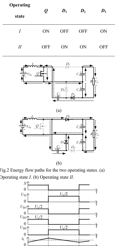
TABLE. I Turn-on and turn-off states of the corresponding semiconductors under two operating states.
Operating
state
Q D1 D2 D3
I ON OFF OFF ON
II OFF ON ON OFF
(a)
[image:3.595.47.286.142.646.2](b)
[image:3.595.318.550.650.755.2]Fig.2 Energy flow paths for the two operating states. (a) Operating state I. (b) Operating state II.
Fig.3 Operating waveforms for the proposed topology. Operating state I (t0-t1): when the active power switch Q
is turned on, the inductor L is charged from Uin, C3 is
charged by C1 through Q and D3, and the load resistor R is
supplied by C2 as shown in Fig.2(a). Therefore, D1 and D2
are turned off and see blocking voltages of UC2 and UC3,
respectively. The inductor current iL rises linearly, and
the output voltage Uo is the combined voltages of C2 and C3, i.e. Uo=UC2+UC3.
Operating state II (t1-t2): when Q is turned off, Uin and
the inductor L in series discharge into the two
diode-capacitor modules in parallel, i.e. C1 and C2 are
charged in parallel. In addition, the load resistor R is supplied by Uin, L, and C3 in series as shown in Fig.2(b).
Therefore, the voltage stress across Q is UC2, and D3 is
turned off with a blocking voltage of UC3. The inductor
current iL falls linearly, and the output voltage Uo is the
total voltage of Uin, UL and UC3, i.e. Uo=UC2+UC3.
IV. SMALL-SIGNALMODEL,STEADY-STATE
ANALYSIS AND FAULT TOLERANT OPERATION
A. Small-signal model
Assuming that C1=C2=C3=C, and the inductance and
capacitance of the inductor and capacitors are large
enough. The average model and small-signal model can
be obtained by using the state-space averaging method. The duty cycle of the active power switch Q is d.uin(t), uo(t) and d(t) are the input variable, the output variable
and the control variable, respectively. iL(t), uC1(t), uC2(t)
and uC3(t) are the state variables. According to Fig.2(a), C1 and C3 are connected in parallel while the active power
switch Q and diode D3 are turned on, which means the
voltages across C1 and C3 are equal. So, there is an invalid
state variable in uC1(t) and uC3(t). Similarly, as shown in
Fig.2(b), the voltages across C1 and C2 are equal, which
means there is also an invalid state variable in uC1(t) and uC2(t). By considering the series resistance r of capacitor
C1, the coupling between the capacitors can be removed
to avoid the invalid state variables.
When Q is turned on, the converter is operated in operating state I, and the state space average model can
be obtained as follows:
[ ]
L
L C1
C1
in C2
C2
C3 C3
o L C1
d ( )
0 0 0 0
d 1
1 1 ( )
d ( ) 0 0
( )
d 0
( )
1 1
( )
d ( ) 0 0
0
d ( )
0
1 1
d ( ) 0
d
( ) 0 0 1 1 ( ) ( ) i t
t
i t
u t L
Cr Cr u t
t
u t u t
u t
CR CR
t u t
R r u t
Cr CR CRr
t
u t i t u t
−
= +
− −
+
− −
= [ ]T
C2( ) C3( )
u t u t
When Q is turned off, the converter is operated in operating state II, and the state space average model can
be written as:
[ ] L L C1 C1 in C2 C2 C3 C3 o L
d ( ) 1
0 0 0
d 1
( )
1 1
d ( )
0 0
( )
d 0
( )
1 1 1 ( )
d ( )
0
d ( )
0
1 1
d ( )
0 0 d
( ) 0 0 1 1 ( ) i t t L i t u t L u t Cr Cr t u t
R r u t
u t
C Cr CRr CR
t u t
u t
CR CR
t
u t i t u
− − = + + − − − −
= [ ]T
C1( )t uC2( )t uC3( )t
(2)
Combining (1) and (2), the average model of the converter can be obtained as:
L L C1 C1 C2 C2 C3 C3
d ( ) 1 ( )
0 0 0
d
( ) 1 1 ( ) ( ) d ( )
0 ( )
d
1 ( ) 1 ( ) 1 ( ) 1 1 ( ) d ( )
( )
d ( )
( ) 1 1 ( ) d ( )
0 ( )
d
i t d t
t L
i t
d t d t
u t
u t
Cr Cr Cr
t
d t d t d t u t
u t
C Cr Cr CR CR
t u t
d t d t
u t
Cr CR CR Cr
t − − − − = − − − − + − − − + [ ][ ] in T
o L C1 C2 C3
1 0 ( ) 0 0
( ) 0 0 1 1 ( ) ( ) ( ) ( )
L u t
u t i t u t u t u t
+ = (3)
The state variables, the input variable, the output variable and the control variable can be described by introducing small-signal disturbance variables as:
L L L
C1 C1 C1
C2 C 2 C2
C3 C 3 C3
in in n
o o o
ˆ ( )= + ( ) ˆ ( ) ( ) ˆ ( ) ( ) ˆ ( ) ( ) ˆ ( ) ( ) ˆ ( ) ( ) ˆ ( ) ( ) i i t I i t
u t U u t
u t U u t
u t U u t
u t U u t
u t U u t d t D d t
= + = + = + = + = + = + (4)
where IL, UC1, UC2, UC3, Uin, Uo and D are the steady state
components, i tˆ ( )L , uˆ ( )C 1 t , uˆ ( )C2 t , uˆ ( )C3 t , u tˆ ( )in and d tˆ ( )
are the small-signal disturbance variables. Combining (3) and (4), the small-signal model of the converter can be written as L L C1 C1 C2 C2 C3 C3 ˆ 1
d ( )
0 0 0
d
ˆ ( ) 1 1
ˆ d ( )
0 ˆ ( )
d
1 1 1 1 1 ˆ
ˆ ( )
d ( ) ( )
d ˆ ( )
1 1
ˆ
d ( ) 0 ( )
d 1 0 0 0 D i t L t i t D D u t u t
Cr Cr Cr
t
D D D u t
u t
C Cr Cr CR CR
t u t
D D
u t
Cr CR CR Cr
t L − − − − = − − − − + − − − + + [ ] L C1 in C2 C3 T
o L C1 C2 C3
1
0 0 0
1 1 0 0
ˆ
ˆ ( ) ( )
1 1 1 0
1 1
0 0
ˆ
ˆ( ) 0 0 1 1 ( ) ˆ ( ) ˆ ( ) ˆ ( )
L I U Cr Cr
u t d t
U
C Cr Cr U
Cr Cr
u t i t u t u t u t
− + − − − = (5)
B. Steady-state analysis
When the converter is operated in steady-state, the values of the small-signal disturbance variables are 0. Simplifying (3) and (4), IL, UC1, UC2, UC3, and Uo can be
obtained as (6):
o L in C1 C2 in in C3 in o 2 (1 )
[ (1 ) 2 ]
(1 )[ (1 ) ]
1 1
[ ( 1) ]
( 1)[ (1 ) ]
2 (1 )
DU I
RD D r
U RD D r Dr
U
D RD D r
U U
D
U RD D r
U
D RD D r
RDU U
RD D r
= − + − + − = − − + = − − + = − − + = − + (6)
Assuming that the resistance r is 0, simplifying (6), the (7) can be obtained as:
L o
C1 C2 C3 in
o in 2 1 1 1 2 1 I I D
U U U U
D U U D = − = = = − = − (7)
According to (7) and Fig.2, the voltage stress across all the semiconductors can be described as:
o Q D1 C2
o D2 C1 o D3 C3 2 2 2 U
U U U
U U U U U U = = = = = = = (8)
Based on (7) and (8), all the capacitor voltages are half of the output voltage (these are the voltage stresses across
all the semiconductors). However, the voltage-gain M of
the proposed topology is double that of the conventional Boost DC-DC converter (9):
2 1
M d =
− (9)
Then, the duty cycle can be calculated as
2 1
d M
= − (10)
The current stress on all the semiconductors can be
deduced from the ampere-second equations for C1–C3,
Fig.2, and (7) as:
Q o
D1 D2 o
D3 o
2 1
( )
1 1 1 1
I I
d d
I I I
d
I I
d
= +
−
= =
−
=
(11)
According to (7) and (11), it can be seen that the current stress IQ on Q is larger than the inductor current IL.
However, IQ moves closer to IL as the voltage-gain
increases. In addition, the current stress on D1 and D2 is
half of the inductor current, and the current stress on D3 is
(1-d)/d times larger than the inductor current.
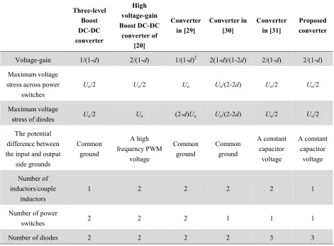
The comparisons among the three-level Boost DC-DC converter, the high voltage-gain Boost DC-DC converter in [28], the converters in [29]-[31] and the proposed Boost DC-DC converter are shown in TABLE. II. From
the comparison in TABLE. II, it can be seen that the voltage-gain of the proposed converter is higher than that of the three-level Boost DC-DC converter, while the voltage stress and the number of the active power switches and inductors are lower than those of the high voltage-gain Boost DC-DC converter in [28].
According to TABLE. II, the converters in [29] and [30] also have a higher voltage-gain. But the proposed converter can achieve an additional lower voltage stress across the power semiconductors. The single switch hybrid DC-DC converter in [31] can obtain the same voltage-gain and the same voltage stress across the semiconductors, as well as a constant capacitor voltage between the input and output grounds. However, it needs one more inductor and one more capacitor, which may
improve the volume, and reduce the efficiency.
TABLE. II Comparisons among the topologies.
Three-level Boost DC-DC converter
High voltage-gain Boost DC-DC
converter of [20]
Converter in [29]
Converter in [30]
Converter in [31]
Proposed converter
Voltage-gain 1/(1-d) 2/(1-d) 1/(1-d)2 2(1-d)/(1-2d) 2/(1-d) 2/(1-d)
Maximum voltage stress across power
switches
Uo/2 Uo/2 Uo Uo/(2-2d) Uo/2 Uo/2
Maximum voltage
stress of diodes Uo/2 Uo (2-d)Uo Uo/(2-2d) Uo/2 Uo/2
The potential difference between the input and output
side grounds
Common ground
A high frequency PWM
voltage
Common ground
Common ground
A constant capacitor
voltage
A constant capacitor
voltage
Number of inductors/couple
inductors
1 2 2 2 2 1
Number of power
switches 2 2 2 1 1 1
[image:5.595.63.534.392.739.2]According to the previously analyzed, the proposed converter has these advantages: (a) a high voltage-gain which is double that of the conventional Boost DC-DC converter. (b) a low voltage stress across the power semiconductors which is half of the output voltage. So it is easier (and cheaper) to choose the power semiconductors for the converter, and the switching losses can also be reduced due to the lower on-state resistance. (c) a constant capacitor voltage across the input and output side grounds, which means the variation of the potential difference is very small.
However, there are still some disadvantages for the proposed converter: (a) the current stress on the power switch is high a little bit, it may cause additional power losses. (b) the input current ripple is not low enough, comparing with that of the conventional interleaved Boost converter, due to employing a single inductor and only one active power switch.
C. Stability analysis
1. Stability analysis of the proposed converter
When Uo=400V, d=0.75, L=234µH, C1=C2=C3=470µF,
R=100Ω, and r=30mΩ, according to (5), the
input-to-output transfer function Gio(s) and the
control-to-output transfer function Gdo(s) can be obtained
from the time domain to the complex frequency domain as:
in
o io
ˆ in ( ) 0
9 2 4
15 4 10 3 6 2 4
o do
ˆ ( ) 0
10 3 5 2 15 4 10 3
ˆ ( ) ( )
ˆ ( )
4.97 10 6.17 10 9.38
2.19 10 3.1 10 6.2 10 3.3 10 1.17
ˆ ( ) ( )
ˆ( )
1.49 10 1.75 10 0.16 1875 2.19 10 3.1 10 6.2 10
d s u s u s G s u s s s
s s s s
u s
G s
d s
s s s
s s = − − − − − − = − − − − = × + × + = × + × + × + × + = − × − × − + =
× + × + × 6 2 4
3.3 10 1.17
s s − − + × + (12)
The PI voltage controller is adopted in the proposed converter, and the voltage loop control scheme of the proposed converter is shown in Fig.4.
ref
ˆ ( )
u s d sˆ( ) u sˆ ( )o
in
ˆ ( )
u s
Fig.4 Voltage loop control scheme of the proposed converter.
E(s) is the image function of e(t) in the complex frequency domain. The transfer function GPI(s) of the PI
voltage controller, the transfer function GPWM(s) of the
pulse-width modulator (PWM), and the feedback transfer function H(s) can be obtained as
PI
PWM
0.0008 ( ) 0.0001
( ) 1 ( ) 1 G s s G s H s = + = = (13)
Assuming that uˆ ( )in s =0, according to Fig.4, the
closed-loop transfer function can be obtained by combining (12) and (13) as follows:
5 4
5 4 2 5
( )
6.81( 1.06 10 )( 1.77 10 )( 6677)( 8) ( 1.18 10 )( 2.4 10 )( 1.1)( 38.64 2.2 10 ) G s
s s s s
s s s s s
=
− + × + × − +
+ × + × + + + ×
(14)
According to (14), all the real parts for the poles of the closed-loop transfer function are less than 0. Therefore, the closed-loop system of the proposed converter with the PI voltage controller can operate stably.
Assuming that uˆ ( )ref s =0, according to Fig.4, (12) and
(13), the steady-state error ess(t) can be described as
ss
0
in 0
PI PWM do
2 in 0
( ) lim ( ) lim ( ) ( )
ˆ
lim ( )
1 ( ) ( ) ( ) ( ) ˆ
0.78 lim ( )
t s
s
s
e t e t sE s
H s
s u s
G s G s G s H s s u s
→∞ → → → = = = − + = − (15)
According to (15), to make the steady-state error ess(t)=0,
the disturbance variable of the input voltage uˆ ( )in t needs
to satisfy (16) as follows:
2 in 0 ˆ
lim ( ) 0
s→ s u s = (16)
where uˆ ( )in s is the image function of uˆ ( )in t . (16) can be
simplified as (17) by applying the final-value theorem
in
ˆ
d ( )
lim 0
d
t
u t t
→∞ = (17)
If the voltage variation of the input voltage uˆ ( )in t
satisfies (16) or (17), the closed-loop system of the proposed converter can operate stably.
2. Influences of the input inductor and output
capacitors
It should be noticed that (10) is deduced under ideal
conditions. The parasitic parameters and the
losses which can reduce the voltage-gain of the converter. Therefore, in order to obtain the real voltage-gain of the proposed converter, the duty cycle d will be a bit higher than the calculated value from (10). The equivalent circuit of the proposed converter considering the equivalent series resistors of the input inductor L, the output capacitors C2 and C3 is shown in Fig.5, where R is
the load resistor, rLis the equivalent series resistance of L, rC2 and rC3 are the equivalent series resistances of C2 and C3.
Fig.5 The equivalent circuit of the proposed converter. According to Fig.5, the following equations can be obtained by applying the ampere-second balance principle on C1-C3
D3 D 2
o D1 o
o D 3 o
L D1 D2
(1 )
(1 ) ( )
(1 ) ( )
d I d I
d I d I I
d I d I I
I I I
× = − ×
× = − × −
− × = × −
= +
(18)
where ID1, ID2 and ID3 are the average currents of diodes D1, D2 and D3 in the ON state, respectively. Simplifying
(18), IL, ID1, ID2 and ID3 can be obtained as
L o
D1 o
D2 o
D3 o
2 1
1 1
1 1
1
I I
d
I I
d
I I
d
I I
d
=
−
=
−
=
−
=
(19)
The input power Pin and the power losses P2 of C2 and C3
can be calculated respectively as
in in L
2 2 2 2 2
2 L L [ o (D1 o) ]C2 [ o ( D 3 o) ]C3
P U I
P I r I I I r I I I r
=
= + + − + + −
(20)
Combining (19) and (20), the output voltage Uo can be
obtained as:
in 2 o
o
2 2
in 4 3 2
1 2 3 C3 C3
2 (1 )
4
P P U
I
Rd d
U A d A d A d r d r
− =
− =
− + − +
(21)
where
1 C2 C3 2 C2 C3 3 L C2 C3
2 2
2 6 2
4 7
A r r R
A r r R
A r r r R
= + +
= + +
= + + +
(22)
According to (21), the real voltage-gain of the proposed converter considering the equivalent series resistors of the input inductor L, the output capacitors C2 and C3 can
be described as:
2 2 4 3 2
1 2 3 C3 C3
2 (1 )
4
Rd d M
A d A d A d r d r −
=
− + − + (23)
Therefore, when the proposed converter operates with the voltage-gain range 3.3~8, the duty cycle range will be a bit higher than 0.4~0.75.
Influences of the series resistances of the input inductor and the output capacitors on the proposed converter can be equivalent as a disturbance variable γ(t). The value of
γ(t) is a constant one that is less than 0, and it will reduce the duty cycle of the converter. Assuming that γ(t)=c, when the disturbance of the input voltage is 0, the voltage loop control scheme of the proposed converter with the disturbance γ(t) is shown in Fig.6, where γ(s) is the image function of γ(t) in the complex frequency domain.
ref
ˆ ( )
u s d sˆ( ) u sˆ ( )o
Fig.6 The voltage loop control scheme with the disturbance γ(t). Assuming that uˆ ( )ref s =0, according to Fig.6, (12), and
(13), the steady-state error ess(t) can be obtained as:
ss
0 do 0
PI PWM do 2
0
( ) lim ( ) lim ( )
( ) ( )
lim ( )
1 ( ) ( ) ( ) ( )
1249.9 lim ( )
t s
s
s
e t e t sE s G s H s
s s
G s G s G s H s s s
γ
γ
→∞ →
→
→
= =
= − + = −
(24)
When γ(t)=c (i.e. γ(s)=c/s), according to (24), the steady-state error is ess(t)=0, which means the proposed
under the control of the closed-loop system will be higher than the calculated value by (10).
D. The DC-DC Boost converter with extended stages The proposed converter can be extended with more stages. The topology of the extended DC-DC Boost converter is shown in Fig.7. As shown in Fig.7, the topology consists of (2n-1) capacitors and (2n-1) diodes. A high voltage-gain can be obtained by extending the number of capacitors and diodes. Fig.8 shows the on/off states of the power semiconductors in the extended DC-DC Boost converter with "n" stages. When the active power switch Q is turned on, the on/off states of the diodes are shown in Fig.8 (a). Fig.8 (b) shows the on/off states of the diodes while the active power switch Q is turned off.
Fig.7 The topology of the DC-DC Boost converter with extended stages.
The output voltage Uo of the extended DC-DC Boost
converter with "n" stages is:
o C in
1 n
U nU U
D
= =
− (25)
The voltage stress across each power semiconductor is equal
o
Q D C in
1 1 U
U U U U
n D
= = = =
− (26)
where UQ is the voltage stress across the active power
switch Q, and UD is the voltage stress across each diode.
E. Fault tolerant operation
In order to improve the reliability of the proposed converter, a fault tolerant operation under a power semiconductor failure is required. The fault tolerant operation scheme for the proposed converter is based on
that in [32]. Then, the fault tolerant operation circuit of the proposed converter is shown in Fig.9.
(a)
(b)
Fig.8 The on/off states of power semiconductors in the DC-DC Boost converter with extended stages. (a) Q is turned on. (b) Q
is turned off.
Fig.9 The fault tolerant operation circuit of the proposed converter.
In terms of Fig.1 (c) and Fig.9, the fuses F, F1, F2 and F3
and the auxiliary power switches Qoc, Qoc1, Qoc2 and Qoc3
are required for the fault tolerant operation. When the converter operates in the normal state, Qoc, Qoc1, Qoc2 and Qoc3 are turned off. When a failure (i.e. a short circuit or
tolerant condition, by employing the corresponding fuse and the auxiliary power switch.
1. Fault detection and identification
When Q operates in a normal condition, the waveform
of UQ is shown in Fig.3. The failure of Q can be detected
by the signal of UQ and the gate signal S. When S=1 and UQ=Uo/2, it means the open-circuit fault occurs with Q.
When S=0 and UQ=0, it indicates the short-circuit fault
happens with Q. Therefore, the signal "sgnQ" can be
obtained as follows:
Q Q
Q
0, sgn
1, U U
δ δ >
=
<
(27)
where δ is a small value between 0 and Uo/2.
The signal "errQ" is defined as
Q Q
err = ⊕S sgn (28)
When there is no semiconductor failure, signals S and sgnQ have the same value, and the signal errQ is equal to 0,
according to (28). When a failure happens, the value of sgnQ is different from that of S, thus the value of errQ is
equal to 1. It should be noted that the value of errQ will be
0 when signals S and sgnQ have the same value again.
However, the sampling period and the parasitic
parameters in the converter cannot be neglected. When Q
operates in a normal condition, there is a time delay between signals S and sgnQ. During this delay, errQ will
be equal to 1 even there is no switch failure in the converter. Therefore, the strategy of the fault detection and identification for the main power switch Q can be obtained in Fig.10.
By means of Fig.10, when the converter operates in a steady state, "errQ=0" means there is no switch failure.
When the value of the signal errQ becomes 1, the counter
is activated and its output signal nc is increased. The
signal errQ is also observed at the same time. If nc>N
(where the value of N should be predefined), the duration of "errQ=1" is longer than the observation time NTsam,
where Tsam is the sampling period. Then it is concluded
that there is a failure with Q (NTsam must be longer than
the time delay caused by the sampling period and the parasitic parameters). If the gate signal S is equal to 1 while nc>N, it can be concluded that the open-circuit fault
occurs with Q. Then the values of the signals for the
open-circuit fault (OCF) and the short-circuit fault (SCF)
become OCF=1 and SCF=0. If the gate signal S is equal
to 0 while nc>N, the short-circuit fault will be detected
with Q, then the values of the signals become OCF=0 and
SCF=1.
Fig.10 The strategy of fault detection and identification for the main power switch Q.
It should be noticed that only when the duration of "errQ=1" is longer than NTsam, the fault tolerant operation
would work. When an open-circuit fault happens with Q,
the duration of "errQ=1" is always shorter than dTs. When
a short-circuit fault happens with Q, the duration of "errQ=1" is always shorter than (1-d)Ts. Therefore, if the
switching period Ts is close to NTsam, the fault tolerant
operation cannot detect the failures with Q. In order to make the fault tolerant operation work properly, Tsam must
be much shorter than Ts.
2. Remedial actions
The control method of the power switch Qoc for the fault
tolerant operation is shown in Fig.11.
Fig.11 The control method of the power switch Qoc for the fault
tolerant operation.
SQoc is the gate signal of Qoc. According to Fig.9 and
Fig.11, when an open-circuit fault occurs with Q, the
signal OCF will be set to 1. Then Q will be replaced by
the power switch Qoc, and the gate signal SQoc is the same
be isolated by the fuse F from the circuit (i.e. the branch related with Q is in the open circuit). Then, the power switch Qoc will replace the power switch Q, while the
signal SCF is set to 1. In addition, SQoc is also the same as S.
The fault tolerant operations of the diodes D1, D2 and D3
are similar to that of the power switch Q. It should be noted that the gate signals of Qoc1 and Qoc2 need to be
complementary to S, while the gate signal of Qoc3 should
be the same as S. The fault tolerant operation method for the diodes D2 and D3 can also be used for the diodes in the
DC-DC Boost converter with extended stages.
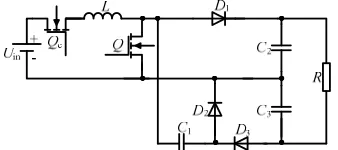
The proposed converter with the protection for the capacitor failures is shown in Fig.12. The additional power switch QC is used to protect the converter when the
[image:10.595.85.254.338.413.2]capacitor fails.
Fig.12 The proposed converter with the protection of the capacitors.
When the converter operates in a steady-state under the
voltage loop control, the output voltage Uo is
substantially equal to the reference voltage Uref. Uo will
decrease to 0.5Uref or 0 when the capacitor failures
happen, which are almost related to the short-circuit faults. Therefore, the signal "sgnC" can be defined as
follows:
o ref C
o ref
0, sgn
1,
U kU U kU
<
=
>
(29)
where k is a constant value that satisfies 0.5<k<1. When sgnC=1, Uo is equal to Uref, there is no capacitor failure in
the converter. When a capacitor failure occurs, "sgnC"
will be equal to 0. The signal "m(t)" can be obtained as follows:
0 0
1, ( )
0,
t t m t
t t <
=
>
(30)
where t0 is the transient time that the converter operates
from the starting to the steady-state. The gate signal of QC
can be obtained by (29) and (30) as follows:
C sgnC ( )
S = +m t (31)
where “+” represents the logical relationship “OR”. According to (31), during the transient time t0, SC is
equal to 1, QC is turned on, the converter operates in a
normal state. When a capacitor failure occurs, SC is equal
to 0, then QC will be turned off to protect the converter.
V. EXPERIMENTAL RESULTS AND ANALYSIS
A 1.6kW prototype has been developed, in which a TMS320F28335 DSP is adopted as the controller to form a voltage control loop. An IXYS-IXTK102N30P MOSFET and IXYS-DPG60C300HB Schottky diodes have been selected as the active power switches and diodes, respectively. The switching frequency is
fs=20kHz, the value of the inductor is L=234µH, and the
capacitors are C1=C2=C3=470µF. The input voltage
changes continuously between Uin=50V~120V, and the
output voltage is controlled constant at Uo=400V; the
load resistor is R=100Ω. The experimental prototype is developed, as shown in Fig. 13.
The voltage stress across all the semiconductors and the inductor current for Uin=50V and Uo=400V are shown
in Fig.14. It can be seen in Fig.14(a) that the duty cycle of the active power switch Q is about d=0.76, (as opposed to approximately d=0.9 for the three-level Boost DC-DC converter), when the voltage-gain M is 8. In addition, the blocking voltage UQ of Q is 200V (i.e. half the output
voltage). The average inductor current is 35A when the output power is 1.6kW. At the same time, the voltage stress across D1-D3 is 200V (again half the output
voltage), as shown in Fig.14(b, c). Therefore, the single-switch Boost DC-DC converter can perform with a high voltage-gain and a low device voltage stress if a proper duty cycle is used.
The voltages UC2 and UC3 across C2 and C3 (the output
capacitors in series) for Uin=50V and Uo=400V are shown
in Fig.15. Because these two capacitors are charged and discharged with the same duty cycle, UC2 and UC3 are
both at constant 200V. In addition, the potential difference between the input and output grounds is the voltage across C3, i.e. constant at 200V with a very small
ripple, i.e. a very small dv/dt.
UQ (100V/div)
iL (10A/div)
t(10µs/div)
0.76
d≈
(a)
UD2 (100V/div)
UD1 (100V/div)
t(10µs/div)
(b)
UD2 (100V/div)
UD3(100V/div)
t(10µs/div)
(c)
Fig.14 Voltage stress across all semiconductors and inductor current when Uin=50V and Uo=400V. (a) Voltage stress across Q and inductor current. (b) Voltage stresses across D1 and D2. (c)
Voltage stresses across D2 and D3.
With the control of the voltage loop, the output voltage
Uo can be still controlled at constant 400V, even though
the input voltage Uin changes from 120V to 50V
continuously over 16 seconds, as shown in Fig.16(a). Therefore, the proposed converter can operate well with a wide voltage-gain range, e.g. from 3.3 to 8. The inductor current iL rises from 14A to 35A following to the falling
input voltage, as shown in Fig.16(b).
UC2(100V/div)
UC3(100V/div)
t(10µs/div)
Fig.15 Voltages across C2 and C3 under Uin=50V and Uo=400V.
Uo(100V/div) Uin(20V/div)
400V
120V
50V
t(2s/div)
(a)
120V
50V
t(2s/div)
iL (10A/div) Uin(20V/div)
(b)
Fig.16 Output voltage and dynamic inductor current when Uin
at constant 400V with the control of the voltage loop. It
can be seen that iin changes from 6.5A to 10A over 8ms
with the load step-change from 200Ω to 130Ω, and it recovers from 10A to 6.5A over 8 ms with the load step-change from 130Ω to 200Ω.
For the operation of the proposed converter with a wide input-voltage range, the conversion efficiencies related to the variable input voltages (e.g. 50V, 60V,···, 110V, 120V) and the different output powers (e.g. 800W, 1200W, 1600W) are measured using a power analyzer (YOKOGAWA/WT3000) as shown in Fig.18, when the switching frequency fs is 20kHz. When the converter
outputs 1200W, it has its maximum efficiency 97.25%
while the input voltage is Uin=120V. And the minimum
efficiency is 90.53% when the input voltage is changed to
Uin=50V. Therefore, the efficiency falls with the
increased voltage-gain, due to the increased losses caused by the increased inductor current.
.
Uo(100V/div)
iin(10A/div)
t(40ms/div) Load step-change
from 200 to 130Ω Ω
Load step-change from 130 to 200Ω Ω
Fig.17 Output voltage and input current with load step-change between 130Ω and 200Ω.
50 60 70 80 90 100 110 120
90 91 92 93 94 95 96 97 98
800W 1200W 1600W
E
ff
ic
ie
n
c
y
/%
Uin(V)
fs=20kHz
Fig.18 Relationship among efficiency, variable input voltages and different output powers when fs=20kHz.
VI. CONCLUSION
A single-switch Boost DC-DC converter with a wide voltage-gain range is proposed in this paper. It employs one active power switch and less number of inductors and capacitors to operate over a wide voltage-gain range with the appropriate duty cycle. In addition, the voltage stress across all the semiconductors is as low as 1/n of the output voltage, and the potential difference between the input and the output grounds is constant. It is suitable for the power interface of fuel cell vehicles.
REFERENCES
[1] U. K. Madawala, P. Schweizer, and V. V. Haerri, “Living and mobility—A novel multipurpose in-house grid interface with plug-in hy-brid Blue Angle,” ICSET'08, pp. 531-536, Sep. 2008.
[2] B. Zeng, J. Zhang, X. Yang, J. Wang, J. Dong, and Y. Zhang, “Integrated planning for transition to low-carbon distribution system with renewable energy generation and demand response,” IEEE Trans. on Power Syst., vol. 29, no. 3, pp. 1153–1165, May 2014.
[3] P. Muthukrishnan, and R. Dhanasekaran, “A high step-up converter with a voltage multiplier & coupled inductor module for photovoltaic system,” ICACCT'14, pp. 1041-1045, May 2014.
[4] H. Rudnick, “Evolution of energy: global developments and challenges,” IEEE Power Energy Mag., vol. 10, no.3, pp. 12-19, May 2012.
[5] Q. Zhai, S. Alberts, H. Cao, S. Zhao, and C. Yuan, “Strength analysis of international feed-in tariff promotion of clean energy applications for greenhouse gas emission mitigation,” IEEE International Symposium on Sustainable Systems and Technology, pp. 1-6, 2010. [6] J. Mao, L. Gu, A. Wu, G. Wu, X. Zhang, and D. Chen,
“Back-stepping control for vertical axis wind power generation system maximum power point tracking based on extended state observer,” CCC'16, pp. 8649-8653, Jul. 2016.
[7] C. Nguyen, and H. Lee, “A novel dual-battery energy storage system for wind power applications,” IEEE Trans. Ind. Electron., vol. 63, no. 10, pp. 6136-6147, Oct. 2016. [8] A. Nagarajan, and R. Ayyanar, “Design and strategy for the
Trans. Sustainable Energy, vol. 6, no. 3, pp. 1085-1092, Jul. 2015.
[9] T. Nonaka, and M. Nakano, “Study of popularization policy of clean energy vehicles using life cycle assessment,” ICISS'10, pp. 1-6, Jul. 2010.
[10]J. Jin, X. Chen, L. Wen, S. Wang, and Y. Xin, “Cryogenic power conversion for SMES application in a liquid hydrogen powered fuel cell electric vehicle,” IEEE Trans. on Appl. Superconductivity, vol. 25, no. 1, Feb. 2015. [11]V. Ivanov, D. Savitski, and B. Shyrokau, “A survey of
traction control and antilock braking systems of full electric vehicles with individually controlled electric motors,”
IEEE Trans. Veh. Technol., vol. 64, no. 9, pp. 3878-3896, Sep. 2015.
[12]M. Ahmadi, E. Galvan, E. Adib, and H. Farzanehfard, “New fully soft switched bi-directional converter for hybrid electric vehicles: analysis and control,” IECON'10, pp. 2340-2345, Nov. 2010.
[13]Y. Wu, and H. Gao, “Optimization of fuel cell and supercapacitor for fuel-cell electric vehicles,” IEEE Trans. Veh. Technol., vol. 55, no. 6, pp. 1748-1755, Nov. 2006. [14]U. R. Prasanna, X. Pan, A. K. Rathore, and K. Rajashekara,
“Propulsion system architecture and power conditioning topologies for fuel cell vehicles,” IEEE Trans. Ind. Appl., vol. 51, no. 1, Jan./Feb. 2015.
[15]Y. Zhang, Y. Mou, and Y. Yang, “An energy management study on hybrid power of electric vehicle based on aluminum air fuel cell,” IEEE Trans. Appl. Supercond.,vol. 26, no. 7, Oct. 2016.
[16]H. Chiu, and L. Lin, “A bidirectional DC-DC converter for fuel cell electric vehicle driving system,” IEEE Trans. Power Electron., vol. 21, no. 4, pp. 950-958, Jul. 2006. [17]A. A. Fardoun, E. H. Ismail, A. J. Sabzali, and M. A.
Al-Saffar, “Bidirectional converter for high-efficiency fuel cell powertrain”, J. Power Sources, vol. 249, pp. 470-482, Mar. 2014.
[18]M. Ahmadi, M. R. Mohammadi, E. Adib, and H. Farzanehfard, “Family of non-isolated zero current transition bi-directional converters with one auxiliary switch,” IET Power Electron., vol. 5, no. 2, pp. 158-165, 2012.
[19]J. Xiao, X. Zhang, S. Wen, and D. Wang, “DC-DC converter based on real-time PWM control for a fuel cell system,” ICAMS'14, pp. 561-566, Aug. 2014.
[20]O. Abutbul, A. Gherlitz, Y. Berkovich, and A. Ioinovici, “Step-up switching-mode converter with high voltage gain
using a switched-capacitor circuit,” IEEE Trans. on Circuits and Syst. I, vol. 50, no. 8, pp. 1098-1102, Aug. 2003.
[21]Q. Zhao, F. Tao, F. C. Lee, P. Xu, and J. Wei, “A simple and effective to alleviate the rectifier reverse-recovery problem in continuous-current mode boost converter”,
IEEE Trans. Power Electron., vol. 16, no. 5, pp. 649-658, Sep. 2001.
[22]C. Pan, and C. Lai, “A high efficiency high step-up converter with low switch voltage stress for fuel cell system applications,” IEEE Trans. Ind. Electron., vol.57, no. 6, pp. 1998-2006, Jun. 2010.
[23]G. Lefevre, and S. Mollov, “A soft-switched asymmetric flying capacitor Boost converter with synchronous rectification,” IEEE Trans. Power Electron., vol. 31, no. 3, pp. 2200-2212, Mar. 2016.
[24]K. Jin, X. Ruan, M. Yang, and M. Xu, “A hybrid fuel cell power system,” IEEE Trans. Ind. Electron., vol. 56, no. 4, pp. 1212–1222, Apr. 2009.
[25]B. Axelrod, Y. Berkovich, and A. Ioinovici, “Switched-capacitor/switched-inductor structures for getting transformerless hybrid DC–DC PWM converters,”
IEEE Trans. on Circuits and Syst. I, vol. 55, no. 2, pp. 687-696, Mar. 2008.
[26]G. R. Walker, and P. C. Sernia, “Cascaded DC-DC converter connection of photovoltaic modules,” IEEE Trans. Power Electron., vol. 19, no. 4, pp. 1130-1139, Jul. 2004.
[27]R. J. K. Prasana, S. Ramprasath, and N. Vijayasarathi, “Design and analysis of hybrid DC-DC boost converter in continuous conduction mode,” ICCPCT'16, pp. 1-5, 2016. [28]L. Yang, T. Liang, and J. Chen, “Transformerless DC-DC converters with high step-up voltage gain,” IEEE Trans. Ind. Electron., vol. 56, no. 8, pp. 3144-3152, Aug. 2009. [29]H. Ardi, A. Ajami, F. Kardan, and S. N. Avilagh, “Analysis
and implementation of a nonisolated bidirectional DC-DC converter with high voltage gain,” IEEE Trans. Ind. Electron., vol. 63, no. 8, pp. 4878-4888, Aug. 2016. [30]H. Shen, B. Zhang, D. Qiu, and L. Zhou, “A common
grounded Z-source DC-DC converter with high voltage gain,” IEEE Trans. Ind. Electron., vol. 63, no. 5, pp. 2925-2935, May 2016.
[32]E. Jamshidpour, P. Poure, E. Gholipour, and S. Saadate, “Single-switch DC–DC converter with fault-tolerant capability under open- and short-circuit switch failures,”
IEEE Trans. Power Electron., vol. 30, no. 5, pp. 2703-2712, Mar. 2015.
Yun Zhang (M’13) was born in Jiangsu, China, in 1980. He received the B.S. and M.S. degrees in electrical engineering from the Harbin University of Science and Technology, Harbin, China, in 2003 and 2006, respectively, and the Ph.D. degree in electrical engineering from the Harbin Institute of Technology, Harbin, China, in 2010.
In 2010, he joined the Tianjin University, Tianjin, China, as a Lecturer in the School of Electrical and Information Engineering, where he is currently an Associate Professor. From December 2016 to December 2017, he was an academic visitor with the Power Electronics, Machines and Control (PEMC) Group at the University of Nottingham, England, U.K.. His current research interests include topologies, modulation, and control strategies of power converters for electric vehicles and microgrids.
Dr. Zhang is an Associate Editor of the JOURNAL OF POWER
ELECTRONICS.
Lei Zhou was born in Ningxia, China. He received his B.S. degree in Electrical Engineering from the Tianjin University, Tianjin, China, in 2015. He started pursing his M.S. degree in Electrical Engineering from Tianjin University, Tianjin, China, in 2015. His current research interests include DC-DC converters, modeling and analysis of DC-DC converters.
Mark Sumner (SM’05) received the B.Eng. degree in electrical and electronic engineering from Leeds University, Leeds, U.K., in 1986, and the Ph.D. degree in induction motor drives from the University of Nottingham, Nottingham, U.K., in 1992.
He was with Rolls Royce, Ltd., Ansty, U.K. He was a Research Assistant with the University of Nottingham, where he became a Lecturer in October 1992, and is currently a Professor of electrical energy systems. His research interests include control of power electronic systems including sensorless motor drives, diagnostics and prognostics for drive
systems, power electronics for enhanced power quality, and novel power system fault location strategies.