ISSN Print: 2327-6045
DOI: 10.4236/msce.2018.67002 Jul. 4, 2018 8 Journal of Materials Science and Chemical Engineering
Feasibility Study to Evaluate Lattice-Space
Changing of a Step-Graded SiGe/Si (110) Using
STEM Moiré
Junji Yamanaka
1, Mai Shirakura
1, Chiaya Yamamoto
1, Kei Sato
1, Takane Yamada
1,
Kosuke O. Hara
1, Keisuke Arimoto
1, Kiyokazu Nakagawa
1, Akimitsu Ishizuka
2, Kazuo Ishizuka
21University of Yamanashi, Takeda, Kofu, Japan
2HREM Research Inc., Matsukazedai, Higashimastuyama, Japan
Abstract
A moiré between crystal lattice planes and scanning electron beam-lines formed in a scanning transmission electron microscope includes the informa-tion of the lattice spacing. We apply these phenomena to a composiinforma-tionally graded SiGe thin film deposited onto a Si substrate by molecular beam epitaxy method. The results of the experiments and image analysis show the potential of this technique to analyze a slight change of the lattice spacing according to a compositional change.
Keywords
STEM Moiré, SiGe, Scanning Transmission Electron Microscopy
1. Introduction
A slight change of lattice spacing around hetero-interfaces of crystalline mate-rials has an important role for their properties in most of the cases in general. In a field of semiconductor devices, lattice strains due to hetero-structures are im-portant to realize high-speed transistors and we also have been studying them [1] [2] [3] [4] [5]. Transmission electron microscopy (TEM) and scanning transmission electron microscopy (STEM) are useful to analyze this kind of local lattice spacing of crystals. However, TEM-based techniques such as high-resolution TEM/STEM images and nano-beam transmission electron diffraction techniques are not suitable for the wide range observation, for example, observation from the squared-micron order area. Recently, a very unique method to analyze lattice spacing has been reported by other researchers [6]-[12]. The essence of this How to cite this paper: Yamanaka, J.,
Shirakura, M., Yamamoto, C., Sato, K., Ya-mada, T., Hara, K.O., Arimoto, K., Nakaga-wa, K., Ishizuka, A. and Ishizuka, K. (2018) Feasibility Study to Evaluate Lattice-Space Changing of a Step-Graded SiGe/Si (110) Using STEM Moiré. Journal of Materials Science and Chemical Engineering, 6, 8-15. https://doi.org/10.4236/msce.2018.67002
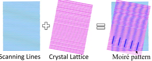
DOI: 10.4236/msce.2018.67002 9 Journal of Materials Science and Chemical Engineering technique is as follows: A moiré can be observed when the electron beam is fo-cused small enough, the scan periodicity of the STEM is close to the crystal plane spacing, and the scan direction is suitable for the crystal plane. It is called STEM moiré. The STEM moiré has the information of the crystal plane spacing. A schematic illustration of the STEM moiré is shown in Figure 1.
The research group of the University of Yamanashi also reported the experi-mental results about STEM moiré observation of Ge/Si (100) [13]. HREM Re-search Inc. and CEMES-CNRS developed an image analysis method to evaluate two dimensional lattice strains from the STEM moiré [14]. In this study, we produced a compositionally step-graded SiGe thin layers onto the Si (110) sub-strate, observed the STEM moiré, and calculated the slight change of the {111} plane spacing of the SiGe layers.
2. Experimental Procedure
A Si/SiGe/Si (110) hetero-structure was produced using the molecular beam ep-itaxy (MBE) method. We used an E-gun for Si and a K-cell for Ge. The substrate temperature was 600˚C. The deposition rate of Si was 0.5 Å/s. When the Si-Ge was deposited, the evaporation rate of Si was kept to 0.5 Å/s, and that of Ge was adjusted to produce a certain composition of Si-Ge solid solution. (Therefore, the total growth rate of the Si-Ge was slightly higher than 0.5 Å/s.) A composi-tionally uniform Si-Ge solid solution layer with the thickness of 440 nm was de-posited after forming the compositionally step-graded Si-Ge solid solution onto the Si (110) wafer. The compositionally graded region was added one-by-one in 9 steps and each step thickness was 40 nm. The designed Ge compositions of the Si-Ge layers were from 2 to 20 in atomic percent (Si0.98Ge0.02, Si0.96Ge0.04, ∙∙∙ Si0.8Ge0.2).
[image:2.595.243.507.601.707.2]The Ge-composition of the uniform SiGe layer was evaluated by X-ray reci-procal mapping (XRM). It was revealed that the Ge-composition was at about 22 at%. We intended to divide the Ge-composition from 2 to 20 at% by 2-at% steps as mentioned before. However, the Ge-composition of each layer might have slightly shifted to be Ge-rich. If we simply divide 22 at% into 10 layers, the Ge-composition becomes 22, 19.8, 17.6, 15.4, 13.2, 11, ∙∙∙, 4.4, 2.2. These are not reasonable expressions, because the significant figures of these values can be probably 2. Therefore, we expediently describe the compositional ratios as
Figure 1. A schematic illustration of the STEM moiré.
Moiré pattern
DOI: 10.4236/msce.2018.67002 10 Journal of Materials Science and Chemical Engineering Si0.78Ge0.22, Si0.80Ge0.20, Si0.82Ge0.18, Si0.85Ge0.15, ∙∙∙, Si0.96Ge0.04, Si0.98Ge0.20. The stacking of the Si and SiGe layers is shown in Figure 2.
After the MBE growth and the XRF measurements, we deposited protection layers onto the annealed specimen to avoid damage caused by the focused ion beam (FIB). First, we deposited an amorphous carbon onto the specimen by simple vacuum evaporation. Second, Pt-Pd alloy was deposited onto it by magnetron sputtering. Then the specimen was set into the FIB and W was depo-sited onto the Pt-Pd/C/Si/SiGe/Si (110) by ion-assisted chemical deposition. Af-ter preparing these protection layers, the specimen was thinned by the FIB (Hi-tachi FB-2100A) with an acceleration voltage of 40 kV for main fabrication and 10 kV for final cleaning. Then we observed the microstructure of the specimen using conventional TEM and STEM methods with an acceleration voltage of 200 kV. After that, we set up the STEM condition carefully and took STEM moiré. A field-emission type STEM (FEI Tecnai Osiris) without any Cs correctors was uti-lized. Then commercially available software sMoiré (HREM Research Inc.) was utilized in order to analyze the STEM moiré quantitatively [14].
3. Results and Discussion
Figure 3 is a STEM bright field high-resolution image taken from the SiGe area of the specimen. As we mentioned above, the incidental beam condition of the STEM must be very stable in order to record the STEM moiré. This high-resolution image is a proof of the perfect condition of the STEM. It is also clear in this figure that the scanning direction of the STEM, which is always ho-rizontal in the STEM images, is almost parallel to the {111} plane of the speci-men. Thus, it is clear that the STEM is well prepared to observe the STEM moiré.
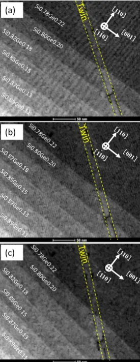
Figures 4(a)-(c) are three STEM bright field images taken at lower magnifi-cation than that in Figure 3. The STEM moiré patterns are clearly seen in these figures. The scan period of the incidental electron beam was 0.311 nm, which
Figure 2. A schematic illustration of the specimen.
Si0.89Ge0.11
Strained Si
Si (110)
Si0.78Ge0.22
Si0.80Ge0.20 Si0.82Ge0.18 Si0.85Ge0.15 Si0.87Ge0.13 Si0.91Ge0.09 Si0.93Ge0.07 Si0.96Ge0.04 Si0.98Ge0.02
20 nm
440 nm
DOI: 10.4236/msce.2018.67002 11 Journal of Materials Science and Chemical Engineering Figure 3. A STEM bright field high resolution image. It is mandatory to adjust the transmission electron microscope to the level that we can see STEM high resolution images, otherwise the STEM moiré cannot be observed.
Figure 4. A STEM bright field image. The STEM moiré between the scanning lines (scan period = 0.311 nm) and the {111} plane can be clearly seen. Scan rotation an-gle of (b) and (c) are −3 and −9 degrees in comparison with that of (a).
Si0.78Ge0.22
Si0.80Ge0.20
(a)
(b)
[image:4.595.305.443.321.678.2]DOI: 10.4236/msce.2018.67002 12 Journal of Materials Science and Chemical Engineering was close to the spacing of {111} planes of the Si and Ge. In general, moiré pat-terns drastically changes their appearances when their relative directions slightly changes. In the cases of Figure 4, we slightly changed the STEM rotation angle, which provides scan direction to the specimen. The STEM rotation angles of Figures 4(a)-(c) are 0, −3, −9 degrees, respectively. Because of these differences of STEM condition, the moiré patterns changed their directions and periodici-ties. This is a typical feature of the moiré.
Figure 5 is a FFT datum derived from the image shown in Figure 4(c) using the software sMoiré [14]. Reciprocals of scan spacing, lattice spacing, and moiré spacing are shown in this figure. In Figure 4(c), there is a twin and the moiré patterns across the twin show slightly different directions. According to this fact, the moiré spots in Figure 5 are split.
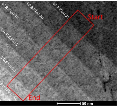
Figure 6 is the enlarged image of a part of Figure 4(c). The image analysis software “sMoiré” (HREM Research Inc.) was utilized to calculate the lattice spacing from this STEM moiré. This software was developed in order to evaluate the two dimensional lattice strains from the STEM moiré [14]. In this study, we used this software to calculate one dimensional changes of the {111} crystal plane spacing. Essentially, FFT was applied to the moiré and the spacing of the {111} planes from each layer were calculated from the FFT results.
[image:5.595.310.437.414.666.2]Figure 7 is the result of the image analysis for the moiré shown in Figure 6. The change of the {111} spacing with changing the positon in the specimen was plotted. We expected to detect how it is changing according to the Ge-concentration.
Figure 5. A FFT datum derived from the image shown in Figure 4(c) using the software sMoiré [14]. Three arrows can be interpreted as reciprocals of scan spacing, lattice spac-ing, and moiré spacing. The moiré spots are split because the moiré changes its direction across the twin in the area of Figure 4(c).
Scan
spacing
Lattice
spacing
DOI: 10.4236/msce.2018.67002 13 Journal of Materials Science and Chemical Engineering Figure 6. An enlarged image of Figure 4(c). The {111} space in the red rectangle area was calculated using the software sMoiré [14]. The result is shown in Figure 7.
Figure 7. The results of the image analysis. The horizontal axis is a distance on the spe-cimen. The direction is perpendicular to the interface of the each layer. The vertical axis is a change of the {111} spacing calculated from the moiré spacing using the software sMoiré [14].
the accurate value of the {111} spacing could not calculated yet for this specimen and there is an uncertainty of the calculated {111} spacing. However, the ten-dency of the changes of the {111} spacing, that is gradually decreases toward the low-Ge-concentration area, is qualitatively consistent with the expected inclina-tion. The reason of the uncertainty of the calculated {111} spacing in each layer might be the noise of the STEM images. We need further study to measure pre-cise value by using this technique.
4. Summary
We succeeded in observing the STEM moiré of the compositionally step-graded
Start
End
Distance from the starting point. (nm)
Re
la
tiv
e sp
ac
in
g
of
the
{111}
pl
ane
. (pm
[image:6.595.211.539.325.500.2]DOI: 10.4236/msce.2018.67002 14 Journal of Materials Science and Chemical Engineering SiGe/Si (110) without using a high-end model TEM. We also succeeded in cal-culating the slight change of the {111} spacing using the “sMoiré” (HREM Re-search Inc.) [14]. This technique, the combination of the STEM moiré observa-tion and the usage of the software sMoiré, has a potential to detect slight change of the lattice spacing from wider area, in comparison with other TEM-related techniques. However, we need further experimental efforts to take higher quality STEM moiré images which will realize better image analysis.
References
[1] Yamanaka, J., Sawano, K., Suzuki, K., Nakagawa, K., Ozawa, Y., Hattori, T. and Shiraki, Y. (2006) Dislocation Distribution in a Strain-Relaxed SiGe Thin Film Grown on an Ion-Implanted Si Substrate. Thin Solid Films, 508, 103-106.
https://doi.org/10.1016/j.tsf.2005.08.392
[2] Arimoto, K., Yamanaka, J., Nakagawa, K., Sawano, K., Shiraki, Y., Koh, S. and Usami, N. (2006) Determination of Lattice Parameters of SiGe/Si(110) Hetero-structures. Thin Solid Films, 508, 132-135. https://doi.org/10.1016/j.tsf.2005.08.412 [3] Arimoto, K., Watanabe, M., Yamanaka, J., Nakagawa, K., Sawano, K., Shiraki, Y., Usami, N. and Nakajima, K. (2009) Crystalline Morphologies of Step-Graded SiGe Layers Grown on Ex-Act and Vicinal (110) Si Substrates. J. Cryst. Growth, 311, 809-813. https://doi.org/10.1016/j.jcrysgro.2008.09.061
[4] Arimoto, K., Watanabe, M., Yamanaka, J., Nakagawa, K., Usami, N., Nakajima, K., Sawano, K. and Shiraki, Y. (2009) Strain Relaxation Mechanisms in Step-Graded SiGe/Si(110) Hetero-Structures Grown by Gas-Source MBE at High Temperatures. J. Cryst. Growth, 311, 819-824. https://doi.org/10.1016/j.jcrysgro.2008.09.064 [5] Yamanaka, J., Shirakura, M., Yamamoto, C., Utsuyama, N., Sato, K., Yamada, T.,
Hara, K.O., Arimoto, K. and Nakagawa, K. (2018) Surface Roughness of SiGe/Si (110) Formed by Stress-Induced Twins and the Solution to Produce Smooth Sur-face. Journal of Materials Science and Chemical Engineering, 6, 25-31.
https://doi.org/10.4236/msce.2018.61004
[6] Su, D. and Zhu, Y. (2010) Scanning Moiré Fringe Imaging by Scanning Transmis-sion Electron Microscopy. Ultramicroscopy, 110, 229-233.
https://doi.org/10.1016/j.ultramic.2009.11.015
[7] Kim, S., Lee, S., Oshima, Y., Kondo, Y., Okunishi, E., Endo, N., Jung, J., Byun, G., Lee, S. and Leeless, K. (2013) Scanning Moiré Fringe Imaging for Quantitative Strain Mapping in Semiconductor Devices. Appl. Phys. Lett., 102, 161604.
https://doi.org/10.1063/1.4803087
[8] Kim, S., Kondo, Y., Lee, K., Byun, G., Kim, J.J., Lee, S. and Lee, K. (2013) Quantita-tive Measurement of Strain Field in Strained-Channel-Transistor Arrays by Scan-ning Moiré Fringe Imaging. Applied Physics Letters, 103, 033523.
https://doi.org/10.1063/1.4816286
[9] Kim, S., Kim, J.J., Jung, Y., Lee, K., Byun, G., Hwang, K.H., Lee, S. and Lee, K. (2013) Reliable Strain Measurement in Transistor Arrays by Robust Scanning Transmission Electron Microscopy. AIP ADVANCES, 3, 092110.
https://doi.org/10.1063/1.4821278
[10] Kondo, Y. and Endo, N. (2014) Strain Analysis Using STEM Moiré Method. Ken-bikyo, 49, 226. (In Japanese)
DOI: 10.4236/msce.2018.67002 15 Journal of Materials Science and Chemical Engineering [12] Kim, S., Lee, S., Kondo, Y., Lee, K., Byun, G., Lee, S. and Lee, K. (2014) Strained
Hetero Interfaces in Si/SiGe/SiGe/SiGe Multi-Layers Studied by Scanning Moiré Fringe Imaging. Journal of Applied Physics, 114, 053518.
https://doi.org/10.1063/1.4817729
[13] Yamanaka, J., Yamamoto, C., Nakaie, H., Arai, T., Arimoto, K., Hara, K.O. and Nakagawa, K. (2017) STEM Moiré Observation of Lattice-Relaxed Germanium Grown on Silicon. Journal of Materials Science and Chemical Engineering, 5, 102-108. https://doi.org.10.4236/msce.2017.51014
![Figure 5. A FFT datum derived from the image shown in Figure 4(c) using the software sMoiré [14]](https://thumb-us.123doks.com/thumbv2/123dok_us/9282501.421894/5.595.310.437.414.666/figure-datum-derived-image-shown-figure-software-smoire.webp)
![2,4 Bis(4 butoxyphenyl) 3 azabicyclo[3 3 1]nonan 9 one](data:image/gif;base64,R0lGODlhAQABAIAAAP///wAAACH5BAEAAAAALAAAAAABAAEAAAICRAEAOw==)