TO EMPLOY SOA-BASED OPTICAL SSB
MODULATION TECHNIQUE IN FULL-DUPLEX ROF TRANSPORT SYSTEMS
C.-L. Ying
Department of Electronic Engineering Jinwen University of Science and Technology Taipei 231, Taiwan, Republic of China
H.-H. Lu
Institute of Electro-Optical Engineering National Taipei University of Technology Taipei 106, Taiwan, Republic of China
W.-S. Tsai
Department of Electrical Engineering Mingchi University of Technology Taipei 243, Taiwan, Republic of China
H.-C. Peng and C.-H. Lee
Institute of Electro-Optical Engineering National Taipei University of Technology Taipei 106, Taiwan, Republic of China
Abstract—A full-duplex radio-over-fiber (ROF) transport system employing semiconductor optical amplifier (SOA)-based optical single sideband (SSB) modulation technique is proposed and demonstrated. For our proposed approach, it is relatively simple to implement as it requires only one SOA to generate optical SSB signal. Over an-80 km single-mode fiber (SMF) transmission, low bit error rate (BER), clear eye diagram, and low third-order intermodulation distortion to carrier ratio (IMD3/C) were achieved. Our proposed full-duplex ROF transport systems are suitable for the long-haul microwave optical links.
1. INTRODUCTION
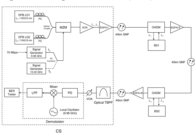
40km SMF Signal Generator 9.98 GHz Signal Generator 10.02 GHz f1 f2 RF Combiner CS DFB LD1
11533.6 nm
DFB LD2
2 1542.8 nm Optical Coupler
40km SMF 1
OADM 1 BS1 EDFA-III 40km SMF 70 Mbps 2 OADM 2 BS2 EDFA-II PC PC 1 2 Optical TBPF PD VOA BER Tester Mixer Local Oscillator (9.98 GHz) LPF Demodulator
MZM SOA EDFA-I
λ= = λ λ λ, λ λ λ λ
Figure 1. The experimental configuration of our proposed full-duplex ROF transport systems.
2. EXPERIMENTAL SETUP
Figure 1 shows the experimental configuration of our proposed full-duplex ROF transport systems employing SOA-based optical SSB modulation technique. For down-link transmission, the central station (CS) is composed of two distributed feedback laser diodes (DFB LDs), one MZM, one SOA, one erbium-doped fiber amplifier (EDFA), and two microwave signal generators. Between the two DFB LDs and the 2×1 optical coupler are the polarization controllers (PCs). The PCs are for polarization-dependent characteristic of MZM. The central wavelengths of these two DFB LDs are 1533.6 nm (λ1) and 1542.8 nm (λ2), respectively. Two DFB LDs provided two optical carriers to the MZM, and a low bias voltage was applied to the MZM. The optical signals of the MZM were coupled into the SOA to generate optical SSB signals.
links. At the CS, the optical signals are generated and then distributed through standard SMF to the remote base stations (BSs) (BS1 and BS2) by using cascaded EDFAs and optical add-drop multiplexers (OADMs). The optical signals are transmitted through three SMF spans (40 km × 3) with the help of three EDFAs. Each BS is connected to the fiber backbone through an OADM which deals with an individual wavelength. The appropriate wavelengths are dropped by the OADM in BSs. The OADM, with >40 dB add/drop channel isolation, consists of one fiber Bragg grating (FBG) located between two optical circulators (OCs). The functions of OADM are to drop the down-link wavelength to the BS from the fiber backbone, and to add the up-link wavelength to the fiber backbone from the BS. The optical signal is modulated by 70 Mbps/9.98 GHz data signal through a MZM, and passed through an SOA to generate the optical SSB-modulated signal. The down-link data signal is adjusted by a variable optical attenuator (VOA), and detected by a broadband photodiode (PD) to convert optical signal into RF one. The 70 Mbps/9.98 GHz data signal is fed into a BER tester for BER analysis after demodulation. For up-link transmission, the 70 Mbps/9.98 GHz data signal is transmitted through SMF to the CS, passed through an optical tunable band-pass filter (TBPF) to select the desired wavelength, attenuated by a VOA, detected by a PD to convert optical signal into RF one, and provided to a demodulator. For demodulation part, RF and local oscillator (9.98 GHz) signals are applied to a mixer, the output of the mixer is put through a low-pass filter (LPF) to obtain the data stream (70 Mbps). Finally, 70-Mbps data stream is fed into a BER tester for BER analysis. As to the IMD3/C value measurement, an additional microwave carrier (f2 = 10.02 GHz) is added in CS to provide two-tone signal measurement. The IMD3/C value is measured by using a spectrum analyzer.
3. EXPERIMENTAL RESULTS AND DISCUSSION
(XPM) interaction [11]. XPM interaction between optical channels will induce intolerable amounts of distortions in WDM-ROF systems, in which deteriorating the performances of systems. Thereby, for better performances, our proposed systems can exploit the available bandwidth of 1530–1550 nm to address maximum multiple BSs with 4 nm channel spacing.
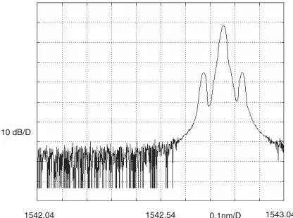
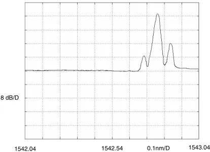
Figure 2a shows the optical DSB-modulated signal (1533.6 nm,
λ1) in an optical spectrum analyzer (OSA) at the SOA input, both sidebands are 9.98 GHz (∼0.08 nm) away from the optical carrier. Figures 2b and 2c show the optical SSB-modulated signals in an OSA at the SOA output. And further, Figure 2d shows the optical
10 dB/D
1532.84 1533.34 0.1nm/D 1533.84
Figure 2a. The optical DSB-modulated signal (1533.6 nm,λ1) at the SOA input.
8 dB/D
1532.84 1533.34 0.1nm/D 1533.84
8 dB/D
1532.84 1533.34 0.1nm/D 1533.84
Figure 2c. The optical SSB-modulated signal in an OSA at the SOA output (SOA input optical power is−15 dBm per wavelength).
10 dB/D
1542.04 1542.54 0.1nm/D 1543.04
Figure 2d. The optical DSB-modulated signal (1542.8 nm,λ2) at the SOA input.
8 dB/D
1542.04 1542.54 0.1nm/D 1543.04
Figure 2e. The optical SSB-modulated signal in an OSA at the SOA output (SOA input optical power is−10 dBm per wavelength).
8 dB/D
1542.04 1542.54 0.1nm/D 1543.04
Figure 2f. The optical SSB-modulated signal in an OSA at the SOA output (SOA input optical power is−15 dBm per wavelength).
at each BS. When the optical DSB signal was coupled into the SOA at the input power of −10∼ −15 dBm per wavelength, there was a large change in the optical signal at the SOA output. The amplitude of the optical sideband at the right-hand side of the optical carrier was not changed, but the amplitude of the optical sideband at the left-hand side of the optical carrier was suppressed, i.e., the optical SSB signal was created. In this proposed systems, optical SSB signal was created and transmitted as the SOA input optical power was −10 dBm per wavelength (λ1 and λ2).
(a)
-23 -18 -13 -8 -3 2
Received Optical Power (dBm)
Down-Link BER
back-to-back (for DSB modulation) optical SSB system
optical DSB system
(b)
-23 -18 -13 -8 -3 2
Received Optical Power (dBm)
Up-Link BER
optical SSB system
optical DSB system
10-6
10-7
10-8
10-9
10-10
10-11
10-12
10-5 10-6
10-7
10-8
10-9
10-10
10-11
10-12 10-5
Figure 3. (a) The measured down-link BER curves of 70 Mbps/9.98 GHz data channel (CS→BS2), (b) The measured up-link BER curves of 70 Mbps/9.98 GHz data channel (BS1→CS).
in the SOA, the electrical field of the output signal in an SOA can be expressed as [10]:
E(t) =E0
1 +m
2 sin(ωmt)
·exp
iω0t+ (1 +iα)m
2ηPeff sin(ωmt+β)
Table 1. The power level differences between the carrier and the upper sideband forλ1 at the SOA output at different input optical power per wavelength. Input Optical Power (dBm) Power Level Difference (dB) -8 -9 -10 -11 -12 -13 -14 -15 -16 -17 -18 25.3 26.2 27 26.5 25.8 25.2 24.5 24 22.7 21.4 20
effective input optical power, and β is the phase difference between the change of carrier density and the change of input optical power. Expanding Equation (1) in Bessel series and neglecting high-order terms, the complex envelopes for the frequencies ω0 +ωm (upper sideband) andω0−ωm (lower sideband) can be estimated as:
Eω0±ωm ≈ ∓im
4 E0J0(χ)· {1 +ρexp[j(θ±β)]} (2)
where θ = tan−1α, ρ =ηPeff(1 +α2)1/2, and χ = −imρ2exp(iθ). Then sideband suppression ratio (SSR) can be derived:
SSR =E
ω0−ωm Eω0+ωm
2 ≈ 1 +ρexp[j(θ−β)]
1−ρexp[j(θ+β−π)
2 (3)
ρ is adjustable as a function of input optical power. Thereby, as
ρcos(θ+β−π) = 1, i.e., when
Peff = (1 +α2)−1/2ηcos[tan−1α−tan−1(ωmτeff)]−1 (4)
can be seen that the power level differences of 20∼27 dB are achieved. As optimal optical powers are launched (−10 dBm per wavelength), the maximum power level difference of 27 dB is obtained. Under this condition, it corresponds with Equation (3) as denominator is approached to zero.
(a)
(b)
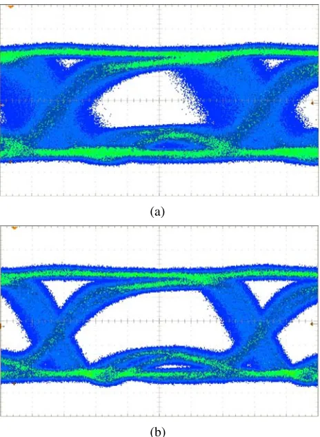
Figure 4. (a) The eye diagram of 70 Mbps/9.98 GHz data stream for optical DSB system, (b) The eye diagram of 70 Mbps/9.98 GHz data stream for optical SSB system.
The measured down-link BER curves of 70 Mbps/9.98 GHz data channel (CS→BS2) are presented in Figure 3(a). At a BER of 10−9; for optical DSB system, the received optical power level is
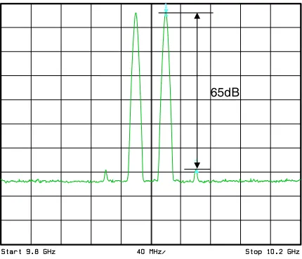
65dB
Figure 5. Electrical spectrum of the received signal with SOA-based optical SSB system.
the measured up-link BER curves of 70 Mbps/9.98 GHz data channel (BS1→CS) are presented in Figure 3(b). At a BER of 10−9; for optical DSB system, the received optical power level is −2.8 dBm; for SOA-based optical SSB system, the received optical power level is −18.8 dBm. Receiver sensitivity improvement of 16 dB is obtained as SSB modulation technique is employed. From Figure 3(a) we also can see that, at a BER of 10−9, there exists a large power penalty of 17.1 dB between the back-to-back case (for DSB modulation) and the optical DSB system. But, at a BER of 10−9, SOA-based optical SSB system exhibits a power penalty of only 0.8 dB. The BER is given by
BER= 1
2erfc
SNR
2 (5)
where SNR is systems’ signal-to-noise ratio. Carrier power reduction will be reduced greatly as SOA-based optical SSB modulation technique is employed. The higher carrier power level we get, the higher SNR value we achieve. SOA-based optical SSB system increases the SNR value of system significantly, in which causing system with better BER performance, and leading to a large improvement of receiver sensitivity.
in optical DSB system (Figure 4(a)). DSB signal suffers fading prob-lem due to fiber dispersion, in which resulting in the amplitude and jitter of eye diagram increase greatly. However, in SOA-based optical SSB system, clear eye diagram is obtained (Figure 4(b)). Electrical spectrum of the received signal with SOA-based optical SSB system is shown in Figure 5. It is obvious that the residue IMD3/C level of
−65 dBc or more is obtained. Carrier power degradation will be re-duced as optical SSB modulation technique is employed, leading to an improvement of IMD3/C value.
4. CONCLUSION
Full-duplex ROF transport systems employing SOA-based optical SSB modulation technique is proposed and demonstrated. Our proposed approach is relatively easy to implement, as it requires only one SOA to generate optical SSB signal. Over an-80 km SMF transmission, low BER, clear eye diagram, and low IMD3/C were obtained. Our proposed full-duplex ROF transport systems are suitable for the long-haul microwave optical links.
REFERENCES
1. Serdyuk, V. M., “Dielectric study of bound water in grain at radio and microwave frequencies,” Progress In Electromagnetics
Research, PIER 84, 379–406, 2008.
2. Lin, C. T., J. Chen, P. C. Peng, C. F. Peng, W. R. Peng, B. S. Chiou, and S. Chi, “Hybrid optical access network integrating fiber-to-the-home and radio-over-fiber systems,”IEEE
Photon. Technol. Lett., Vol. 19, 610–612, 2007.
3. Oraizi, H. and S. Hosseinzadeh, “A novel marching algorithm for radio wave propagation modeling over rough surfaces,” Progress
In Electromagnetics Research, PIER 57, 85–100, 2006.
4. Prat, J., M. C. Santos, and M. Omella, “Square root module to combat dispersion-induced nonlinear distortion in radio-over-fiber systems,”IEEE Photon. Technol. Lett., Vol. 18, 1928–1930, 2006. 5. Blais, S. R. and J. Yao, “Optical single sideband modulation using an ultranarrow dual-transmission-band fiber bragg grating,”IEEE
Photon. Technol. Lett., Vol. 18, 2230–2232, 2006.
7. Sung, H. K., E. K. Lau, and M. C. Wu, “Optical single sideband modulation using strong optical injection-locked semiconductor lasers,”IEEE Photon. Technol. Lett., Vol. 19, 1005–1007, 2007. 8. Smith, G. H., D. Novak, and Z. Ahmed, “Overcoming
chromatic-dispersion effects in fiber-wireless systems incorporating external modulator,”IEEE Trans. Microwave Theory Tech., Vol. 45, 1410– 1415, 1997.
9. Davies, B. and J. Conrad, “Hybrid modulator structure for subcarrier and harmonic subcarrier optical single sideband,”IEEE
Photon. Technol. Lett., Vol. 10, 600–602, 1998.
10. Lee, U. S., H. D. Jung, and S. K. Han, “Optical single sideband signal generation using phase modulation of semiconductor optical amplifier,”IEEE Photon. Technol. Lett., Vol. 16, 1373–1375, 2004. 11. Lu, H. H., W. J. Wang, and W. S. Tsai, “CSO/CTB performances improvement in a bi-directional DWDM CATV system,” IEEE