ISSN 2348 – 7968
610
Calculations of DOS and electronic structure in Bi₂S₃ and Bi₂Se₃
by using FP-LAPW method
Dandeswar Deka
1, A. Rahman
1and R. K. Thapa
Department of Physics, Condensed Matter Theory Research Group, Mizoram University, Aizawl 796 004, Mizoram
1
Department of Physics, Gauhati University, Guwahati 781014
Email: [email protected]
Abstract
The electronic structures for Bi₂S₃ and Bi₂Se₃ have been investigated by first principles full potential- linearized augmented plane wave (FP-LAPW) method with Generalized Gradient Approximation (GGA). The calculated density of states (DOS) and band structures show semiconducting behavior of Bi₂S₃ and Bi₂Se₃ with a narrow indirect energy band gap of 1.4 eV in Bi₂S₃ and 0.8 eV in Bi₂Se₃ .
Keywords
: DFT, FP-LAPW, DOS, energy band structure, energy band gap.PACS:
71.15.-m, 71.15.Dx, 71.15.Mb, 71.20.-b, 75.10.-b1. INTRODUCTION
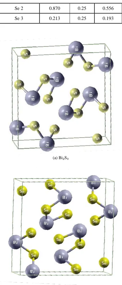
Today semiconductors can be grown with various compositions from monoatomic layer to nano-scale islands, rows, arrays, in the art of quantum technologies and the numbers of conceivable new electronic devices are manufactured [1]. Narrow gap semiconductors Bi₂S₃ and Bi₂Se₃ are classic room temperature thermoelectric materials[2]. These are the chalcogenides of poor metal having important technological applications in optoelectronic nano devices [3], field-emission electronic devices [4], photo-detectors and photo-electronic devices [5] and photovoltaic convertors, thermoelectric cooling technologies based on the Peltier effect [6,7]. They have orthorhombic crystal structures at room temperature with x, y and z- positions of atoms [8] as given in Table:1 and space group Pnma (number 62) . The crystal structures of Bi₂S₃ and Bi₂Se₃ are illustrated in Fig.1(a-b). In this report, we would like to present a systematic study of DOS and energy band structures of Bi₂S₃ and Bi₂Se₃ using FP-LAPW method.
Table 1: x, y and z-positions of atoms of Bi₂S₃ and Bi₂Se₃
Atom (Bi₂S₃) X Y Z
Bi 1 0.0164 0.25 0.6745
Bi 2 0.3406 0.25 0.4661
S 1 0.0494 0.25 0.1311
S 2 0.3773 0.25 0.0604
S 3 0.2165 0.25 0.8069
Atom (Bi₂Se₃) X Y Z
Bi 1 0.012 0.25 0.328
Bi 2 0.343 0.25 0.534
Se 1 0.067 0.25 0.876
Se 2 0.870 0.25 0.556
Se 3 0.213 0.25 0.193
(a) Bi₂S₃
2. T
First theor struc Burk corre as a theor calcu Murn calcu of sta wher modu of th volum show optim Å an c=11 using funct harm and consi the a funct with value Se: 4 state were radii Rmt = k-poi lattic b= 3 3.964 Fig.2 TableTh b Expa po T
Fig.1 : U
HEORY AND
principles FP-L ry ( DFT) ) is cture of Bi₂S₃. T ke and Ernzerh elation potentials function of the retical lattice c ulated by fitti naghan’s equati ulations as a fun ates according to
re is the m ulus at the equil he bulk modulus me is given by wn in Fig.2(a-b) mized using the e nd c= 11.129 Å 1.62 Å for Bi₂Se
g the WIEN2K c tions, charge de monics within no
in the remainin idered. The max atomic spheres tions in the inte
a cut-off of to K
e of the wave v 4s, 4p states wer s were treated a e expanded upto are set to Rmt = = 2.3 a.u. for Bi
ints was used ce constants foun
.567 Å and c= 47 Å and c= 1 2(a-b).
e 2: The parameter
PARAME
he plane-wave cu basis functions ,
ansion of wave f otentials inside t
The potential, ch
(b) Bi₂Se Unit cell structures
D COMPUTA
LAPW [9] metho s used for calc The version of G hof [10] was u
s. The calculated volume (V) we constants. Equil
ing the calcul ion of state [11 nction of volume o Murnaghan.
′
′ 1
minimum energy librium volume s at the equilibri the correspondi ) [12]. The equ experimental va for Bi₂S₃, and e₃ [8]. The calc code [13]. In the nsity and potent on overlapping ng space of th ximum multi-po
was confined rstitial region w
Kmax=2.5 a.u.-1 vector K=k+G).
re treated as val as core state. The o a cut-off Gmax 2.4 a.u. for Bi a and 2.2 a.u. for after doing k-nd by volume op
11.0868 Å for 1.2716 Å for
rs chosen for the c
ETERS
ut-off for the RMT x Kmax
functions,density the RMT , lmax
harge density
e₃
of Bi₂S₃ and bi₂S
ATIONAL ME
od based on dens culations of DO GGA as prescribe
used for the e d total energy (E ere used for det librium lattice lated total en 1]. A series of e can be fitted t
′ 1 1
y at T = 0K, and ′ is press ium volume. Th ing total energy uilibrium lattice
lues of a=11.269 d a= 11.83 Å, b culation was acc e FP-LAPW pro
tial are expande atomic spheres e unit cell plan olarity l for the within lmax= 1 were expanded in
(where Kmax is For Bi: 6s, 6p, ance state and a e potential and c
x = 12 a.u.-1. Th and 2.2 a.u. for S Se in Bi₂Se₃. A optimization. T ptimization are a Bi₂S₃, and a=1 Bi₂Se₃ which
computation of Bi₂
VALUE y, 12 e₃
ETHODS
sity functional OS and band ed by Perdew, exchange and E) within GGAtermination of constants are nergy to the
total energy to an equation
1
is the bulk sure derivative he equilibrium y minimum as constant was 9 Å, b=3.9717 b=4.09 Å and complished by ocedure , wave ed in spherical of radius Rmt ne waves are
waves inside 0. The wave n plane waves
the maximum S: 3s, 3p and all other lower charge density he muffin- tin S in Bi₂S₃ and mesh of 1500 The calculated
a= 11.2263 Å, 11.4753 Å, b= are shown in
₂S₃ and Bi₂S₃
ES USED
7
10
a.u.-1.
exp Numb Fig. 2
3. RES
In Fig.2 cell vol plots of Fig.3, w 6p and electron formed around at arou conduct contribupanded upto cut
ber of plane wav
Wave vector
RMT used
2: Energy versus V met
SULTS AND D
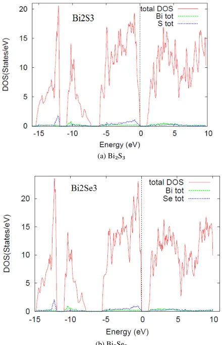
2(a-b), we show lume for Bi₂S₃ f Bi₂S₃ and Bi we found that the S-3p electron s n states in Bi₂Se₃
by 6s and 6p e -10.5 eV is obs und -10.2 eV tion region, wh uted by Bi-6p, 6
t-off ,Gmax
ves generated
r, k
d
(a) Bi₂S₃
(b) Bi₂Se₃ Volume curve usin thod for Bi₂S₃and
DISCUSSION
the total energy and Bi₂Se₃. T i₂Se₃ are shown e contributions t states in Bi₂S₃ a
₃. The core regio electron states o served in Bi₂S₃[ V is observed hich is above th 6px, 6py state el
ISSN
729
1500
Bi = 2.4 a.u., S ( for Bi Bi = 2.3 a.u.,S ( for Bi₂
₃
ng the volume opti Bi₂Se₃
NS
curve as a funct The total and pa n in Figs.3,4,5 & to total DOS wer and from Bi-6p on which is belo of Bi and a shar
[Fig.4(a)] and a in Bi₂Se₃[Fig.4 he Fermi level, lectrons in Bi₂S
2348 – 7968
611
9
0
S = 2.2 a.u.
₂S₃) Se= 2.2 a.u.
₂Se₃)
imization
tion of unit artial DOS & 6. From re from
Bi-and Se-4p w -6eV is rp peak at
ISSN 2348 – 7968
612
and by Bi-6p, 6px state electrons in Bi₂Se₃[Fig.5(b)]. In the valence region (below Fermi level), we have observed, S–3p electronstate is mainly contributing to total DOS giving a sharp peak at around -0.8eV in Bi₂S₃ [Fig.6(a)] and Se–4p electronstate is mainly contributing to total DOS giving sharp peaks at around -0.5eV and -1.2eV in Bi₂Se₃ [Fig.6(b)].
(a) Bi₂S₃
(b) Bi₂Se₃
Fig. 3: Bi₂S₃-total, Bi-total and S-total and Bi₂Se₃-total, Bi-total and Se-total (Energy= 0 eV, corresponds to Fermi level)
(a) Bi₂S₃
(b) Bi₂Se₃
Fig. 4 : Total DOS, Bi-total & S-total statesofBi₂S₃ and Total DOS, Bi-total & Se-Bi-total states ofBi₂Se₃
(a) Bi₂S₃
(b) Bi₂Se₃
Fig.5: Bi-total, Bi-p, px & py states of Bi₂S₃ and Bi-total, Bi-s, p & px
Fig.6
From of th of th plots wher comp and f
6: S-total, S-s & S
m the band struc he order of 1.4 e he order of 0.8 s were also foun re peaks of the pared band struc found that highe
(a) Bi₂S
(b) Bi₂Se S-p States of Bi₂S₃ States of Bi
cture plots, we o V in Bi₂S₃[Fig. eV in Bi₂Se₃[F d with higher nu DOS were obse ctures with DO
r DOS regions c
(a) Bi₂S
₃
e₃
and Se-total, Se-s
₂Se₃
observed an indi 7(a)]and an indi Fig.7(b)]. The b umber of bands erved. In Fig.8 S plots of Bi₂S correspond to mo
S₃
s, Se-p & Se-px
irect band gap irect band gap band structure at the regions & 9 we have
₃ and Bi₂Se₃, ore bands.
Fig.8:
Fig.9: B
4. CON
In conc theoreti
Fig.7: The plots o
Band structure of corre
Band structure of B corre
NCLUSIONS
lusion, we have cal and experim
(b) Bi₂Se₃ of band structures
Bi₂S₃ combined w sponds to Fermi L
Bi₂Se₃ combined w sponds to Fermi L
observed a qua mental lattice c
ISSN
of Bi₂S₃ and Bi₂
with DOS plot (En Level, E)
with DOS plot (En Level, E)
litative agreeme constants. Calcu
2348 – 7968
613
Se₃
nergy=0eV
nergy=0eV
ISSN 2348 – 7968
614
gap is very close to experimental value. Band gaps of the order of 1.4 eV and 0.8eV suggest that Bi₂S₃ and Bi₂Se₃ are semiconductors with low energy gap. Since Fermi level is very close to valance band, it indicates that the semiconductors are p-type. The calculated band gaps also suggest that the compounds may be used as suitable candidate for thermoelectric applications. The semiconductor Bi₂S₃ with band gap 1.4eV belongs to a family of solid state materials with applications in thermoelectric cooling technologies based on the Peltier effect [14,15]. The semiconductor Bi₂Se₃ with band gap 0.8eV has useful applications in the field of thermoelectric devices as solid state coolers or generators [16,17]. However, the band gaps when checked with experimental values (1.3eV in Bi₂S₃ and 0.8eV in Bi₂Se₃) [14] seem to have differences. We propose to check these discrepancies with mBJ potential inclusion.
ACKNOWLEDGEMENTS
DD is grateful to Department of Physics, Gauhati University and Department of Physics, Mizoram University for extending all the necessary facilities for doing this work. RKT acknowledges a research grant from UGC.
REFERENCES
[1] E. Erbarut, Solid State Communications, 127, 515-519 (2003).
[2] M.G. Kanatzidis, Semiconductors and Semimetals, 69, 51 (2001).
[3] H. Bao, X. Cui, C. Li, Y. Gan, J. Zhang and J. Guo Photoswitchable Semiconductor Bismuth Sulfide (Bi2 S3) Nanowires and Their Self-Supported Nanowire Arrays , J. Phys. Chem. C, 111(33), 12279-12283 (2007).
[4] Y. Yu, C. H. Jin, R. H. Wang, Q. Chen and L. M. Peng, High Quality Ultralong Bi2 S3 Nanowires : Structure, Growth and Properties , J. Phys. Chem. B, 109(40), 18772-18776 (2005). [5] L. Li, R. Cao, Z. Wang, J. Li and L. Qi, Template Synthesis
of Hierarchical Bi2 E3 (E= S, Se, Te) Core-Shell microspheres and Their Electrochemical and Photoresponsive Properties, J. Phys. Chem. C, 113(42), 18075-18081 (2009).
[6] B. Miller, A. Heller, Semiconductor liquid junction solar cells based on anodic sulphide films, Nature262, 680-681 (1976).
[7] O. Rabin, J.M. Perez, J. Grimm, G. Wojtkiewicz, R. Weissleder, An X-ray computed tomography imaging agent based on long- circulating bismuth sulphide nanoparticles,
Nat. Mater. 5, 118 (2006).
[8] L. F. Lundegaard, E. Makovicky, T. Boffa Ballaran and T. Balic-Zunic, Crystal structure and cation lone electron pair activity of Bi2 S3 between 0 and 10 GPa Physics and
Chemistry of Minerals32, 578-584 (2005).
[9] R. K.Thapa, Sandeep, M. P. Ghimire and Lalmuanpuia, Study of DOS and energy band structures in beryllium chalcogenides, Indian J. Phys.85, 727-736 (2011).
[10] J. P. Perdew, K. Burke and M. Ernzerhof, Generalized Gradient Approximation Made Simple, Phys. Rev. Lett., 77, 3865 (1996).
[11] F. D. Murnaghan, The compressibility of media under extreme pressures, Proc. Natl. Acad. Sci. USA 30, 244-247 (1944).
[12] P. Schwartz and P. Blaha, Fifth World Congress on Computational Mechanics, Vienna, Austria (1903).
[13] P. Blaha, K. Schwarz, G. Madsen, D. Kvasnicka and J. Luitz, An Augmented Plane Wave Plus Local Orbitals Program for calculating Crystal Properties (Tech. University, Vienna-Austria) (2001).
[14] J. Black, E. M. Conwell, L. Seigle and C. W. Spencer,Electrical and optical properties of some M2V-BN3VI-B semiconductors, J. Physics and Chemistry of Solids 2(3), 240-251, (1957).
[15] X. S. Peng, G. W. Meng, J. Zhang , L. X. Zhao, X. F. Wang, Y. W. Wang, L. P. Zhang, Electrochemical fabrication of ordered Bi2 S3 nanowire arrays, J. Phy. D: Appl. Phys. 34, 3224(2001).
[16] D. M. Rowe, CRC Hand book of Thermoelectrics, CRC press, Boca Ratou, FL, 90 (1995).
[17] H. J. Goldsmith, Thermoelectric Refrigeration, Pion Ltd., London (1986).