10.15662/ijareeie.2014.0308025
Copyright to IJAREEIE www.ijareeie.com 11155
Analysis, Simulation of 3-Stage
Cockcroft-Walton Voltage Multiplier for High Step-Up
Dc-Dc Converter
M.N.Karthikeyan
1, R.P.Pandu
2,M.Gopisivaprasad
3, G.Seshadri
4PG Student [PE], Dept. of EEE, Siddharth institute of Engineering & technology, Puttur, Andhrapradesh, India1
PG Student [PE], Dept. of EEE, Siddharth institute of Engineering & technology, Puttur, Andhrapradesh, India2
Associate professor, Dept. of EEE, Siddharth institute of Engineering & technology, Puttur, Andhrapradesh, India3
Associate professor, Dept. of EEE, Siddharth institute of Engineering & technology, Puttur, Andhrapradesh, India4
ABSTRACT: This paper presents a high step-up dc-dc converter based on the Cockcroft-Walton (CW) voltage multiplier without using step-up transformer. The proposed converter is quite suitable for applying low-input dc voltage, to high output dc voltage dc generation systems. It provides continuous input current to load with low ripple voltage and current. Voltage stress on the all switching device, diodes, and capacitors are lower than the other type. Moreover, based on the 3-stage Cockcroft-Walton (CW) voltage multiplier, the proposed converter can provide a suitable dc source is solar cells, fuel cell and other type source for a 3-stage multilevel inverter. In this paper, the control strategy employs two independent frequencies, one operates at high frequency to minimize the size of the inductor and other one operates at relatively low frequency to the desired output voltage ripple. The simulation is carried over by the MATLAB-SIMULINK.
KEYWORDS: Cockcroft-Walton (CW) voltage multiplier.
I.INTRODUCTION
In generally to get high dc output voltage we are using voltage multipliers, DC-AC-DC inverters With step-up transformer due to using of transformers the size, cost and high ripples are present in output voltage and current. The Cockcroft–Walton (CW) generator, or multiplier, which is an electronic circuit it generates a high DC voltage from a low level input voltage AC or pulsing DC. Today Cockcroft-Walton (CW) circuits are still used in particle accelerators, and also in many electronic devices where high voltages require. The Applications are x-ray machines, television, and photocopiers. It is made up of ladder network of capacitors and diodes to generate high DC voltages. Here we are using only capacitors and diodes, these voltage multipliers can step up relatively low voltages to extremely high voltage, while at the same time lighter and cheaper than using step-up transformers. The biggest advantage of such circuits is that the voltage across each stage of the cascade is equal to only twice the peak input voltage in a half wave rectifier. It has the advantage of requiring relatively low cost components and easy to insulate. Possibility of taking output from any stage, like a multi tapped transformer.
LITERATURE SURVEY: Review of nonisolated high-step-up dc/dc converters in photovoltaic grid-connected applications,” by W. Li and X. He, IEEE Trans. Ind. Electron., vol. 58, no. 4, pp. 1239–1250, Apr. 2011.
How to achieve high-step-up, low-cost, and high-efficiency dc/dc conversion is the major consideration due to the low PV output voltage with the parallel-connected structure. Providing continuous input current with low ripple, high voltage ratio and low voltage stress on the switches, diodes and capacitors.
10.15662/ijareeie.2014.0308025
Copyright to IJAREEIE www.ijareeie.com 11156
Presents New residential scale photovoltaic (PV) arrays are commonly connected to the grid by a single DC-AC inverter connected to a series string of PV modules, or many small DC-AC inverters which connect one or two modules directly to the AC grid.
II.PROPOSED CIRCUIT
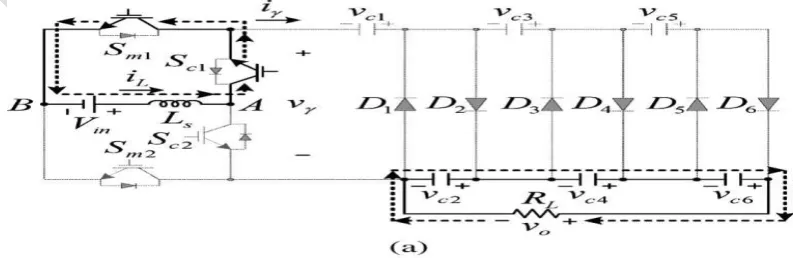
In this paper, proposed converter supplied by a low-level dc source, such as battery, PV module, or fuel cells. The proposed converter (Cockcroft–Walton (CW) generator, or multiplier) consists of one inductor Ls(boost inductor), four switches (Sm1, Sm2, Sc1, and Sc2) the rating of all switches are same as well as voltage stress across each switches are same, and one n-stage CW voltage multiplier The four switches are divided into two groups Sm1 (Sc1) and Sm2(Sc2) which operate in complementary mode, and they are operating under two different frequencies of Sm1 and Sc1 are defined as fsm and fsc, respectively. For convenience, fsm is denoted as modulation frequency, and fsc is denoted as alternating frequency. The both fsm and fsc frequencies should be as high as possible so that we can use smaller inductor and capacitors in this circuit. In this paper, fsm (=60 kHz) is set much higher than fsc (=1 kHz), and the output voltage is regulated by controlling by the duty cycle of Sm1 and Sm2, while the output voltage ripple can be adjusted by fsc. As shown in Fig.1, the well-known CW voltage multiplier is constructed by a cascade of stages with each stage containing six capacitors (C1, C2, C3, C4, C5, C6,) and six diodes (D1, D2, D3, D4, D5, D6,). In an n-stage CW voltage multiplier, there are N (= 2n) capacitors and N diodes n=3 (3-stage).
Fig. 1 3-Stage Cockcroft-Walton voltage multiplier.
III.OPERATTION
The operation of 3-stage Cockcroft-Walton (CW) Voltage Multiplier is divided to four mode operation is explained by the given below circuit diagrams from Fig. a to Fig. h
10.15662/ijareeie.2014.0308025
10.15662/ijareeie.2014.0308025
Copyright to IJAREEIE www.ijareeie.com 11158 Mode 3:Sm2 and Sc2 Switches are turned on, and Sm1, Sc1, and all CW diodes are turned off, as shown in Fig (e). The boost inductor Ls is get charged by the Vin dc source, the even group capacitors C6, C4, and C2 supply the load current, and the odd-group capacitors C5, C3, and C1 are not in conduction.
Mode 4: Sm1 and Sc2 Switches are turned on, Sm2 and Sc1 Switches are turned off, and the current iγ is negative. The boost inductor Ls and input Vin dc source are in series the boosted voltage is “-Vγ” transfer energy to the CW voltage multiplier through odd diodes, mode 4-A, show in fig (f) diode D5 is conducting. Thus, the even-group capacitors, except C6 which supplies load current, are discharged, and the odd-group capacitors C5, C3, and C1 are charged by iγ. mode- 4-B, D3 is conducting. Thus, C2 is discharged, C3 and C1 are charged by iγ, C6 and C4 supply load current, and C5 is not in conduction. Is shown In Fig (g), mode-4-C, D1 is conducting. Thus, C1 is charged by iγ, all even capacitors supply load current, and C5 and C3 are not in conduction is shown In Fig (h).
10.15662/ijareeie.2014.0308025
Copyright to IJAREEIE www.ijareeie.com 11159
Fig.2. Principle operatig modes during one switching period 3-Stage Cockcroft-Walton voltage multiplier operation: (a) for Mode 1. (b),(c)and(d) for Mode 2. (e) for Mode 3. (f), (g) and(h) for Mode 4 operation.
The values and ratings of the components used in simulation circuit is given in table.1
Input
Voltage 42-48V
Switchin g Device’s
IGBTs
capacitor s (C1- C6)
470µF Diodes PN-junction
Ls
1.5mH
Output
Voltage 450V
Switchin g Frequenc y(fsc) 1KHZ Output
Current 0.45A
Switchin g Frequenc
y(fsm)
60KHZ Output
Power 200W
Table. 1 SIMULATION CONFIGURATION
V. SIMULATION AND RESULT
10.15662/ijareeie.2014.0308025
Copyright to IJAREEIE www.ijareeie.com 11160
Fig. 3 Simulation circuit for the closed loop 3-Stage cock-craft Walton voltage multiplier
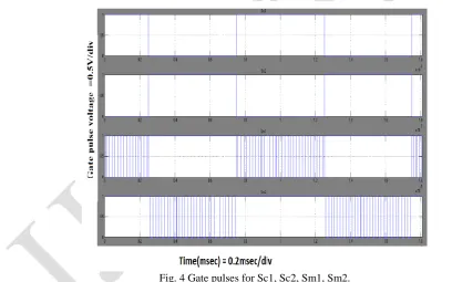
In fig.4 shows the gate pulses for Sc1, Sc2, Sm1, Sm2.When Sc1 is on (1KHZ) Sc2 off and sm1 is operate at 60KHZ.Similiarly when Sc2(1KHZ) is on Sc1 is off Sm2 operate at 60KHZ.
Fig. 4 Gate pulses for Sc1, Sc2, Sm1, Sm2.
10.15662/ijareeie.2014.0308025
Copyright to IJAREEIE www.ijareeie.com 11161
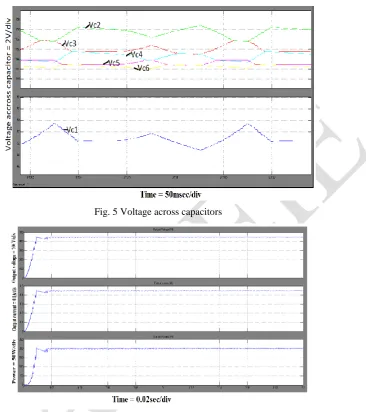
Fig. 5 Voltage across capacitors
Fig .6 Output Wave forms for output voltage (Vo), output current (io), Output Power (Wo)
These are simulated results obtained for the 3-stage Cockcroft-Walton (CW) voltage multiplier. The input voltage for Cockcroft-Walton (CW) generator is 48V, Output voltage is 450V, output current is 0.45Amp, and Output power is 200W. The output voltage range can be increased by adding the number of stages, for every stage we have to connect the two more capacitors and two more diodes.
VI.CONCLUSION
10.15662/ijareeie.2014.0308025
Copyright to IJAREEIE www.ijareeie.com 11162
REFERENCES
[1] B. K. Bose, “Energy, environment, and advances in power electronics,” IEEE Trans. Power Electron., vol. 15, no. 4, pp. 688–701, Jul. 2000. [2] F. Blaabjerg,Z. Chen, and S. B. Kjaer, “Power electronics as efficient z interface in dispersed power generation systems,” IEEE Trans. Power
Electron., vol. 19, no. 5, pp. 1184–1194, Sep. 2004.
[3] Q. Li and P. Wolfs, “A review of the single phase photovoltaic module integrated converter topologies with three different dc link configurations,” IEEE Trans. Power Electron., vol. 23, no. 3, pp. 1320–1333, May 2008.
[4] J. Wang, F. Z. Peng, J. Anderson, A. Joseph, and R. Buffenbarger, “Low cost fuel cell converter system for residential power generation,”
IEEETrans. Power Electron., vol. 19, no. 5, pp. 1315–1322, Sep. 2004.
[5] W. Li and X. He, “Review of nonisolated high-step-up dc/dc converters in photovoltaic grid-connected applications,” IEEE Trans. Ind. Electron., vol. 58, no. 4, pp. 1239–1250, Apr. 2011.
[6] L. S. Yang, T. J. Liang, and J. F. Chen, “Transformer less dc-dc converters with high step-up voltage gain,” IEEE Trans. Ind. Electron., vol. 56, no. 8, pp. 3144–3152, Aug. 2009.