Design and Simulation of Fuzzy Controlled
D-STATCOM to Enhance Power Quality
VADLAMUDI JAGADEESH M-tech Student Scholar
Department of Electrical & Electronics Engineering, Malla Reddy Engineering College, Dhulapally (Post. Via. Kompally);
Rangareddy (Dt); T elangana, India.
V. GANESH KUMAR Associate Professor
Department of Electrical & Electronics Engineering, Malla Reddy Engineering College, Dhulapally (Post. Via. Kompally);
Rangareddy (Dt); T elangana, India.
Abstract-Distribution static compensator (DST AT COM ) is a shunt compensation device that is generally used to solve power quality problems in distribution systems. In an all-electric ship p ower system, power quality issues arise due t o high -energy demand loads such as p ulse loads. In t his p roject a new algorithm to generate reference voltage for a distribution st at ic compensator (DSTATCOM) operating in voltage-control mode. T hree filter capacitors, one for each p hase, are connect ed in p arallel with the DSTATCOM t o eliminat e high -frequency switching components. The voltage across the filter capacitor is controlled by a dead-beat controller t o maint ain t he AC bus voltage. The magnitude of the bus voltage is chosen as nominal value, i.e., 1.0 p.u., while its phase angle is obtained t hrough a feedback loop that maintains the voltage across the DC st orage cap acitors. The proposed scheme ensures that unity power factor (UPF) is achieved at the load terminal during nominal operation, which is not possible in t he t radit ional met hod. Also, t he compensator injects lower currents and, therefore, reduces losses in t he feeder and volt age-source invert er. Nearly UPF is maintained, while regulating voltage at the load terminal, during load change. T he st at e-sp ace model of DST AT COM is incorporated with the deadbeat predictive controller for fast load voltage regulation during voltage disturbances. DSTATCOM to t ackle p ower-qualit y issues by p roviding p ower fact or correction, harmonic elimination, load balancing, and volt age regulation based on the load requirement and simulation result s are p resent ed by using M at lab/Simulink p lat form.
I ndex Terms—Current control mode, power quality (PQ), voltage-control mode, voltage-source inverter.
I. INTRODUCTION
Power Quality (PQ) is the key to successful delivery of quality product and operation of an industry. The increased application of electronic loads and electronic controllers which are sensitive to the quality of power makes serious economic consequences and of revenues loss each year. Poor PQ can cause malfunctioning of equipment performance, harmonics, voltage imbalance, sag and flicker problems, standing waves and resonance – are some of the issues that adversely affect production and its quality leading to huge loss in terms of product, energy and damage to equipment. Thus, it becomes
imperative to be aware of quality of power grid and the deviation of the quality parameters from the norms /standard such as IEEE-519 standard [1] to avoid breakdown or equipment damage.
In present day distribution systems (DS), major power consumption has been in reactive loads. The typical loads may be computer loads, lighting ballasts, small rating adjustable speeds drives (ASD) in air conditioners, fans, refrigerators, pumps and other domestic and commercial appliances are generally behaved as nonlinear loads. These loads draw lagging power-factor currents and therefore give rise to reactive power burden in the DS. Moreover, situation worsens in the presence of unbalanced and non-linear loads, affect the quality of source currents to a large extent. It affects the voltage at point of common coupling (PCC) where the facility is connected. This has adverse effects on the sensitive equipments connected to PCC and may damage the equipment appliances. Excessive reactive power demand increases feeder losses and reduces active power flow capability of the DS, whereas unbalancing affects the operation of transformers and generators [2-3].
controller based five-level CHB multilevel inverter for the current harmonic, voltage flicker and reactive power mitigation of the nonlinear load.
II. PROPOSED CONTROL SCHEME
Circuit diagram of a DSTATCOM-compensated distribution system is shown in Fig.1. It uses a three-phase, four-wire, two-level, neutral-point-clamped VSI. This structure allows independent control to each leg of the VSI [7]. Fig.2 shows the single-phase equivalent representation of Fig.1. Variable is a switching function, and can be either or depending upon switching state. Filter inductance and resistance are and, respectively. Shunt capacitor eliminates high-switching frequency components. First, discrete modeling of the system is presented to obtain a discrete voltage control law, and it is shown that the PCC voltage can be regulated to the desired value with properly chosen parameters of the VSI. Then, a procedure to design VSI parameters is presented. A proportional-integral (PI) controller is used to regulate the dc capacitor voltage at a reference value. Based on instantaneous symmetrical component theory and complex Fourier transform, a reference voltage magnitude generation scheme is proposed that provides the advantages of CCM at nominal load. The overall controller block diagram is shown in Fig. 3 These steps are explained as follows.
Fig.1.Circuit diagram of the DST AT COM-compensated distribution system.
Fig.2 Single-phase equivalent circuit of DST AT COM.
A. System Modeling and Generation of the Voltage-Control Law
The state-space equations for the circuit shown in Fig. 2 are given by
𝑥̇ = Ax + Bz (1)
A=
[
0 𝐶𝑓1𝑐 0
− 1
𝐿𝑓 0 0
−1
𝐿𝑠 0 −
𝑅𝑆
𝐿𝑠]
B=
[
0 −𝐶𝑓1𝑐 0
𝑉𝑑𝑐
𝐿𝑓 0 0
0 0 1
𝐿𝑠]
x=[𝑣𝑓𝑐 𝑖𝑓𝑖 𝑖𝑠]𝑡, z=[𝑢 𝑖𝑓𝑡 𝑣𝑠]𝑡
The general time-domain solution of (1) to compute the state vector x (t) with known initial value x (𝑡0), is given
as follows:
X (t) = X (𝑒𝐴 (𝑡−𝑡0) x (𝑡
0) + ∫ 𝑒𝐴 (𝑡 −𝜏)B z (𝜏) dτ
𝑡
𝑡0 (2)
The equivalent discrete solution of the continuous state is obtained by replacing 𝑡0= k𝑇𝑑and t= (k+1)𝑇𝑑 as follows:
X (k+1) = 𝑒𝐴 𝑇𝑑x (k) + ∫𝑇𝑑 𝑒𝐴(𝑇𝑑+𝑘𝑡𝑑−𝜏)
𝑘𝑇𝑑 B z (τ) dτ (3) (3)
In (3), k and 𝑇𝑑 represent the 𝐾𝑡ℎ sample and sampling
period, respectively. During the consecutive sampling period, the value of z (τ) is held constant, and can be taken as z (k) .After simplification and changing the integration variable, (3) is written as [12]
X (k+1) = 𝑒𝐴 𝑇𝑑x (k) + ∫𝑇𝑑𝑒𝐴𝜆𝐵𝜆
0 B z (K) (4)
x (k+1) = G x (K) + H z (k) (5) Where G and H are sampled matrices, with a sampling
time of 𝑇𝑑. For small sampling time, matrices and are
calculated as follows:
G=[
𝐺11 𝐺12 𝐺13
𝐺21 𝐺22 𝐺23
𝐺31 𝐺32 𝐺33
] (6)
H=[
𝐻11 𝐻12 𝐻13
𝐻21 𝐻22 𝐻23
𝐻31 𝐻32 𝐻33
] = ∫𝑇𝑑𝑒𝐴𝜆𝐵𝜆 0
=∫ ( 𝐼 + 𝐴 𝜆 )𝐵 𝜆0𝑇𝑑 (7) From (6) and (7) 𝐺11= 1 - 𝑇𝑑2/2𝐿𝐹𝑐𝑓𝑐,
𝐺12= 𝑇𝑑/ 𝑐𝑓𝑐- 𝑇𝑑 2
𝑅𝑓/2𝐿𝐹𝑐𝑓𝑐
𝐺13 = 0 ,
𝐻11= 𝑇𝑑2𝑣𝑑𝑐/2𝐿𝐹𝑐𝑓𝑐,
𝐻12= −𝑇𝑑/𝑐𝑓𝑐,
𝐻13= 0. Hence, the capacitor voltage
𝑣𝑓𝑐(𝑘 + 1) = 𝐺11𝑣𝑓𝑐(k) + 𝐺12𝑖𝑓1 +𝐻11 𝑢(𝑘) +
𝐻12 𝑖𝑓1 (𝑘) . (8)
As seen from (8), the terminal voltage can be maintained at a reference value depending upon the VSI parametersvdc, cfc,LF,RF, and sampling timeTd.
Therefore, VSI parameters must be chosen carefully. Let
vt∗ be the reference load terminal voltage. A cost function
J is chosen as follows [8]:
J = [𝑣𝑓𝑐(𝑘 + 1) − 𝑣𝑡∗(𝑘 + 1)2 (9)
The cost function is differentiated with respect to u (k) and its minimum is obtained at
The deadbeat voltage-control law, from (8) and (10), is given as
𝑢𝑡∗(𝑘) =
𝑣𝑡∗(𝑘+1)− 𝐺11𝑣𝑓𝑐(k)− 𝐺12𝑖𝑓1 (𝑘) − 𝐻12 𝑖𝑓𝑡 (𝑘)
𝐻11
(11)
Fig.3 Overall block diagram of the controller to control DST ATCOM in a distribution system.
In (11), vt∗(k + 1) is the future reference voltage which is
unknown. One-step-ahead prediction of this voltage is done using a second-order Lagrange extrapolation formula as follows:
(12) The term vt∗(k + 1) is valid for a wide frequency range
and when substituted in (11), yields to a one-step-ahead deadbeat voltage-control law. Finally ut∗(k), is converted
into the ON/OFF switching command to the corresponding VSI switches using a deadbeat hysteresis controller.
B. Design of VSI Parameters
DSTATCOM regulates terminal voltage satisfactorily, depending upon the properly chosen VSI parameters. The design procedure of these parameters is presented as follows.
Voltage A cros s DC Bus ( 𝒗𝒅𝒄): The dc bus voltage is
taken twice the peak of the phase voltage of the source for
satisfactory performance. Therefore, for a line voltage of 400 V, the dc bus voltage is maintained at 650 V.
DC Capacitance ( 𝑪𝒅𝒄): Values of dc capacitors are
chosen based on a period of sag/swell and change in dc bus voltage during transients. Let the total load rating be S kVA. In the worst case, the load power may vary from minimum to maximum that is, from 0 to S kVA. The compensator needs to exchange real power during transient to maintain the load power demand. This transfer of real power during the transient will result in the deviation of capacitor voltage from its reference value. The voltage continues to decrease until the capacitor voltage controller comes into action. Consider that the voltage controller takes a ρ cycle that is ρT, seconds to act, where T the system is time period. Hence, maximum energy exchange by the compensator during transient will be. This energy will be ρ S T equal to the change in the capacitor stored energy. Therefore
(13) Where and are the reference dc bus voltage and maximum-allowed voltage during transients, respectively. Hence
(14) Here, S=10 kVA, Vdcref=650 V, ρ=1, and or,
Vdcref=0.8VdcrefOR 1.2Vdcref. Using (14), capacitor
values are found to be 2630 and 2152μF. The capacitor value 2600μF is chosen to achieve satisfactory performance during all operating conditions.
Filter Inductance𝑳𝒇 : Filter inductance Lf should provide
reasonably high switching frequency(fmax) and a
sufficient rate of change of current such that VSI currents follow desired currents. The following equation represents inductor dynamics:
(15) The inductance Lf is designed to provide good tracking
performance at a maximum switching frequency(fmax)
which is achieved at the zero of the source voltage in the hysteresis controller. Neglecting Rf, Lf is given by
(16) Where 2hc is the ripple in the current. With fmax = 10
kHz and hc = 0.75 A (5% of rated current), the value Lf
Shunt Capacitor (𝑪𝒇𝒄): The shunt capacitor should not
resonate with feeder inductance at the fundamental frequency (ω0). Capacitance, at which resonance will occur, is given as
(17) For proper operation, Cfc must be chosen very small
compared to Cfcr . Here, a value of 5μF is chosen which
provides an impedance of 637 ohm atω0. This does not
allow the capacitor to draw significant fundamental reactive current.
III. CONTROLLER FOR DC BUS CAPACITOR VOLTAGE
Average real power balance at the PCC will be
(18) Where Ppcc, P1avg, and Ploss are the average PCC power,
load power, and losses in the VSI, respectively. The power available at the PCC, which is taken from the source, depends upon the angle between source and PCC voltages, that is, load angle. Hence δ must be maintained
Ppccconstant to keep constant. The voltage of the dc bus
of DSTATCOM can be maintained at its reference value by taking inverter losses Ploss from the source. If the
capacitor voltage is regulated to a constant reference valuePloss, is a constant value. Consequently, δ is also a
constant value. Thus, it is evident that dc-link voltage can be regulated by generating a suitable value δ of .This δ includes the effect of losses in the VSI and, therefore, it takes care of Plossthe term in its action. To calculate load
angle δ, the averaged dc-link voltage (Vdc1+ Vdc2) is
compared with a reference voltage, and error is passed through a PI controller. The output of the PI controller, which is load angle δ, is given as follows:
(19) Where evdc = 2Vdcref−(Vdc1+Vdc2) is the voltage error.
Terms Kpδ and Kiδ are proportional and integral gains,
respectively. δ must lie between 0 to 900 for the power
flow from the source to PCC. Hence, controller gains must be chosen carefully.
IV. PROPOSED METHOD TO GENERATE REFERENCE TERMINAL VOLTAGES
Reference terminal voltages are generated such that, at nominal load, all advantages of CCM operation are
achieved while DSTATCOM is operating in VCM. Hence, the DSTATCOM will inject reactive and harmonic components of load current. To achieve this, first the fundamental positive-sequence component of load currents is computed. Then, it is assumed that these currents come from the source and considered as reference source currents at nominal load. With these source currents and for UPF at the PCC, the magnitude of the PCC voltage is calculated. Let three-phase load currentsila,ilb, and ilcbe represented by the following
equations:
(20) Where j= a, b, c represent three phases n, is the harmonic number, and m is the maximum harmonic orderϕlan represents the phase angle of the th harmonic with respect to reference in phase-α and is similar to other phases. Using instantaneous symmetrical component theory, instantaneous zero-sequenceila0(t),
positive-sequenceila+(t), and negative-sequence currentila−(t),
components are calculated as follows:
(21) Where α is a complex operator and defined by ej2∏⁄3.
The fundamental positive-sequence component of load current I̅la1+ , calculated by finding the complex Fourier coeficient, is expressed as follows:
(22)
𝐼̅𝑙𝑎1+ Is a complex quantity, contains magnitude and phase
angle information, and can be expressed in phasor form as follows:
(23) Hence, the instantaneous fundamental positive-sequence component of load current in phase-a, 𝐼̅𝑙𝑎1+ is expressed as
(24) The fundamental positive-sequence component of load currents must be supplied by the source at nominal load. Hence, it will be treated as reference source currents. For UPF at nominal operation, the nominal load angle 𝛿0 is
used. By knowing 𝐼̅𝑙𝑎1+ fundamental positive-sequence
providing a phase displacement of −2∏⁄3and2∏⁄3, respectively, and are given as
(25) When reference source currents derived in (25) are supplied by the source, three-phase terminal voltages can be computed using the following equations:
(26) Let the rms value of reference terminal and source voltages be Vt∗ and V, respectively. For UPF, the source
current and terminal voltage will be in phase. However, to obtain the expression of V∗independent of δ
0 , we assume
the PCC voltage as a reference phasor for the time-being. Hence, phase-α quantities, by considering UPF at the PCC, will be
(27) Substituting (27) into (26), the phasor equation will be
(28) Simplifying the above equation
(29) Equating real and imaginary parts of both sides of (29), the following equation is obtained:
(30) To remove 𝛿0 from (30), both sides are squared and added
to obtain the following:
(31) After rearranging (31), the expression for reference load voltage magnitude will be
(32) Finally, using 𝑣𝑡∗ from (32), the load angle from (19), and
the phase-α source voltage as reference, three-phase reference terminal voltages are given as
(33) V.MATLAB/SIMULINK RESULTS
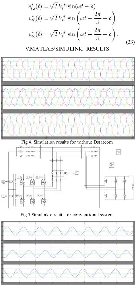
Fig.4. Simulation results for without Dstatcom
Fig.5.Simulink circuit for conventional system
Fig.7. voltage at the dc bus
Fig.8.Simulink circuit for proposed system with PI controller
Fig. 9. T erminal voltages and source currents using the proposed method using PI controller.(a) Phase a (b) Phase b. (c) Phase c.
Fig.10. simulation results for compensation currents
Fig. 11. Load reactive power , compensator reactive power, and
reactive power at PCC for Proposed method with pi controller
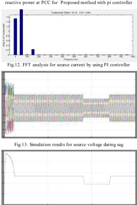
Fig.12. FFT analysis for source current by using PI controller
Fig.13. Simulation results for source voltage during sag
Fig.14. simulation result for RMS value of source voltage during sag
Fig 15. Simulation results for dc link voltage
Fig.17. simulation results for compensation current of statcom
Fig. 18. T erminal voltages and source currents using the proposed method using fuzzy controller.(a) Phase a (b) Phase b. (c) Phase c.
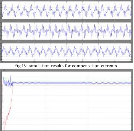
Fig.19. simulation results for compensation currents
Fig. 20. Load reactive power , compensator reactive power, and reactive power at PCC for Proposed method with fuzzy controller
Fig.21. FFT analysis for source current by using fuzzy controller
VI.CONCLUSION
In this paper, a control algorithm has been proposed for the generation of reference load voltage for a voltage-controlled DSTATCOM. The performance of the proposed scheme is compared with the traditional voltage-controlled DSTATCOM. The proposed method provides the following advantages:
1) At nominal load, the compensator injects reactive and harmonic components of load currents, resulting in UPF; 2) Nearly UPF is maintained for a load change;
3) Fast voltage regulation has been achieved during voltage disturbances.
4) Losses in the VSI and feeder are reduced considerably, and have higher sag supporting capability with the same VSI rating compared to the traditional scheme.
REFERENCES
[1] M. Bollen, Understanding Power Quality Problems. Piscataway, NJ, USA: IEEE, 2000, ch. 1, pp. 1–35.
[2] H. Fujita and H. Akagi, “Voltage-regulation performance of a shunt active filter intended for installation on a power distribution system,” IEEE T rans. Power Electron., vol. 22, no. 3, pp. 1046–1053, May 2007. [3] A. Ghosh and G. Ledwich, “Load compensating DST AT COM in weak ac systems, ”IEEE Trans. Power Del., vol. 18, no. 4, pp. 1302– 1309, Oct. 2003.
[4] A. Elnady and M. Salama, “Unified approach for mitigating voltage sag and voltage flicker using the DST AT COM,” IEEE T rans. Power Del., vol. 20, no. 2, pt. 1, pp. 992–1000, Apr. 2005.
[5] S.Rahmani, A.Hamadi, andK.Al-Haddad,“ALyapunov-function based control for a three-phase shunt hybrid active filter, ”IEEE T rans. Ind. Electron., vol. 59, no. 3, pp. 1418–1429, Mar. 2012. [6] M. K. Mishra and K. Karthikeyan, “A fast -acting dc-link voltage controller for three-phase DST ATCOM to compensate ac and dc loads,” IEEE T rans. Power Del., vol. 24, no. 4, pp. 2291–2299, Oct. 2009. [7] M. K. Mishra, A. Ghosh, A. Joshi, and H. M. Suryawanshi, “A novel method of load compensation under unbalanced and distorted voltages,”IEEE Trans. Power Del., vol. 22, no. 1, pp. 288 –295, Jan. 2007.
[8] M.K.Mishra, A.Ghosh, and A .Joshi,“ Operation of a DST AT COM in voltage control mode,”IEEE Trans. Power Del.,vol.18,no.1,pp. 258– 264, Jan. 2003.
[9] A. Jain, K. Joshi, A. Behal, and N. Mohan, “Voltage regulation with ST AT COMs: Modeling, control and results, ”IEEE T rans. Power Del., vol. 21, no. 2, pp. 726–735, Apr. 2006.
[11] P. Mitra and G. Venayagamoorthy, “An adaptive control strategy for DST ATCOM applications in an electric ship power system,”IEEE T rans. Power Electron., vol. 25, no. 1, pp. 95–104, Jan. 2010. [12] A. Yazdani, M. Crow, and J. Guo, “An improved nonlinear ST AT COM control for electric arc furnace voltage flicker mitigation,”IEEE T rans. Power Del., vol. 24, no. 4, pp. 2284–2290, Oct. 2009.