Broadband Vertical Transitions Between Double-Sided Parallel-Strip
Line and Coplanar Waveguide
Nelson K. Jacob, Lindo A. Ouseph, Chandroth K. Aanandan,
Mohanan Pezholil, and Kesavath Vasudevan*
Abstract—A pair of broadband double-sided parallel-strip line (DSPSL) to coplanar waveguide (CPW)
vertical transitions are presented. The transitions are composed of CPW open end with connected grounds forming two strips of the DSPSL with single via connection. The connected grounds of CPW, which forms top strip of the DSPSL are of two different shapes resulting in two transitions (Types 1 & 2). Simulated results for the back-to-back transitions, using the multilayer solver of CST Microwave Studio, show good agreement with the measured ones.
1. INTRODUCTION
Vertical transitions are crucial components in double-layer microwave circuits to avoid the use of crossovers. DSPSL, also known as broadside coupled stripline (BCS), is a balanced transmission line, with wide range of characterictic impedances, differential signalling and simple transition structures [1]. However, no vertical transitions between DSPSL and CPW have been reported yet. Back to back vertical transitions of DSPSL in direct and inverted forms are capable of achieving signal/phase inversion, resulting in microwave applications such as mixers and ring couplers. Traditionally, vertical transitions will use either low-pass natured via connection or band-pass natured slot/cavity coupling.
Due to the wide popularity of CPW probe pads, various wideband transitions between CPW and DSPSL have been proposed in recent years [2–5]. Furthermore, majority of them are built on high dielectric-constant substrates for attaining low characteristic impedances thereby easy matching to 50 Ω lines. However, they are suitable for circuit design instead, and using such transitions to feed antennas will degrade the antenna performance [4]. The optimizations of planar transitions using different techniques have already been reported [10–13].
In this paper, a vertical broadband 50 Ω DSPSL to 50 Ω CPW transition is proposed for the first time. A simplified equivalent circuit revealing the basic low pass nature is introduced. The back-to-back transitions on a 1.524 mm thickness Rogers RO4003C substrate yield return and isolation losses better than 14.5 dB and 2.5 dB respectively, from DC to 11.5 GHz, and for 1.6 mm thickness FR4 substrate, the return and insertion losses better than 15.0 dB and 4.0 dB respectively, from DC to 11.0 GHz. It has an optimized structure with a single via, which can be easily fabricated.
2. DOUBLE-SIDED PARALLEL-STRIP LINE
The DSPSL is two identical metal strips separated by a dielectric slab. It possesses a wide range of characteristic impedance, which validates the feasibility in constructing new high performance
Received 26 March 2018, Accepted 25 April 2018, Scheduled 4 May 2018
* Corresponding author: Kesavath Vasudevan ([email protected]).
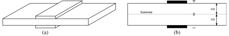
microwave circuits and integrating with other microwave circuits/components without any impedance transformer. As per image theory, the middle plane of the dielectric slab is a virtual ground plane to form identical microstrip lines with half the substrate thickness (h/2) as shown in Fig. 1. The relationship of the characteristic impedances between them is
(Z0)dspsl= 2∗(Z0)microstrip
For unbalanced transmission lines such as microstrip line and CPW, very high impedance is not available due to fabrication limitation. On the other hand, for the CPS and slot line, very low impedance is not available due to the small capacitance between the two strips. Like microstrip line, strip width is also a key factor in controlling the characteristic impedance of the DSPSL. However, offset top and bottom lines of the DSPSL result in higher impedances. According to [1, 7–9], it finds applications in filters, rat-race hybrid couplers, power dividers and antenna feeds, etc. for frequencies ranging up to 30 GHz.
0 Substrate
(a) (b)
h/2
h/2
Figure 1. Double-sided parallel-strip line, (a) three dimensional view, (b) cross sectional view.
3. TRANSITION DESIGN
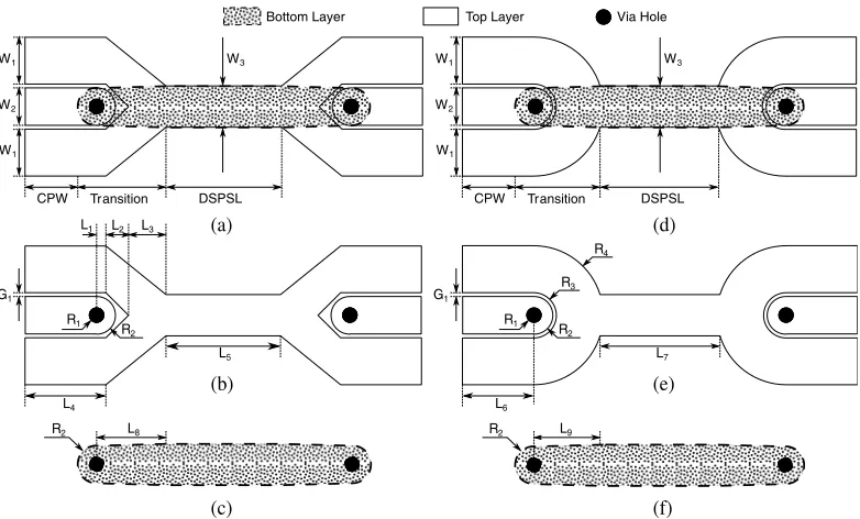
Geometrical layouts of the transitions between 50 Ω CPW and 50 Ω DSPSL are shown in Fig. 2. To design a good transition between transmission lines, gradual change in electromagnetic (EM) fields and impedance matching are required. Since realization of different characteristic impedance values of DSPSL is comparatively easy, in these designs only smooth transition of EM field from CPW mode to DSPSL mode is considered to avoid any abrupt discontinuities. However, to obtain field matching, parallel electric field of CPW is to be rotated 90◦ to become the vertical electric field of DSPSL. The equal magnitude currents flowing in the DSPSL conductors show 180◦ out of phase nature. On the other hand, due to the presence of two ground lines in CPW, the center strip carries doubled value of their individual current magnitude.
The currents of top strip line of DSPSL and ground lines of CPW have identical directions in the proposed vertical transition structure. The top strip of DSPSL is formed from the connected grounds of CPW which takes a ‘v’-shape in type 1 and semi-ring shape in type 2 transitions, respectively. The center conductor of CPW has to be connected to the bottom strip of DSPSL, and two methods can be used for this. One uses EM coupling between them, and the other is a single via connecting them directly. We choose the latter for our design because of enhanced bandwidth (zero frequency onwards), simple structure and compact size, since EM coupling requires comparatively large structures and low bandwidth.
Multilayer solver (Frequency domain) of CST Microwave Studio (3D planar electromagnetic solver based on MoM) is used for the parametric studies and optimization. The transitions are printed on two similar substrates, Roger’s RO4003C (r = 3.55 & h = 1.524 mm) and FR4 (r = 4.3 & h= 1.6 mm). The dimensions of 50 Ω CPW are determined by CST Microwave Studio utility with the center strip width W1 = 4.0 mm and gap width G1 = 0.35 mm for both cases. Using image theory, the strip width of the 50 Ω DSPSL can be calculated asW2= 4.4 mm.
3.1. Type 1
Bottom Layer Top Layer Via Hole
CPW Transition DSPSL W1
W2
W1
(a) (d)
(b) (e)
(c) (f)
L4
R1
R2
R1
R2
G1 G1
R3
R4
R2 R2
L1
L8 L9
W1
W2
W1
CPW Transition DSPSL
L2 L3
L5
L6
L7
W3 W3
Figure 2. Configuration of the back-to-back transitions (Type 1 & Type 2): (a) schematic layout
(Type 1), (b) top view (Type 1), (c) bottom view (Type 1), (d) schematic layout (Type 2), (e) top view (Type 2), and (f) bottom view (Type 2). (W1 = 5 mm, W2 = 4 mm, W3 = 4.4 mm, G1 = 0.35 mm,
L1 = 1 mm, L2 = 2.4 mm, L3 = 4 mm, L4 = 8.6 mm, L5 = 6.24 mm, L6 = 7.6 mm, L7 = 6.24 mm,
L8 = 7.4 mm,L9 = 7.4 mm,R1 = 0.75 mm,R2= 2 mm, R3 = 2.35 mm,R4= 7.35 mm).
The CPW center strip and DSPSL bottom metal are circularly terminated to form via pads with radius equal to half their width (R2 = 2 mm). In Fig. 2(c) after via connection (R1 = 0.75 mm), the width of the bottom metal strip is gradually increased for a length (L8 = 7.4 mm), to match the width of DSPSL (W3 = 4.4 mm).
3.2. Type 2
As shown in Fig. 2(e), ground conductors are circularly tapered with inner radius (R3 = 2.35 mm) and outer radius (R4 = 7.35 mm) to form the top metal of DSPSL. The rest of the design is exactly the same as Type 1. The total transition length is (L9= 7.4 mm).
4. EQUIVALENT CIRCUIT
The electric field at the open circuit between connected ground conductor and terminated center conductor results in capacitive reactance [6]. A via is used in series with the signal line whenever we wish a signal to change layers in a two-sided or multilayer circuit. The lower frequency response of the via tends to look capacitive. At higher frequencies, the upper and lower pads of the via remain capacitive, but the cylindrical part will become more inductive in nature. An approximate equivalent circuit which excludes coupling effects, for determining the response of the transition, is given in Fig. 3. The equivalent circuit behaves as a Π network LC low-pass filter which has capacitive components to ground and inductive series components. Transitions involving multiple vias will have the cascading effect of several low-pass filter sections which will provide greater roll off.
5. MEASURED AND SIMULATED RESULTS
CPW
DSPSL
CVia
LVia
COpen CVia
Transition
(Type 1 )
(Type 2 ) CPW
(Type 1 )
(Type 2 )
CVia LVia CVia (a) (b) (c) COpen
Figure 3. Simplified equivalent circuit: (a) equivalent cicuit of CPW with connected grounds, (b)
equivalent cicuit of via (Lumped), (c) complete equivalent cicuit of the transitions (Type 1 & Type 2).
(a) (c)
(c)
Top View Bottom View Top View Bottom View
0 2 4 6 8 10 12 14
-40 -35 -30 -25 -20 -15 -10 -5 0
Scattering Parameters (dB)
Frequency (GHz)
S11 (Measured) S11 (Simulation) S21 (Measured) S21 (Simulation)
0 2 4 6 8 10 12 14
-40 -35 -30 -25 -20 -15 -10 -5 0
Scattering Parameters (dB)
Frequency (GHz)
S11 (Measured) S11 (Simulation) S21 (Measured) S21 (Simulation)
0 2 4 6 8 10 12 14
-40 -35 -30 -25 -20 -15 -10 -5 0
Scattering Parameters (dB)
Frequency (GHz)
S11 (Measured) S11 (Simulation) S21 (Measured) S21 (Simulation)
0 2 4 6 8 10 12 14
-40 -35 -30 -25 -20 -15 -10 -5 0
Scattering Parameters (dB)
Frequency (GHz)
S11 (Measured) S11 (Simulation) S21 (Measured) S21 (Simulation) Top View Bottom View Top View Bottom View
(d)
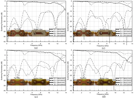
Figure 4. Simulated and measured scattering parameters of the back-to-back transitions, (a) Type 1
Table 1. Measured losses of the back-to-back transitions.
Type Substrate Bandwidth (GHz) Insertion loss (dB) Return loss (dB)
1 Rogers RO4003C 0.0–12.1 ≤2.5 ≥9.0
1 FR4 0.0–11.0 ≤4.0 ≥15.0
2 Rogers RO4003C 0.0–11.5 ≤2.5 ≥14.5
2 FR4 0.0–10.7 ≤4.0 ≥13.4
network analyzer respectively, which are illustrated in Fig. 4 and show good match. The actual photographs of top and bottom views of all transitions are also included in the same figure. Table 1 shows the measured insertion and return losses of the transitions for different substrates.
From the measured group delays, average delay deviation for 30 kHz to 14 GHz is only about 0.021 ns (Type 1 — Rogers RO4003C), 0.014 ns (Type 2 — Rogers RO4003C), 0.016 ns (Type 1 — FR4) and 0.020 ns (Type 2 — FR4) which are relatively small, indicating good transmission phase linearity of the transitions, as shown in Fig. 5.
(a) (b)
0 2 4 6 8 10 12 14
0.1 0.2 0.3 0.4 0.5 0.6 0.7
Delay (ns)
Frequency (GHz)
Rogers RO4003C FR4
0 2 4 6 8 10 12 14
0.1 0.2 0.3 0.4 0.5 0.6 0.7
Delay (ns)
Frequency (GHz)
Rogers RO4003C FR4
Figure 5. Measured group delays of the back-to-back transitions, (a) Type 1, (b) Type 2.
The insertion loss associated with a single transition, ILT ransition, can be calculated as
ILT ransition= (ILT otal−LCP W −LDSP SL−LSM A)/2
where, ILT otal is the total measured insertion loss; LCP W and LDSP SL are the insertion losses of the CPW and DSPSL lines respectively; LSM A is the insertion loss of SMA connectors. According to [1, 4], the transmission losses of DSPSL and CPW sections are about 0.03 dB/mm and 0.04 dB/mm, respectively, and insertion loss of a single SMA connector is around 0.09 dB. Therefore, maxima in band insertion loss for a single transition are approximately 0.76 dB and 1.51 dB for the substrates Rogers RO4003C and FR4, respectively.
6. CONCLUSION
ACKNOWLEDGMENT
This work has been supported by Council of Scientific & Industrial Research (CSIR), Government of India.
REFERENCES
1. Kim, S. G. and K. Chang, “Ultrawide-band transitions and new microwave components using double-sided parallel-strip lines,”IEEE Transactions on Microwave Theory and Techniques, Vol. 52, No. 9, 2148–2152, 2004.
2. Chen, J. X., J. L. Li, and Q. Xue, “Novel via-less double-sided parallel-strip line to coplanar waveguide transition,”Microwave and Optical Technology Letters, Vol. 48, No. 9, 1717–1718, 2006. 3. Zhang, X. Y., J. X. Chen, and Q. Xue, “Broadband transition between double-sided parallel-strip line and coplanar waveguide,”IEEE Microwave and Wireless Components Letters, Vol. 17, No. 2, 103–105, 2007.
4. Lu, W. J., H. Tong, Y. M. Bo, and H. B. Zhu, “Design and study of enhanced wideband transition between coplanar waveguide and broadside coupled stripline,” IET Microwaves, Antennas and Propagation, Vol. 7, No. 9, 715–721, 2013.
5. Kim, Y. G. and K. W. Kim, “Design of an ultra-wideband transition from double-sided parallel stripline to coplanar waveguide,” International Journal of Antennas and Propagation, Article ID 921859, 8 pages, doi:10.1155/2013/921859, 2013.
6. Simons, R. A., Coplanar Waveguide Circuits, Components and Systems, IEEE Press, Wiley, 2001. 7. Sun, C.-G. and J.-L. Li, “Design of planar multi-way differential power division network using
double-sided parallel stripline,”Electron Letters, Vol. 53, No. 20, 1364–1366, 2017.
8. Bo, L. W., X. Q. Lin, and F. Cheng, “Electric split-ring resonator based on double-sided parallel-strip line,” IEEE Antennas and Wireless Propagation Letters, Vol. 12, 69–71, 2013.
9. Zhong, Z. W., Y. X. Li, Z. X. Liang, and Y. L. Long, “Biplanar monopole with DSPSL feed and coupling line for broadband mobile phone,” IEEE Antennas and Wireless Propagation Letters, Vol. 11, 1326–1329, 2012.
10. Carro, P. L. and J. Mingo, “Analysis and synthesis of double-sided parallel-strip transitions,”IEEE Transactions on Microwave Theory and Techniques, Vol. 58, No. 2, 372–380, 2010.
11. Kumar, B. P. and G. R. Branner, “Optimized design of unique miniaturized planar baluns for wireless applications,” IEEE Microwave Wireless Components Letters, Vol. 13, No. 3, 134–136, 2003.
12. Staiculescu, D., N. Bushyager, A. Obatoyinbo, L. J. Martin, and M. M. Tentzeris, “Design and optimization of 3-D compact stripline and microstrip Bluetooth/WLAN balun architectures using the design of experiments technique,” IEEE Transactions on Antennas and Propagation, Vol. 53, No. 5, 1805–1812, 2005.