98 | P a g e
www.ijarse.com
DESIGN AND IMPLEMENTATION OF OPTIMIZED 4:1
MUX USING ADIABATIC TECHNIQUE
1
Dikshant Kamboj,
2Arvind Kumar,
3Vijay Kumar
1
M.Tech (Microelectronics),
2,3Assistant Professor,
University Institute of Engineering and Technology, Panjab University, Chandigarh(India)
ABSTRACT
A multiplexer is the integral part of the any digital circuit and one of the most utilized circuits. A variety
of applications a multiplexer has, where a multiplexer can be implemented for e.g. in Full Adder,
Arithmetic Logic Unit (ALU), Digital Compressor etc. In this paper authors have proposed a 4:1
multiplexer using PFAL and ECRL adiabatic logic design technique and compared with the Conventional
CMOS Multiplexer. The power dissipation of the proposed circuits, is compared to a Conventional
CMOS Multiplexer with respect to the clock frequency, Load Capacitance and Supply Voltage. The
schematic design and simulation has been carried out in the Tanner V.13 in 180nm CMOS Technology.
The result shows the great improvement in the power dissipation result. The result also shows the
considerable reduction in the area of the proposed 4:1 Multiplexer
.
Keywords: Adiabatic, Multiplexer, PFAL, ECRL, Low Power, CMOS
I INTRODUCTION
Electronic device sizes are getting reduced day by day. As the size of the battery operated device like PDAs, Laptop, Mobile phones etc become quite small. As a result, size the battery also reduced in the same proportion making the device lighter. But on the other hand, the efficiency of the battery decreased and drained quickly. Battery efficiency can be enhanced either by making the size of the battery bigger, but it makes the device bulkier or by designing the circuit which consumes low power. The CMOS circuit has very low power consumption, but a major power dissipating component of the CMOS circuit is the dynamic power. In the CMOS circuit, during the one of the
Supply voltage, during the transition 0 to , energy has been drawn up from the DC power supply. The half
of the power get dissipated across the Pull-Up network and only energy stored at the output load. During the
power supply transition from to 0, the stored energy at the output load gets dissipated to ground through
99 | P a g e
www.ijarse.com
lower limit of power dissipation for the CMOS circuit. But there is another approach through which the power dissipation can be reduced from the theoretical lower limit. The technique is called Adiabatic Technique.[1]
Adiabatic Technique: The word Adiabatic is a Greek term which means “No exchange of heat”. The adiabatic circuit is also called the energy reversible circuit. Unlike the CMOS, the adiabatic circuit has lower dynamic power dissipation. The two key rule by which adiabatic circuits tries to conserve the energy are
a. Never turn on a transistor when there is a voltage potential between source and drain. b. Never turn off a transistor when current is flowing through it. [1][2]
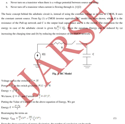
The basic concept behind the adiabatic circuit is, instead of using the constant voltage as in case of CMOS, It uses the constant current source. From fig (1) a CMOS inverter equivalent RC model has been shown, where R is the resistance of the Pull-up network and C is the output load capacitance and S is the switch. The expression for the
energy in case of the adiabatic circuit is given by . From the equation, Energy can be reduced by (a)
increasing the charging time and (b) by reducing the resistance of the PMOS network.
R
I(t)
C
Fig. 1: RC Model
Voltage across the switch is
Power in the switch given by:
Energy
We know, and Current .
Putting the Value of Current I in the above equation of Energy, We get
Energy
Rearranging the terms an
Energy = (1)
100 | P a g e
www.ijarse.com
a. The Energy dissipation is small as compare to the conventional CMOS, by increasing the T>>RC. In other words, Energy dissipation make small by increasing the charging time.
b.
From the equation, the energy dissipation is proportional to the resistance R. On reducing the internal on resistance of the PMOS network Power can be scale down from the lower limitprescribe in case of conventional CMOS.[1, 2
].
II ADIABATIC LOGIC FAMILY ECRL & PFAL
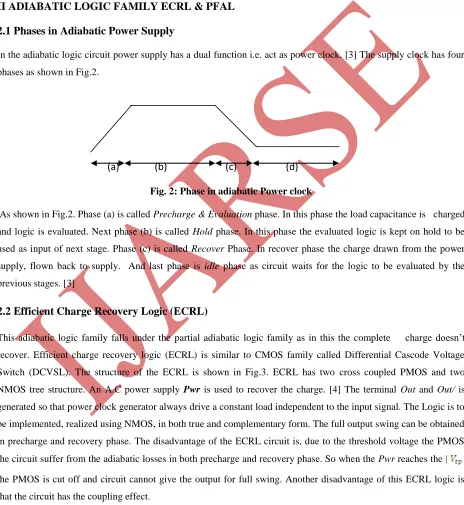
2.1 Phases in Adiabatic Power Supply
In the adiabatic logic circuit power supply has a dual function i.e. act as power clock. [3] The supply clock has four
phases as shown in Fig.2.
(a)
(b)
(c)
(d)
Fig. 2: Phase in adiabatic Power clock
As shown in Fig.2. Phase (a) is called Precharge & Evaluation phase. In this phase the load capacitance is charged and logic is evaluated. Next phase (b) is called Hold phase. In this phase the evaluated logic is kept on hold to be used as input of next stage. Phase (c) is called Recover Phase. In recover phase the charge drawn from the power supply, flown back to supply. And last phase is idle phase as circuit waits for the logic to be evaluated by the previous stages. [3]
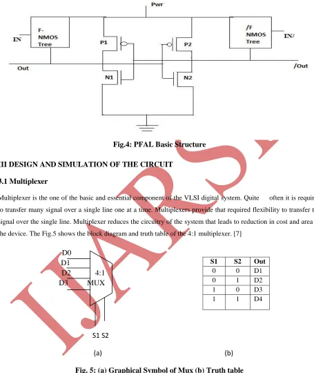
2.2 Efficient Charge Recovery Logic (ECRL)
This adiabatic logic family falls under the partial adiabatic logic family as in this the complete charge doesn’t recover. Efficient charge recovery logic (ECRL) is similar to CMOS family called Differential Cascode Voltage Switch (DCVSL). The structure of the ECRL is shown in Fig.3. ECRL has two cross coupled PMOS and two NMOS tree structure. An A.C power supply Pwr is used to recover the charge. [4] The terminal Out and Out/ is generated so that power clock generator always drive a constant load independent to the input signal. The Logic is to be implemented, realized using NMOS, in both true and complementary form. The full output swing can be obtained in precharge and recovery phase. The disadvantage of the ECRL circuit is, due to the threshold voltage the PMOS
the circuit suffer from the adiabatic losses in both precharge and recovery phase. So when the Pwr reaches the | |
101 | P a g e
www.ijarse.com
Fig.3: ECRL Basic Structure
To understand the circuit operation,
a. Assume the in is high then in/ will be at low level. When the pwr rises from 0 to , in turns on the
F- NMOS tree functional box and Out remain at the zero level. /Out follows the power clock through P1 and rises to. As value reaches to , the Out holds the valid logic level and. The value is
maintained during HOLD phase and can be used as the input of the next stage.
b. During the transition from to 0, the energy is recovered through the path /out and charge
recovered back to Pwr. From this, it can be observed that Pwr is used as power clock and power supply.[5]
2.3 Positive Feedback Adiabatic Logic Circuit (PFAL)
102 | P a g e
www.ijarse.com
Fig.4: PFAL Basic Structure
III DESIGN AND SIMULATION OF THE CIRCUIT
3.1 Multiplexer
Multiplexer is the one of the basic and essential component of the VLSI digital system. Quite often it is required to transfer many signal over a single line one at a time. Multiplexers provide that required flexibility to transfer the signal over the single line. Multiplexer reduces the circuitry of the system that leads to reduction in cost and area of the device. The Fig.5 shows the block diagram and truth table of the 4:1 multiplexer. [7]
D0
D1
D2
4:1
D3 MUX
S1 S2
(a)
(b)
Fig. 5: (a) Graphical Symbol of Mux (b) Truth table
The D0, D1, D2&D3 are the Data Lines and S1&S2 are the select lines. Here is equation of multiplexer.
(2)
S1 S2 Out
103 | P a g e
www.ijarse.com
3.2
Conventional CMOS 4:1 Multiplexer
The transistor level architecture of the Conventional 4:1 Multiplexer is shown in Fig.6. The multiplexer contain 44 transistors. As the transistor counts are high, it leads to increase in the area and power dissipation
Fig.6: Transistor level 4:1 Mux Circuit
3.3 Low Power ECRL and PFAL Multiplexer
The proposed design using adiabatic technique ECRL and PFAL have considerable low power consumption and area as compared to the conventional CMOS multiplexer
104 | P a g e
www.ijarse.com
The Output Waveform of the 4:1 PFAL multiplexer
Fig.8: The PFAL 4:1 MUX Simulation Waveform
The 4:1 MUX using ECRL adiabatic, the proposed circuit is shown in Fig. 9
105 | P a g e
www.ijarse.com
The simulation result of the 4:1 Multiplexer using ECRL is shown in Fig.10
Fig.10: Simulation waveform of 4:1 ECRL Mux
IV IMPACT OF PAMATERIC VARIATION ON POWER CONSUMPTION
The power consumption in adiabatic circuit depends upon the parameter variation. The analysis of the impact in variation in parameter on the power consumption carried out of two logic family with respect to CMOS logic circuit. The design and Simulation of the circuit has been done using TANNER EDA tool by using the 180nm TSMC CMOS technology. The W/L ratio for the PMOS and NMOS are 810/180 and 360/180 respectively.
4.1 Power Vs Clock Frequency
106 | P a g e
www.ijarse.com
Fig. 11 Average Power Vs Clock Frequency at Supply Voltage 1.4v and Load Capacitance 10fF
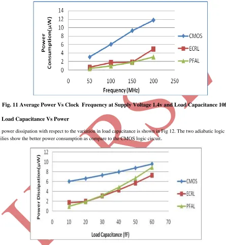
4.2 Load Capacitance Vs Power
The power dissipation with respect to the variation in load capacitance is shown in Fig 12. The two adiabatic logic families show the better power consumption as compare to the CMOS logic circuit
.
Fig.12 Average Power versus Load Capacitance at Supply Voltage1.4V and Clock Frequency
100MHz
4.3 Supply Voltage Vs Power
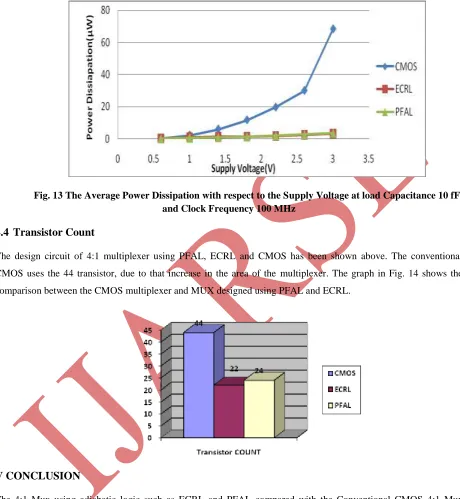
The variation in Supply voltage and corresponding power dissipation is shown in the 13. The CMOS 4:1
107 | P a g e
www.ijarse.com
Fig. 13 The Average Power Dissipation with respect to the Supply Voltage at load Capacitance 10 fF and Clock Frequency 100 MHz
4.4 Transistor Count
The design circuit of 4:1 multiplexer using PFAL, ECRL and CMOS has been shown above. The conventional CMOS uses the 44 transistor, due to that increase in the area of the multiplexer. The graph in Fig. 14 shows the comparison between the CMOS multiplexer and MUX designed using PFAL and ECRL.
V CONCLUSION
108 | P a g e
www.ijarse.com
REFERENCES
[1] William C. Athas, Lars “J.” Svensson, J G Koller, Nestoras Tzartzanis and E. Chou “Low Power Digital system
based on Adiabatic-Switching Principles.” IEEE Trans VLSI systems, Vol. 2, pp. 398-407, Dec 1994
[2] A.P. CHANDRAKASAN AND R. W. BRODERSEN, Low-power CMOS digital design, Kluwer Academic, Norwell, Ma, 1995.
[3] B.VOSS AND M.GLESNER,“A Low Power Sinusoidal Clock,” In Proc. of the International Symposium on
Circuits and Systems, ISCAS 2001.
[4] Y. MOON AND D. K. JEONG, “An Efficient Charge Recovery Logic Circuit,” IEEE JSSC, Vol. 31, No. 04, pp. 514-522, April 1996.
[5] Arun Kumar, Manoj Sharma. “Design and analysis of Mux using Adiabatic ECRL and PFAL” ICCAI , pp. 1341-1345, 2013
[6] A.BLOTTI AND R. SALETTI, “Ultralow- Power Adiabatic Circuit Semi-Custom Design,” IEEE Transactions
on VLSI Systems, vol.12, no. 11, pp. 1248-1253, November 2004.
[7] Meenakshi Mishra, Shyam Akashe, “High Performance, Low power 200Gb/s 4:1 MUX with TGL in 45nm
Technology” Springer, 2013