52 |
P a g e
IMPLEMENTATION OF HIGH SPEED LOW POWER
VEDIC MULTIPLIER USING REVERSIBLE LOGIC
Manoj Kumar.K
1, Dr Meghana Kulkarni
21
PG Scholar,
2Associate Professor
Dept of PG studies, VTU-Belagavi, Karnataka,(India)
ABSTRACT
Multiplication is an operation much needed in Digital Signal processing for various applications. Here we present a high speed Vedic Multiplier which is efficient in terms of speed, making use of Urdhva Tiryagbhyam, a sutra for multiplication from vedic math’s. It is a simple architecture coupled with increased speed forms an unparalleled combination for serving any complex multiplication computation. Tagged with these highlights, power dissipation can be reduced by implementing this with reversible logic. Power dissipation is another important constraint in an embedded system which cannot be neglected. The Reversible Logic has received great attention in the past recent years due to its ability in reducing the power dissipation, which is the major concern in Digital Designing.
Keywords: Vedic Multiplier, Urdhva Tiryakbhayam Sutra, Reversible Logic, Xilinx ISE 14.7
I. INTRODUCTION
The speed of a processor greatly depends on performance of its multiplier’s. This in turn increases the demand for
high speed multipliers, at the same time keeping in mind low area and moderate power consumption. Over the past
few decades, several new architectures of multipliers have been designed and explored. Even though the Booth’s and modified Booth’s algorithm is very popular today in VLSI design it has its own intrinsic disadvantage that it
involves a lot of intermediate steps before arriving at the final answer. In order to address the disadvantages with
respect to speed of the above mentioned methods, and explored a new approach to multiplier design based on
ancient Vedic Mathematics. Vedic Mathematics existed in ancient India and was rediscovered by a popular
mathematician, Sri Bharati Krishna Tirthaji. He divided Vedic mathematics into 16 simple sutras (formulae). These
Sutras deal with Arithmetic, Trigonometry, Geometry, Algebra, Analytical Geometry etc. One of the highlights of
the Vedic math’s approach is that the calculation of all the partial products required for multiplication, are obtained
well in advance, much before the actual operations of multiplication begin. These partial products are then added
based on the Vedic math’s algorithm to obtain the final product. This leads to a very high speed approach to perform
multiplication. Reversible logic has received great attention in the recent years in low power VLSI design due to
their ability to reduce the power dissipation which is the main requirement. It has wide applications in low power
53 |
P a g e
paper a simple 4 bit digital multiplier is proposed which is based on Urdhva Tiryakbhyam (Vertically & Crosswise)Sutra of the Vedic Math’s. Two binary numbers (4-bit each) are multiplied with this Sutra. The entire gates in Vedic
Multiplier are replaced with the reversible logic gates.
II.LITERATURE SURVEY
The major problem and the limitation of any digital design is energy loss or heat generation. According to
Landauer’s principle [4] the logical computation which is irreversible generates K*T*ln (2) joules of heat energy, where k is the Boltzmann’s constant and T is the absolute temperature. Even though this heat generation is very
small, according to Moors low prediction the heat generation due to information loss will increase to a considerable
amount in next decade. The entropy does not change for a process which is reversible, according to second law of
thermodynamics. Whenever there is a erase of one bit of information from a system, the amount of heat generated or
energy released is equal to K*T*ln (2)joules. The design that results in zero information loss is called reversible
design. Bennett [5] showed that zero energy dissipation would be possible only if the network consist of reversible
gates. Thus this will be the future circuit design technologies. In [2][3] Vedic Multiplier is realized using reversible
logic gates. First they designed a 2x2 UT multiplier, this 2x2 UT multiplier blocks are cascaded to obtain 4 bit
multiplier. The HNG gates are used to construct the ripple carry adder needed for adding the partial product. This
paper introduced a function called “Total Reversible Logic Implementation Cost (TRLIC)” which is sum of all the
cost metrics of a reversible circuit. In [6] the multiplier is designed using Fredkin gate and TSG gates. Fredkin gate
are used for partial product generation and TSG gates are used for summing unit. [7] This paper has proposed a
design of reversible multiplier which makes use of Peres gate for generation of partial product. [8] This paper
presents a fault tolerant reversible 4x4 multiplier circuit. FRG and MIG gates are used to construct the multiplier
circuit.
III.REVERSIBLE LOGIC
Reversible logic is a successful computing design pattern which presents a method to construct a computer with no
heat dissipation’s. Reversible Logic Gate is an n-input, n-output device that provides One-to-One Mapping between
input and output, which helps determining the outputs from the inputs and vice versa. The input that is added to an
NXN function to make it reversible is called constant input (CI). Garbage outputs (GO) are the outputs of the
reversible circuit that do not contribute to reversible logic realization. Any output that is not used in the circuit in
which the gate s used will be considered as garbage outputs. Quantum cost (QC) refers to the cost of the circuit in
terms of the cost of a primitive gate. This can be calculated knowing the number of primitive reversible logic gates
(1*1 or 2*2) required to realize the circuit. These parameters have to be reduced while designing a reversible
circuit. Some of the major constraint of the reversible logic synthesis are that do not allow fan-out’s, and also
54 |
P a g e
number of reversible logic gates. Wherever necessary, extra outputs can be added to make the output count equal tothat of the input. The main challenges are reducing Number of Gates, Memory Usage, Delay and Quantum Cost.
The basic reversible logic gates encountered during the design are listed below:
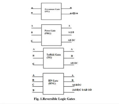
I. Feynman Gate:
It is a 2x2 gate and its logic circuit is as shown in the figure. It is also known as Controlled Not (CNOT) Gate. It has
quantum cost one and is generally used for Fan Out purposes.
2. Peres Gate:
It is a 3x3 gate and its logic circuit is as shown in the figure. It has quantum cost four. It is used to realize various
Boolean functions such as XOR, AND.
3. Toffoli Gate:
It is a 3x3 gate and its logic circuit is as shown in the figure. It has quantum cost two. It is used to realize various
Boolean functions such as XOR, AND.
4. HNG Gate:
It is a 4x4 gate and its logic circuit is as shown in the figure. It has quantum cost six. It is used for designing adders
like ripple carry adder. It reduces the garbage and gate counts by producing the sum and carry in the same gate.
55 |
P a g e
IV.URDHVA TIRYAKBHAYAM MULTIPLICATION ALGORITHM
Among all the techniques used in Vedic Mathematics for multiplication, Urdhav Tiryagbhyam(UT) is the most
preferred technique. Urdhav Tiryagbhyam means vertically and crosswise multiplication. Urdhav Tiryagbhyam(UT)
was discovered to increase the speed of multiplication of decimal numbers, and it can also be used for binary
numbers multiplication. The partial products are generated in parallel, which provides fast multiplication. The
biggest advantage of UT is that, it can be implemented with reduced number of AND gates, Full and Half Adders.
Consider an example, which multiply two decimal numbers 234*152, as shown in Fig. 2. Firstly we take the product
of least significant bits (LSB) of the multiplier and multiplicand, the least significant bit of the result i.e. 8 in this
case, is stored and there is no carry is generated for the next step. In the next step, crosswise two least significant bits
are multiplied, and their product is added with the previous carry. Similarly in the next step all the bits are multiplied
crosswise and their products are summed up with the previous carry. Again In the next step, two most significant
bits are multiplied crosswise, and results are added in the similar manner.
And finally, the most significant bit(MSB) of the multiplier and multiplicand are multiplied, and result is added
with the previously generated carry, to get the end result. The binary number multiplication can be done in the same
manner. As shown in Fig. 3, the bits of multiplier and multiplicand are multiplied crosswise. These results are added
with previous carry, to generate the result of that particular step. The final result is obtained by concatenating, the
result from each step and the carry in the last step.
56 |
P a g e
Fig.3.Urdhva tiryakbhayam algorithm for binary multiplication
V.ARCHITECTURE OF REVERSIBLE URDHVA TIRYAKBHAYAM MULTIPLIER
The digital logic implementation of the 4x4 UT Multiplier using the conventional logic gates is shown in figure 4.
The expressions for the eight output bits are given below. The reversible implementation is shown in figure 5. This
circuit requires a total of 30 reversible logic gates out of which 16 are Toffoli Gate, 7 are HNG gates, and 6 are
Peres gate, one Feynman gate. The quantum cost of the 4x4 UT Multiplier is 90, the total number of gates used will
be 30, the number of garbage output will be 52 and the number of constant inputs will be 29.
57 |
P a g e
P0 = a0b0c1p1 = a1b0 + a0b1
c3c2p2 = a2b0 + a1b1 + a0b2 + c1
c5c4p3 = a3b0 + a2b1 + a1b2 + a0b3 + c3c2
c7c6p4 = a3b1 + a2b2 + a1b3 + c5c4
c9c8p5 = a3b2 + a2b3 + c7c6
p7p6 = a3b3 + c9c8
Fig. 5. RTL Schematic of Reversible 4x4 UT multiplier
VI.RESULTS, ANALYSIS AND COMPARISONS
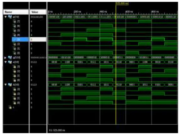
The design of the reversible 4x4 Vedic Multiplier is logically verified using XILINX 14.7. The simulation result is
shown in figure 6.
58 |
P a g e
The TRILC can be considered as a parameter which reflects the overall performance of the reversible logic circuit.TRLIC=∑(NG,CI,QC,GO)
Where NG is the number of gates in the reversible logic. CI is the number of constant inputs. QC is the quantum
cost of the circuit. GO is the number of garbage outputs.
The important design constraints of the reversible logic circuits are
1. Reversible logic circuit should have minimum quantum cost.
2. The design can be optimized so as to produce minimum number of garbage outputs.
3. The reversible logic circuits must use minimum number of constant inputs.
4. The reversible logic circuits must use minimum number of reversible gates.
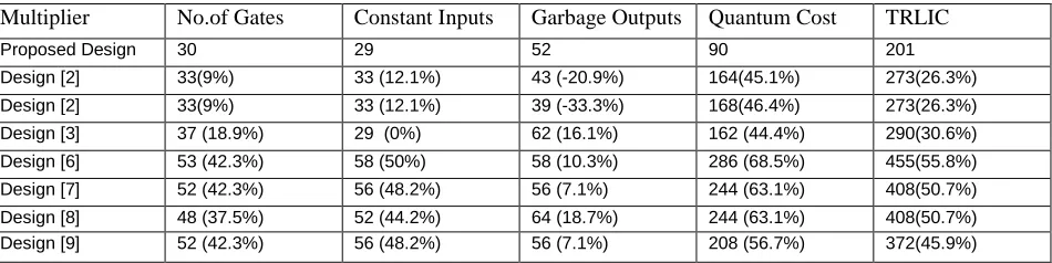
Our proposed design is compared with different reversible multiplier given in the reference in terms of number of
gates, constant inputs, garbage outputs, quantum cost and also in terms of TRLIC values which is shown in table1.
Compared to the best design in the table with 33 gates [2] our design has 30 gates results in 9% decrease. Quantum
cost of the proposed design is 90 compared to best design [3] which has a quantum cost 162 result in decrease in
44.4%. The TRLIC of proposed design is 201 compared to the best design [2] which has 273 which gives the
improvement of 26.3%. So we can say that proposed design is better than all the compared designs.
Table 1. Comparison of multiplier designs
Multiplier No.of Gates Constant Inputs Garbage Outputs Quantum Cost TRLIC
Proposed Design 30 29 52 90 201
Design [2] 33(9%) 33 (12.1%) 43 (-20.9%) 164(45.1%) 273(26.3%)
Design [2] 33(9%) 33 (12.1%) 39 (-33.3%) 168(46.4%) 273(26.3%)
Design [3] 37 (18.9%) 29 (0%) 62 (16.1%) 162 (44.4%) 290(30.6%)
Design [6] 53 (42.3%) 58 (50%) 58 (10.3%) 286 (68.5%) 455(55.8%)
Design [7] 52 (42.3%) 56 (48.2%) 56 (7.1%) 244 (63.1%) 408(50.7%)
Design [8] 48 (37.5%) 52 (44.2%) 64 (18.7%) 244 (63.1%) 408(50.7%)
Design [9] 52 (42.3%) 56 (48.2%) 56 (7.1%) 208 (56.7%) 372(45.9%)
VII.CONCLUSIONS
This paper presents the 4x4 Urdhva Tiryakbhayam Vedic Multiplier realized using reversible logic gates. First the
4x4 Vedic Multiplier is designed using full adders, half adders, and gates and xor gate. The full adders are replaced
with HNG gates, half adders are replaced with PRG gates, and gates are replaced with Toffoli Gates and XOR gate
is replaced with Feynman Gate.
The proposed design has minimum number of gates , minimum number of constant inputs, minimum number of
59 |
P a g e
the table. If we see the performance parameter called TRLIC which is defined as sum of all cost metrics of the givendesign. This design performs better than all the other studied reversible multipliers and requires less area. The
quantum cost is a parameter that directly reflects the delay of the quantum circuit. Also lower TRLIC means lower
the quantum cost, hence lower is the delay and vice versa.
REFERENCES
[1] Swami Bharati Krsna Tirtha, Vedic Mathematics. Delhi:Motilal Banarsidass publishers 1965
[2] Rakshith T R and Rakshith Saligram,” Optimized Reversible Vedic Multipliers for High Speed Low Power
Operations” Proceedings of 2013 IEEE Conference on Information and Communication Technologies (ICT
2013)
[3] Rakshith T R and Rakshith Saligram, Design of High SpeedLow Power Multiplier using Reversible logic: a
Vedic Mathematical Approach, Intl. Conf. on Circuit, Power and Computational Technologies
[4] Landauer,"Irreversibility and Heat Generation in the computational Process", IBM Journal of Research and
Development, 5, pp.183-191, 1961.
[5] C.H. Bennett, "Logical reversibility of Computation", IBM J. Research and Development, pp.525-532,
November 1973.
[6] H. Thapliyal and M.B. Srinivas, "Novel Reversible multiplier Architecture Using Reversible TSG Gate",
Proc. IEEE International Conference on Computer Systems and Applications, pp. 100-103, March 2006.
[7] Shams, M., M. Haghparast and K. Navi, Novel reversible multiplier circuit in Nanotechnology. World Appl.
Sci. J.,,3(5): 806-810.
[8] Somayeh Babazadeh and Majid Haghparast, "Design of a Nanometric Fault Tolerant Reversible Multiplier
Circuit" Journal of Basic and Applied Scientific Research, 2012.
[9] M. Haghparast et al. , "Design of a Novel Reversible multiplier Circuit using HNG Gate in Nanotechnology,"
in World Applied Science Journal, Vol. 3, No. 6, pp. 974-978, 2008.
[10] Thapliyal, H., M.B. Srinivas and H.R. Arabnia, 2005, A Reversible Version of 4x4 Bit Array Multiplier with
Minimum Gates and Garbage Outputs, Int. Conf. embedded System, Applications (ESA'05), Las Vegas,
USA, pp: 106-114.
[11] H. Thapliyal and M.B. Srinivas, "Reversible Multiplier Architecture Using TSG Gate", Proc. IEEE
InternationalConference on Computer Systems and Applications, pp. 241- 244, March 2007.
[12] M. S. Islam et al. , "Realization of Reversible Multiplier Circuit," in Information Tech. 1, Vol. 8, No. 2, pp.
117-121, 2005.
[13] K. Navi, M. Haghparast, S. JafaraliJassbi, O. Hashemipour, Design of a novel reversible multiplier circuit
60 |
P a g e
[14] M. Shams et al., "Novel Reversible Multiplier Circuits in Nanotechnology," in World Applied ScienceJournal, Vol. 3, No. 5, pp, pp. 806- 810, 2008.
[15] M S Islam, M M Rahman, Z Begum and M Z Hafiz, 2009. Low Cost Quantum Realization of Reversible