for IEEE 802.11N WLAN Applications
Minoh Son, Jinho Yoo, Changhyun Lee, and Changkun Park*
Abstract—In this work, we propose a balun embedded driver stage to enhance the bandwidth and minimize the chip size of a differential CMOS power amplifier. By removing the passive input transformer, the bandwidth and chip size are improved. The proposed driver stage acts as an input balun as well as the driver stage for the power stage. The proposed driver is composed of a cascade connected PMOS, an inductor, and NMOS to generate the differential output signal. For the function of the input balun, the gate of the PMOS is connected to the drain of the NMOS. To verify the feasibility of the proposed balun embedded driver stage, we design a differential CMOS power amplifier for 5-GHz IEEE 802.11n WLAN applications. The designed power amplifier is fabricated using the 180-nm SOI RF CMOS process. The measured 3-dB bandwidth is approximately 2.5 GHz. The chip size of the fully integrated power amplifier, including input and output matching networks and test pads, is 0.885 mm2. The measured maximum output power is 20.18 dBm with a PAE of 10.16%.
1. INTRODUCTION
In general, most power amplifiers have been designed using III-V compound semiconductors because of the high linearity and breakdown voltage [1–6]. Additionally, given that the compound semiconductor process provides a through-hole via and thereby allows utilization of the back metal layer as a ground (GND) plane, a high quality GND level can be obtained using compound semiconductor based power amplifiers. By virtue of the high quality GND level in compound semiconductors, most III-V power amplifiers have been designed with a single-ended structure.
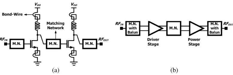
However, recently, CMOS power amplifiers are under vigorously study in hopes of reducing the overall unit cost of production of RF systems [7–14]. One of the many advantages of the CMOS power amplifier is that it can be integrated with digital control blocks and analog circuits to complete a fully integrated SoC [15, 16]. Although the linearity and breakdown voltage of CMOS amplifiers are lower than those of HBT amplifiers, various techniques to overcome the weaknesses of the CMOS process have been studied. For example, a distributed active transformer (DAT) can be introduced to overcome the low breakdown voltage of CMOS and thereby successfully generate watt-level output power using CMOS power amplifiers [17, 18]. Accordingly, the good functionality of CMOS power amplifiers has been successfully proved through various meaningful studies. However, the structure of a CMOS power amplifier must be modified compared to that of an HBT power amplifier. Given that there is no through-hole via in the CMOS process, CMOS power amplifiers are often designed using a differential structure, while HBT power amplifiers are designed using a single-ended structure. If the CMOS power amplifier is designed using a single-ended structure, as shown in Fig. 1(a), gain reduction problems induced by the bond-wire are unavoidable. Additionally, the variations of the lengths and shapes of the bond-wires can lead to performance variation of the CMOS power amplifier. Given that a virtual AC
Received 7 December 2018, Accepted 16 January 2019, Scheduled 1 March 2019
* Corresponding author: Changkun Park ([email protected]).
WLAN application requires approximately 1 GHz of bandwidth in the power amplifier.
(b) (a)
Figure 1. Simple block-diagrams of typical RF CMOS power amplifiers (a) with single-ended and (b) differential structures.
In this work, we propose an active input balun to reduce the overall chip area and to solve the narrow bandwidth problems of differential CMOS power amplifiers. In Section 2, we show the problems of the typical differential structure, which are related to the layout area and bandwidth. The structure of the proposed active input balun will be presented in Section 3. In Sections 4 and 5, to verify the functionality of the proposed active input balun, the design of the power amplifier using the proposed active input balun and the measured results, respectively, are presented.
2. TYPICAL DIFFERENTIAL CMOS POWER AMPLIFIER
Compared to a single-ended structure, a differential structure requires input and output baluns. In general, an output balun is composed of a transformer and MIM capacitors, as shown in Fig. 2(a). As shown in Fig. 2(a), the transformer acts as the output balun at the same time as it is used for the output matching network. Additionally, the turn ratio of the primary and secondary windings of the transformer takes on the important role of impedance transformation, allowing the power amplifier to obtain watt-level output power. Consequently, given that the output transformer, which is essential in the differential structure, also acts as the output matching network, the chip area and bandwidth of the output matching network for the differential structure are nearly identical to those of the single-ended structure.
Figure 2(b) shows the inter-stage matching network in the differential power amplifier. In general, a shunt inductor is used between differential signal lines to cancel out the parasitic gate capacitances of the power stage. However, the requirements of the shunt inductor in the input part of the power stage are common issues in the differential and single-ended structures. Accordingly, the chip area and bandwidth issues of the inter-stage matching network for the differential structure are nearly identical to those for the single-ended structure.
(b) (a)
Figure 2. Simple schematics of (a) output and (b) inter-stage matching networks for the differential power amplifiers.
Figure 3. Simple schematic of the input part of the differential power amplifier.
of the power stage; the required inductance of the secondary winding of the input transformer is higher than that of the inductor in the inter-stage matching network. Accordingly, to obtain high inductance of the secondary winding of the input transformer, the input transformer should be designed as a spiral, thereby increasing the overall chip area. On the other hand, given that the parasitic gate capacitance of the driver stage is negligible compared to that of the power stage, the input shunt inductor, which is implemented using the secondary winding of the input transformer in the differential structure, can be omitted in the single-ended structure.
Consequently, compared to the singled-ended power amplifier, the differential power amplifier has certain drawbacks because of the requirements of the input transformer. To provide an intuitive view of the chip area, Fig. 4 shows the layout of the key circuit blocks of the differential power amplifier. As can be seen in Fig. 4, the input transformer for the differential power amplifier requires considerable chip area, which is not essential in the single-ended power amplifier. Moreover, both sides of the input transformer are wasted if additional digital and analog blocks are not located on both sides of the input transformer.
(b) (a)
Figure 5. Gains of (a) each building block and (b) entire power amplifier with differential structure.
Figure 5(a) shows the gains of each of the building blocks of the differential power amplifier. Given that the input transformer is designed as a spiral, the resistive loss of the input matching network with the input transformer is higher than that of the output matching network with an output transformer, as can be seen in Fig. 5(a). In Fig. 5(a), where we show that the gain of the driver stage is higher than that of the power stage because, to generate watt-level output power in general, power matching is adapted in the power stage. Although the frequency responses of each building block may be one of several types including loss-pass filter, high-pass filter, and band-pass filter, for the sake of simplicity of description, we assume that all of the building blocks present frequency responses of the band-pass filter type.
Nevertheless, if the bandwidths of each block are sufficiently wide, the entire bandwidth of the power amplifier, which is composed of the described building blocks, may present narrow bandwidth characteristics, as shown in Fig. 5(b). In general, the bandwidth requirements in most types of wireless communications are narrow. However, some recent developments in wireless communication require very wide bandwidth characteristics to provide communications with high data rate. For example, a 5-GHz IEEE 802.11n WLAN application requires approximately 1 GHz bandwidth from the power amplifier. Accordingly, for 5-GHz IEEE 802.11n WLAN power amplifiers, an additional technique to allow for wide bandwidth is essential. One solution can be to remove the input transformer, which contributes to restricting the overall bandwidth. Moreover, if the input transformer is removed, the gain of the power amplifier can be improved by the amount of the loss of the input transformer.
In this work, as shown in Fig. 6, we propose an active balun embedded driver stage in a differential CMOS power amplifier for 5-GHz IEEE 802.11n WLAN applications. One of the most significant issues in this work is that the driver stage should act as the input balun to allow the removal of the bulky input transformer, thereby reducing the overall chip area and widening the bandwidth of the differential CMOS power amplifier.
Figure 6. Block-diagram of the proposed active balun embedded driver stage for the differential CMOS power amplifier.
3. PROPOSED ACTIVE BALUN EMBEDDED DRIVER STAGE
(b)
(a) (c)
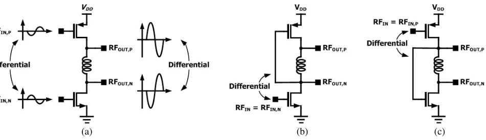
Figure 7. Simple schematics of the proposed balun embedded driver stage: (a) preliminary structure, (b) PMOS gate — NMOS drain coupled structure, and (c) NMOS gate — PMOS drain coupled structure.
Fig. 7. As can be seen in Fig. 7(a), if the driver stage consists of a PMOS, an Inductor, and NMOS with cascade connection; when RFIN,P and RFIN,N are in a differential relationship, the amplified signals, RFOUT,P and RFOUT,N, are also in a differential relationship, as shown in Fig. 7(a). However, in this case, an input balun to convert the single ended signal to the differential signal of RFIN,P and RFIN,Nis still required. To remove this requirement of an input balun, as can be seen in the schematic shown in Fig. 7(a), the gate node of the PMOS is connected to the drain node of the NMOS, as shown in Fig. 7(b). Given that the drain node of the NMOS is opposite to the gate node of the NMOS, the gate nodes of the NMOS and PMOS are in a differential relationship. With a single-ended signal, RFIN,N, which can be renamed RFIN, and the differential output signals, RFOUT,P and RFOUT,N, can then be presented. Another modification is shown in Fig. 7(c). In Fig. 7(c), the gate node of the NMOS is connected to the drain node of the PMOS. Similarly, a single-ended signal, RFIN,P, which can be renamed RFIN, and the differential output signals, RFOUT,P and RFOUT,N, can be presented.
As described above, the operating principles of the proposed active baluns shown in Figs. 7(b) and (c) are identical to each other. However, given that the mobility of the PMOS is lower than that of the NMOS, the total gate width of the PMOS should be larger than that of the NMOS to equalize the DC current of the PMOS with that of the NMOS. Accordingly, given that the input impedances for RFIN,P, shown in Fig. 7(c), should be lower than that for the RFIN,N, shown in Fig. 7(b), the gain of the schematic shown in Fig. 7(c) may lower than that shown in Fig. 7(b). Consequently, we choose the type of proposed active balun shown in Fig. 7(b). Compared to the simple schematic of the input part of the typical differential CMOS power amplifier shown in Fig. 3, in the active balun shown in Fig. 7, the number of required inductors is identical to that of the typical driver stage. However, given that the proposed active balun embedded driver stage shown in Figs. 7(b) and (c) acts as an input balun and also as a driver stage, the transformer can be removed in the proposed active balun embedded driver stage. Consequently, using the proposed balun embedded driver stage, issues related to chip area and operating bandwidth can be solved in the differential CMOS power amplifier.
4. DESIGN OF THE PROPOSED DIFFERENTIAL CMOS POWER AMPLIFIER
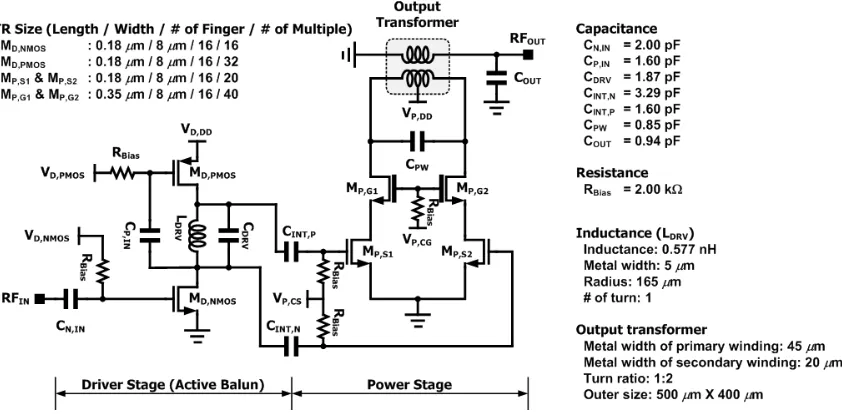
Figure 8. Schematic of the proposed differential CMOS power amplifier using a balun embedded driver stage.
seen in Fig. 8, given that no virtual ground is generated in the proposed balun embedded driver stage, the bond-wires essential in the VD,DD node and GND node for the driver stage may degrade the overall performance of the power amplifier. Fortunately, the effect of the parasitic inductance of the bond-wires on the performance of the power amplifier is negligible because the current flowing through the driver stage is much smaller than that flowing through the power stage and, hence, the source impedances of MD,PMOS and MD,NMOS are sufficiently large to allow us to ignore the parasitic inductance of the bond-wires.
Although the cascode structure is regarded as a popular solution to mitigate the reliability problems in CMOS amplifiers, this structure is not used in the balun embedded driver stage. As can be seen in Fig. 8, the supply voltage, VD,DD, for the driver stage is divided into MD,PMOS and MD,NMOS. Accordingly, in spite of the lack of a cascode structure, the voltage stress is mitigated in the proposed driver stage, unlike the case of a typical common-source amplifier structure. In this study, to prevent breakdown of MD,NMOSand MD,PMOS, we control the peak drain-source voltage to be lower than 3.0 V. The peak drain-source voltages of MD,NMOS and MD,PMOS are controlled by the values of CDRV and LDRV shown in Fig. 8 [21]. Additionally, the peak voltage at the gate of MD,PMOScould be modulated by the value of CP,IN. Accordingly, the value of CP,INis also used to control the peak drain-source voltage of MD,PMOS to be lower than 3.0 V. Fig. 9 shows the time-domain drain-source voltages of MD,NMOS and MD,PMOS with the input power, PIN range of−40 dBm to 10 dBm.
The output signal in the drain node of the MD,PMOSis connected to the gate node of MP,S1 through the DC blocking capacitor. Similarly, the output signal in the drain node of the MD,NMOS is connected to the gate node of MP,S2through the DC blocking capacitor. Given that the output signals in the drain nodes of MD,PMOS and MD,NMOS are differential, the power stage also shows differential operation.
To estimate the functionality of the proposed active balun, we simulate the phase and magnitude differences between the differential signals in the input nodes of the power stage. To improve the simulation accuracy, all of the interconnection lines are taken into account using a 2.5-dimensional electromagnetic (2.5-D EM) simulation. Fig. 10 shows the gain of the designed power amplifier and phase difference between the differential signals in the gate nodes of MP,S1 and MP,S2. The simulated input P1dB of the designed power amplifier is approximately 0 dBm with power gain of 19.4 dB. As shown in Fig. 10, the phase difference between the differential signals is gradually distorted with input power higher than 0 dBm. Fig. 11 shows the voltage difference and the magnitude of voltages in the gate nodes of MP,S1 and MP,S2. As can be seen in Fig. 11, the voltage difference between the differential signals is lower than 35 mV with input power lower than 0 dBm.
Figure 9. Simulated drain-source volt-ages, VDSs of MD,NMOS and MD,PMOS (Fre-quency = 5.3 GHz).
Figure 10. Simulated phase difference of the differential signal in the input nodes of the power stage and power gain of the power amplifier (Frequency = 5.3 GHz).
Figure 11. Simulated voltage difference of the differential signal in the input nodes of the power stage (Frequency = 5.3 GHz).
Figure 12. Simulated gain of the power amplifier.
supply voltage VP,DD for the power stage enters through the center tap of the primary winding of the output transformer because the virtual ground is generated at the center of the primary winding for the fundamental frequency. The output transformer is used as the output balun as well as being used as one of the output matching components. The output transformer is designed using a 2.5-D EM simulator. Fig. 12 shows the simulated gain of the designed power amplifier.
5. EXPERIMENTAL RESULTS
Figure 13. Chip photograph of the designed power amplifier with proposed balun embedded driver stage.
proposed balun embedded driver stage, the input transformer, which is essential in typical differential CMOS power amplifiers, can be removed and only one inductor and one transformer are used. The chip size is 1.18×0.75 mm2. The outer size of the designed output transformer is 0.5×0.4 mm2, while the widths of the primary and secondary windings are 45µm and 20µm, respectively.
The supply voltage for the proposed balun embedded driver stage and power stage is 3.3 V for mobile applications. The input and output load impedances are set at 50 Ω. To verify the feasibility of the designed power amplifier, we use a continuous wave (CW) input signal and an IEEE 802.11n WLAN modulated signal with 64-QAM and 20 MHz bandwidth.
Figures 14 and 15 show the measured results for the CW input signal. As can be seen in Fig. 14, the measured 3-dB bandwidth is approximately 2.5 GHz, ranging from 3.3 GHz to 5.8 GHz, while the design target of the operating frequency ranges from 4.9 GHz to 5.85 GHz. From the measured frequency response shown in Fig. 14, the wide bandwidth of the proposed power amplifier is demonstrated. However, the peak performance, which is related to both the maximum output power (PMAX) and the power added efficiency (PAE), is obtained at 4.7 GHz.
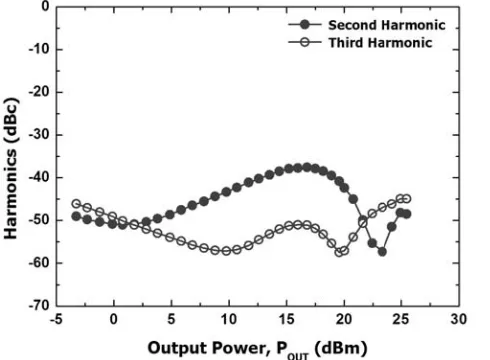
Figure 15. Measured results: second and third harmonics according to the output power with CW input signal.
Figure 16. Measured results: stability factors.
To verify the differential characteristics of the proposed balun embedded driver stage, we measure the second and third harmonic components, with results shown in Fig. 15. As can be seen in the measured results, the harmonic components are reasonably low compared to the fundamental component.
Additionally, given that the proposed balun embedded driver stage may generate an undesired oscillation feedback loop, we verify the stability characteristic, with results shown in Fig. 16. Judging from the measured stability factors, the designed power amplifier is unconditionally stable.
Figure 17 shows the frequency response for the IEEE 802.11n WLAN modulated input signal with 64-QAM, 20 MHz bandwidth, and 9.6 dB PAPR. As can be seen in Figs. 14 and 15, the gain with the modulated input signal, according to the operating frequency, is nearly identical to that with the CW input signal.
Figure 18 shows the measured EVM. To meet the standard of IEEE 802.11n WLAN with 64-AQM
Figure 17. Measured results: gain according to operating frequency with 802.11n WLAN modulated input signal.
Figure 19. Measured results: signal constella-tion with 802.11n WLAN modulated input signal.
Figure 20. Measured results: gain and PAE according to output power with 802.11n WLAN modulated input signal.
and 20 MHz bandwidth, the measured EVM should be lower than −28 dB. The measured maximum output power, PMAX, satisfies the standard, with a value of 20.18 dBm. In Fig. 19, the measured signal constellation at the maximum output power of 20.18 dBm is shown.
Figure 20 shows the measured gain and PAE with the WLAN-modulated input signal. The measured maximum average output power at which the WLAN specification is satisfied is 20.18 dBm, with a PAE of 10.16% and a gain of 15.8 dB. Fig. 21 shows the measured frequency spectrum at the maximum average output power with the 802.11n WLAN modulated input signal.
Table 1 provides results of recently reported CMOS power amplifiers for 5-GHz WLAN applications for comparison. Most recent works related to power amplifiers for 5.0-GHz WLAN applications are designed using 40-nm and 65-nm CMOS technology to meet the linearity requirement of the WLAN standard. In this study, we verify the possibility of a CMOS power amplifier using 180-nm CMOS technology for 5.0 GHz 802.11n WLAN applications.
Table 1. Comparison with state-of-the-art power amplifiers for 5-GHz WLAN applications.
Ref. [22] [23] [24] This work
Tech. 40-nm CMOS 45-nm CMOS 180-nm SOI CMOS 180-nm SOI CMOS Chip area
(mm2) 1.07 - 1.065 0.885
Modulation Signal 802.11ac (64-QAM) 802.11a (64-QAM) 802.11n (64-QAM) 802.11n (64-QAM) Bandwidth
(MHz) 20/40/80 20 20 20
Frequency
(GHz) 5.00 5.00 4.47 4.70
POUT @−28 dB
EVM (dBm) 18.7/17.3/13.6 N.A. 20.34 20.18
PAE @−28 dB EVM (%)
161)(@ 20 MHz BW)
141)(@ 40 MHz BW) N.A.
9 (@ 20 MHz BW)
Figure 21. Measured results: spectrum with 802.11n WLAN modulated input signal.
6. CONCLUSION
In this study, to improve amplifier bandwidth and to minimize the chip size, we design a CMOS power amplifier with an active balun. The proposed balun embedded driver stage acts as a driver stage for the power amplifier as well as acting as the input balun. By virtue of removing the bulky input transformer, the chip size of the designed power amplifier can be reduced compared to that of typical differential CMOS power amplifier. The bandwidth of the power amplifier with the proposed balun embedded driver stage is also improved. Given that the proposed driver stage is composed of a cascade connected PMOS, an inductor, and NMOS, the supply voltage of the driver stage is properly divided to mitigate reliability problems. Accordingly, the cascode structure is not utilized in the driver stage, unlike the case of a typical common-source amplifier. Additionally, given that the loss induced by the presence of a typical input transformer is removed, the gain of the power amplifier is improved. To verify the feasibility of the proposed balun embedded driver stage, we design a differential CMOS power amplifier using the 180-nm SOI RF CMOS process. An IEEE 802.11n WLAN modulated signal with 64-QAM, 20 MHz bandwidth, and 9.6 dB PAPR is used in the measurement. The measured maximum average output power is 20.18 dBm with a PAE of 10.16% and a chip size of 0.885 mm2. From the measured results for the power amplifier, the feasibility of the power amplifier is successfully verified.
ACKNOWLEDGMENT
This work was supported by the Technology Innovation Program (10053023) funded By the Ministry of Trade, industry & Energy (MI, Korea).
REFERENCES
1. Moon, K., Y. Cho, J. Kim, S. Jin, S. Kim, and B. Kim, “An HBT saturated power amplifier with minimized knee effect for envelope tracking operation,” IEEE Microw. Wireless Compon. Lett., Vol. 25, 544–546, 2015.
2. Lin, L., L. Zhou, R. Wang, L. Tong, and W.-Y. Lin, “Electrothermal effects on performance of GaAs HBT power amplifier during power versus time (PVT) variation at GSM/DCS bands,”IEEE Trans. Microw. Theory Techn., Vol. 63, 1951–1963, 2015.
3. Griffith, Z., M. Urteaga, P. Rowell, and R. Pierson, “A 6–10 mW power amplifier at 290–307.5 GHz in 250 nm InP HBT,” IEEE Microw. Wireless Compon. Lett., Vol. 25, 597–599, 2015.
4. Yoon, S., I. Lee, M. Urteaga, M. Kim, and S. Jeon, “A fully-integrated 40–222 GHz InP HBT distributed amplifier,” IEEE Microw. Wireless Compon. Lett., Vol. 24, 460–462, 2014.
2015.
10. Kaymaksut, E., D. Zhao, and P. Reynaert, “Transformer-based doherty power amplifiers for mm-wave applications in 40-nm CMOS,” IEEE Trans. Microw. Theory Techn., Vol. 63, 1186–1192, 2015.
11. Ryu, N., B. Park, and Y. Jeong, “A fully integrated high efficiency RF power amplifier for WLAN application in 40 nm standard CMOS process,” IEEE Microw. Wireless Compon. Lett., Vol. 25, 382–384, 2015.
12. Godoy, P. A., S. W. Chung, T. W. Barton, D. J. Perreault, and J. L. Dawson, “A 2.4-GHz, 27-dBm asymmetric multilevel outphasing power amplifier in 65-nm CMOS,”IEEE J. Solid-State Circuits, Vol. 47, 2372–2384, 2012.
13. Yoon, Y., J. Kim, H. Kim, K. H. An, O. Lee, Ch.-H. Lee, and J. S. Kenney, “A dual-mode CMOS RF power amplifier with integrated tunable matching network,” IEEE Trans. Microw. Theory Techn., Vol. 60, 77–88, 2012.
14. Ham, J., J. Bae, M. Seo, H. Lee, K. C. Hwang, K.-Y. Lee, and Y. Yang, “Dual-mode supply modulator for CMOS envelope tracking power amplifier integrated circuit,”Microw. Opt. Technol. Lett., Vol. 57, 1338–1343, 2015.
15. Kim, H., J. Bae, J. Ham, J. Gu, M. Seo, K. C. Hwang, K.-Y. Lee, C.-S. Park, and Y. Yang, “Efficiency enhanced CMOS digitally controlled dynamic bias switching power amplifier for LTE,” Microw. Opt. Technol. Lett., Vol. 57, 2315–2321, 2015.
16. Nakatani, T., D. F. Kimball, L. E. Larson, and P. M. Asbeck, “0.7–1.8 GHz multiband digital polar transmitter using watt-class current-mode class-D CMOS power amplifier and digital envelope modulation technique for reduced spurious emissions,” Int. J. Microw. Wirel. Technol., Vol. 5, 271–284, 2013.
17. Aoki, I., S. D. Kee, D. B. Rutledge, and A. Hajimiri, “Fully integrated CMOS power amplifier design using the distributed active-transformer architecture,”IEEE J. Solid-State Circuits, Vol. 37, 371–383, 2002.
18. Yang, H.-S., J.-H. Chen, and Y.-J. E. Chen, “A 1.2-V 90-nm fully integrated compact CMOS linear power amplifier using the coupled L-shape concentric vortical transformer,”IEEE Trans. Microw. Theory Techn., Vol. 62, 2689–2699, 2014.
19. Son, M., J. Yoo, and C. Park, “A linear CMOS power amplifier using class-D to reduce the number of required inductors,”Microw. Opt. Technol. Lett., Vol. 58, 565–569, 2016.
20. Jeong, H., G. Ko, H. Shin, I. Kang, and C. Park, “A CMOS power amplifier using split input and output transformers to minimize its chip area,” Microw. Opt. Technol. Lett., Vol. 58, 1443–1446, 2016.
21. Lee, C. and C. Park, “Design methodology for a switching-mode RF CMOS power amplifier with an output transformer,”Int. J. Microw. Wirel. Technol., Vol. 8, 471–477, 2016.
22. Francois, B. and P. Reynaert, “A fully integrated transformer-coupled power detector with 5 GHz RF PA for WLAN 802.11ac in 40 nm CMOS,” IEEE J. Solid-State Circuits, Vol. 50, 1237–1250, 2015.