2546 |
P a g e
Hybrid Variable Latency Carry Skip Adder With Parallel
Prefix Network
Ruma Khatoon
1, J. Mahesh
21
Pursuing M.Tech (DSCE) from Sri Visvesvaraya Institute of Technology & Science, Chowderpally,
Devarkadra, Mahabubnagar
2
Working as Assistant professor (ECE) from Sri Visvesvaraya Institute of Technology & Science,
Chowderpally, Devarkadra, Mahabubnagar
ABSTRACT
In this paper, we propose a carry skip adder (CSKA) architecture that has a good performance compared with the existing conventional method. The speed development is completed by applying some methods those are in-crementation concatenation methods to improve the efficiency of the conventional CSKA (Conv-CSKA) archi-tecture. Instead of using multiplexer logic in conventional architecture, the proposed architecture use AND-OR-Invert (AOI) and OR-AND-AND-OR-Invert (OAI) logic gates to skip the logic. The architecture may be recognized with permananet size of state and different stage size styles, wherein the later further develops the speed variables of the adder. Lastly, a the extension of the proposed architecture hybrid variable latency is, which is decreasing the power consumption without depending on the speed. This extension develops a modified parallel architec-ture for boosting the slack time, and hence, allowing further voltage reduction. The proposed architecarchitec-tures are evaluated by comparing their performance and efficiency with other adders. The proposed CSKA explains the decrementation of consumption power compared with the previous works in this process while improving the speed using XILINX ISE 14.5 simulation tool.
Keywords- Carry skip adder (CSKA), hybrid variable latency adders, voltage scaling.
I.
INTRODUCTION
Adders are fundamental obstruct in arithmetic and logic units (ALUs) and hence enhancing their speed and
de-creasing their energy utilization greatly involve the speed of processors. There are many efforts on the subject of
developing the speed of these units, which have been noted. Apparently, it is extremely fascinating to
at-tain higher speeds at low- po er/energy consumptions, that could be a challenge for the d signers of general
pur-pose processors.One of the effective techniques to decrease the facility consumption of digital circuits is to
de-crease the provision voltage owing to quadratic dependence of the change energy on the voltage. moreover, the
subthreshold current, that is that themain leak module in OFF devices, has associate degree exponential
de-pendence on the provision voltage level through the drain-induced barrier reducing result. supported the
num-ber of the provision voltage crease theoperationofONdevi es might reside withinthe superthreshold,
near-threshold, or subthreshold r gions. operating within thesuperthreshold region offers United States of
Amer-ica with lower delay and be ter change and leak powers compared with the near/subthreshold regions. within
2547 |
P a g e
threshold voltages. Moreover, these voltages ar (potentially) subject to method and environmental
varia-tions within the nanoscale technologies. The variavaria-tions increase uncertainties within the same performance
pa-rameters. in addition, the tiny subthreshold current causes an outsized delay for the circuits operational within
the subthreshold region.Recently, the near-threshold region has been consid-ered as a part that offers a a lot
of fascinating exchangepurpose be-tween delay and power dissipation compared thereupon of the subthreshold
one, as a result of it ends up in lower delay compared withthesubthresholdregion compared with the
super-threshold region. in addition, near-super-threshold operation, which utilizes supply voltage levels near the super-threshold
voltage of transistors, suffers considerably less from the process and environmental varia-tions compared with
the subthreshold region.
The dependence of the power (and presentation) on the supply voltage has been the motivation for design of
cir-cuits with the characteristic of dynamic voltage and frequency scaling. In these circir-cuits, to decrease the energy
consumption, the system may change the voltage (and frequency) of the circuit based on the workload
require-ment. For these systems, the circuit should be able to manage under a wide range of supply voltage levels. Of
course, achieving higher speeds at lower supply voltages for the computational blocks, with the adder as one the
main components, could be crucial in the design of high-speed, yet energy efficient, processors.
In addition to the knob of the supply voltage, one may prefer between different adder architectures/families for
developing power and speed. There are many adder families with different delays, power consumptions, and
area usages. Examples comprise carry increment adder (CIA), ripple carry adder (RCA), carry skip adder
(CSKA), carry select adder (CSLA), and parallel prefix adders (PPAs). The descriptions of each of these adder
architectures along with their characteristics may be established. The RCA has the simplest architecture with the
smallest area and power consumption but with the worst critical path delay. In the CSLA, the speed, power
utili-zation, and area traditions are considerably larger than those of the RCA. The PPAs, which are also called carry
look-ahead adders, extend direct parallel prefix structures to generate the carry as fast as possible. There are
different types of the parallel prefix algorithms that lead to different PPA structures with different performances.
As an example, the Kogge–Stone adder (KSA) is one of the fastest architectures but results in large power
con-sumption and area usage. It ought to be distinguished that the structure complexities of PPAs square measure a
lot of than those of alternative adder schemes.
The CSKA, that is associate economical adder in terms of power consumption and space usage, was projected.
The vital path delay of the CSKA is far smaller than the one within the RCA, whereas its space and power
con-sumption square measure the same as those of the RCA. in addition, the power-delay product (PDP) of the
CSKA is a smaller amount than those of the CSLA and PPA architec-tures. additionally, thanks to the
less variety of transistors, the CSKA advantages from comparatively short wiring lengths in addition as a
daily and straightforward layout.
The relatively lesser speed of this adder design, however, limits its use for high-speed applications.
The great characteristics of the CSKA design square measure given during this paper, we've focused
on reducing its delay by ever-changing its implementation supported the static CMOS log-ic.
the eye on the static CMOS derives from the necessity to own a systematically operational circuit underneath an
ou sized vary of provide voltages in greatly scaled technologies. The projected modification boosts the
addi-2548 |
P a g e
tion, associate adjustment of the design, supported the variable la-tency tecnique, that successively decreases the
ability consumption while not significantly effecting the CSKA speed, is additionally bestowed. There aren't
any tries directed on projected style of CSKAs performing from the superthreshold region right down to
near-threshold region and additionally, the projected style of (hybrid) inconsistent latency CSKA
struc-tures are explicit . Hence, the contributions of this paper may be reviewed as follows.
1) Introducing a made-to-order CSKA design by uniting the concatenation and therefore the incrementation
schemes to the conven-tional CSKA (Conv-CSKA) structure for developing the speed and energy potency of the
adder. The adjustment offers U.S.A. with the potential to use easier carry skip logics rely upon the AOI/OAI
compound gates rather than the electronic device.
2) Giving a design approach for building an efficient CSKA architecture based on logically expressions shown
for the criti-cal path delay.
3) Exploring the effect of voltage scaling on the efficiency of the proposed CSKA structure (from the nominal
supply voltage to the near-threshold voltage).
4) Establishing a hybrid variable latency CSKA architecture depend on the extension of the advised CSKA, by
replacing some of the middle stages in its structure with a PPA, which is changed in this paper.
The rest of this paper is organized as follows. Section II repesents the Conv-CSKA with fixed stage size (FSS)
and variable stage size (VSS) is discussed, while Section III shows the proposed static CSKA structure. Finally,
the conclusion is shown in Section V.
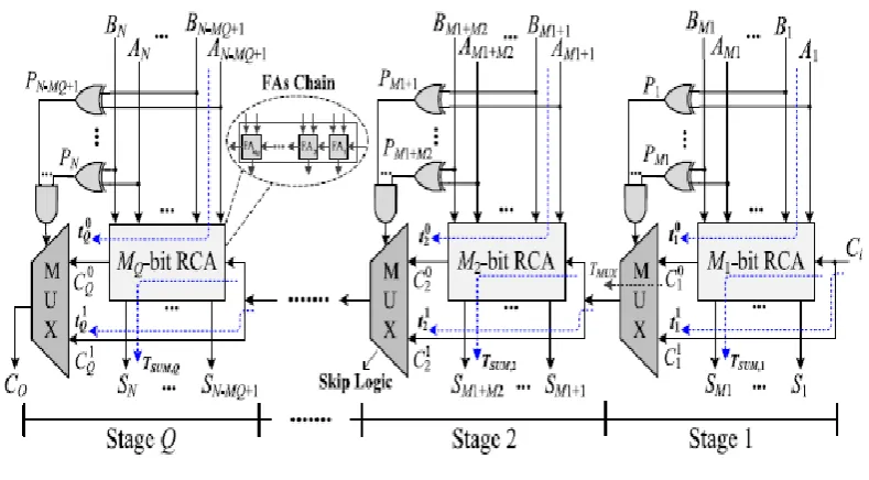
The design of associatedegree Nbit standard CSKA, that is rely on blocks of the RCA (RCA blocks), is shown
in Fig. 1. to boot the chain of FAs in every stage, there's a carry skip logic. For associate degree RCA that has N
cascaded FAs, A and B It indicates that the worst case delay belongs to the case wherever
where Pi is that the propagation signal associated with Ai and bismuth. This represents that the delay of the
RCA is linearly associated with N. within the case, wherever a bunch of cascaded FAs ar within the propagate
mode, the carry output of the chain is adequate to the carry input. within the CSKA, the carry skip logic
identi-fies this example, and makes the carry prepared for future stage while not expecting the operation of the
sylla-ble chain to be completed. The skip logic operate is performed victimization the gates and therefore
the electronic device as shown within the figure. rely on this justification, the N FAs of the CSKA ar collected
in letter stages. every stage includes associate degree RCA block with Mj FAs ( j = one, . . . , Q) and a skip logic.
In each stage, the inputs of the electronic device (skip logic) ar the carry input of the every stage and therefore
the carry output of its RCA block (FA chain). to boot, the merchandise of the propagation signals (P) of the
2549 |
P a g e
Fig. 1. standard structure of the CSKAThe CSKA is enforced victimization FSS andVSS wherever the very best speed is calculated for the VSS
struc-ture.
A. Fastened Stage Size CSKA
By forward that each stage of the CSKA contains M FAs, there ar letter = N/M stages wherever for the sake of
ease, we have a tendency to assume letter is associate degree whole number. The input signals of the j
th electronic device ar the carry output of the FAs chain within the j th stage described by C0j, the carry output
of the previous stage (carry input of the j th stage) described by C1j (Fig. 1).
The crucial path of the CSKA includes 3 parts: 1) the trail of the solfa syllable chain of the primary stage whose
delay is adequate to M × TCARRY; 2) the trail of the intermediate carry skip multi-plexer whose delay
is adequate to the (Q – 1)× TMUX; and 3) the trail of the solfa syllable sequence within the last stage whose its
delay is adequate to the (M −1) × TCARRY +TSUM. Note that TCARRY, TSUM, and TMUX are the propagation delays of
the carry output of an FA, the sum output of an FA, and the output delay of a 2:1 multiplexer, respectively.
Hence, the critical path delay of a FSS CSKA is made by
….(1)
Depend on (1), the optimal value of M (Mopt) that directs to optimum propagation delay may be estimated as
(0.5Nα)1/2 where α is equal to TMUX/TCARRY. Therefore, the optimum propagation delay (TD,opt) is achieved from
….(2)
B. Variable Stage Size CSKA
By giving variable sizes to the stages, the speed of the CSKA may be improved as mentioned. The speed
im-provement in this type is obtained by decreasing the delays of the first and third terms in (1). These delays are
2550 |
P a g e
one, whereas sizes of the following blocks may increase. To determine the rate of increase, let us express the
propagation delay of the C1j (t1j) by
….(3)
where t0j−1 (t1j−1) represents the estimating delay of C0j−1(C1j−1) signal in the ( j − 1)th stage. In a FSS CSKA,
except in thefirst stage, t0jis smaller than t
1
j. Hence, based on (3), the delayof t
0
j−1 may be increased from t01 to
t1j−1 without increasing thedelay of C1jsignal. This means that one could boost the sizeof the ( j − 1)th stage
(i.e., Mj−1) without increasing the propagation delay of the CSKA. Therefore, increasing the size of Mj for the j
th stage should be bounded by
….(4)
The last RCA block size also should be reduced when the increase in the stage size may not be continued to the
last RCA block. Thus, we validate the decrease in the RCA block sizes toward the last stage. First, note that
based on Fig. 1, the output of the j th stage is, in the worst case, accessible after t1j + TSUM, j. Assuming that the
pth stage has the maximum RCA block size, we wish to keep the delay of the outputs of the following stages to be equal to the delay of the output of the pth stage. We should reduce the size of the following RCA blocks ,to keep the same worst case delay for the critical path,. For example, when i ≥ p, for the (i +1)th stage, the output delay is t1i+ TMUX + TSUM,i+1, where TSUM,i+1 is the delay of the (i + 1)th RCA block for estimating all of its sum
outputs when its carry input is ready. Therefore, the size of the (i +1)th stage should be reduced to decrease
TSUM,i+1 stopping the increase in the worst case delay (TD) of the adder. In other words, we remove the boost in
the delay of the next stage due to the additional multiplexer by reducing the sum delay of the RCA block. This
may be logically expressed as
….(5)
This equation may be written in a more general form by replacing TMUX by TSKIP to allow for other
log-ic types instead of the multiplexer. For this form, α becomes equal to TSKIP/TCARRY. Finally, note that in real
im-plementations, TSKIP< TCARRY, and hence, [α/2] becomes equal to one. Then it can be written as
….(6)
III . PROPOSED HYBRID VARIABLE LATENCY CSKA
The basic theme behind victimizationVSS CSKA architectures was rely on nearly leveling the delays
of ways such the delay of the crucial path is reduced compared therewith of the FSS structure.This
re-moves U.S. from having the chance of victimization the slack time for the provision voltage scaling. to offer the
variable latency feature for the VSS CSKA structure, we have a tendency tore-place a number of the
cen-ter stages in our projected structure with a PPA modified during this paper. It ought tobe noted that since the
Conv-CSKA structure incorporates a less speed than that of the pro-posed CSKA, during thissection, we have a
tendency to don't take into account the conven-tional structure. The projected (hybrid variable latency) CSKA
structure is shown in Fig. a pair of wherever associate degree Mp-bit changed PPA is employed for the pth stage
(nucleus stage). Since the nucleus stage, that has the largest size (and delay) among the stages,
2551 |
P a g e
Thus, the employment of the quick PPA facilitates boosting the obtainable slack time within the variable latency
structure. It ought to be declareed that since the input bits of the PPA block area unit employed in the predictor
block, this block becomes components of each SLP1 and SLP2.
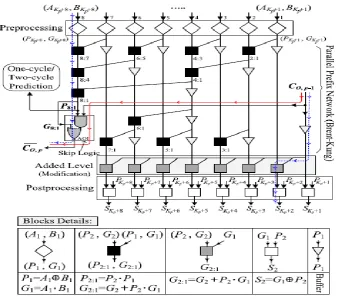
Fig. 2. Structure of the proposed hybrid variable latency CSKA
Fig. 3. Internal structure of the pth stage of the proposed hybrid variable latency CSKA
The prefix network of the Brent–Kung adder is employed for constructing the middle stage (Fig. 3) within
theprojected hybrid structure. one in every of the benefits of the this adder compared with alternative prefix
ad-ders is that during this structure, mistreatment forward ways, the longest carry is calculated sooner compared
with the intermediate carries, that ar computed by backward ways. to boot, the fan-out of adder is a smaller
amount than alternative parallel adders, whereas the length of its wiring is smaller. Finally, it's an easy and
regu-lar layout. the interior structure of the stage p, as well as the changed PPA and skip logic, is shown in Fig. 3.
Note that, for this figure, the scale of the PPA is assumed to be eight (i.e., Mp = 8).
In the preprocessing level, the propagate signals (Pi ) and generate signals (Gi ) for the
2552 |
P a g e
G8:1) of the prefix network along side P8:1, that is that the product of the all propagate signals of the
in-puts, ar calculable ahead of alternativeintermediate signals during this network as shown within the figure. The
signal P8:1 is employed within the skip logic to seek out out if the carry output of the previous stage (i.e.,
CO,p−1) ought to be skipped or not. additionally, this signal is developed because the predictor signal within
the variable latency adder. It ought to be mentioned that every one of those operations ar operated in parallel
with alternative stages.
Within the case, wherever P8:1 is one, CO,p−1 ought to skip this
stage conniving thatsome important ways ar started. instead, once P8:1 is zero, CO,p is adequate the G8:1. to
boot, no important path are activated during this case. once the parallel prefix network, the intermediate
car-ries, that ar functions of CO,p−1 and intermediate signals, ar computed (Fig. 7). Finally, within
thepostprocess-ing level, the out-put sums of this stage ar calculable. It ought to be noted that this implementation relieson the
similar schemes of the concatenation and incrementation ideas employed in the CI-CSKA explained. It ought
tobe noted that the top a part of the SPL1 path from CO,p−1 to final summation results of the PPA block and
also thebeginning a part of the SPL2 ways from inputs of this block to CO,p belong to the PPA block (Fig. 3). to
boot, the same as the projected CI-CSKA structure, initial|the primary} purpose of SPL1 is that the first
in-put little bit of the primary stage, and also the last purpose of SPL2 is that the last little bit of the add outin-put of
the incrementation block of the stage alphabetic character.
The steps for locating the sizes of the stages within the hy-brid variable latency CSKA structure ar the same
as thoseexplained. Since the PPA design is a lot of economical once its size is adequate associate number power
of 2, we will choose a bigger size for the middle stage consequently. This involves that the third step
ex-plained therein section is modified. the larger size (number of bits), compared thereupon of the
mid-dle stage within the original CI-CSKA structure, results in the decrease within the variety of
stages moreover smaller delays for SLP1 and SLP2. Thus, the slack time will increase a lot of.
IV. SYNTHESIS AND SIMULATION RESULTS
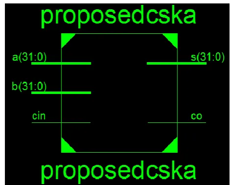
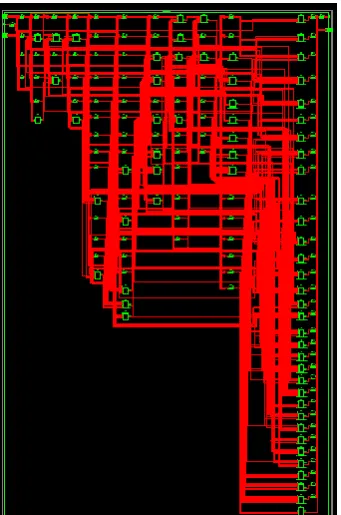
The proposed CI-CSKA is designed with the XILINX ISE 14.5 simulation tool and implemented with Verilog
HDL. The RTL diagram and simulation results are displayed below.
2553 |
P a g e
Fig. 5. Internal architectures of RTL diagram
Fig. 6. Synthesis report
2554 |
P a g e
V. CONCLUSION
In this paper, a static CMOS CSKA structure called CI-CSKA was proposed, which performs a higher speed
and lower energy consumption compared with those of the conventional one. The speed enhancement was
achieved by modifying the structure through the concatenation and incrementation techniques. In addition, AOI
and OAI compound gates were exploited for the carry skip logics. The effectiveness of the proposed architecture
for both FSS and VSS was revised by evaluating its power and delay with those of the Conventional CSKA,
RCA, CIA, SQRT-CSLA, and KSA structures. The proposed CSKA was designed by the Verilog HDL
synthe-sized in Xilinx ISE 14.5.
VI. FUTURE SCOPE
The present work has been designed for carry skip adder with better speed and low power consumption than the
conventional one. In future this work may be extended to improve in terms of area also.
REFERENCES
[1] I. Koren, Computer Arithmetic Algorithms, 2nd ed. Natick, MA, USA: A K Peters, Ltd., 2002.
[2] R. Zlatanovici, S. Kao, and B. Nikolic, “Energy–delay optimization of 64-bit carry-lookahead adders with a
240 ps 90 nm CMOS design example,” IEEE J. Solid-State Circuits, vol. 44, no. 2, pp. 569–583, Feb. 2009. [3] S. K. Mathew, M. A. Anders, B. Bloechel, T. Nguyen, R. K. Krishnamurthy, and S. Borkar, “A 4-GHz
300-mW 64-bit integer execution ALU with dual supply voltages in 90-nm CMOS,” IEEE J. Solid-State Cir-cuits, vol. 40, no. 1, pp. 44–51, Jan. 2005.
[4] V. G. Oklobdzija, B. R. Zeydel, H. Q. Dao, S. Mathew, and
R. Krishnamurthy, “Comparison of high-performance VLSI adders in the energy-delay space,” IEEE Trans.
Very Large Scale Integr. (VLSI)Syst., vol. 13, no. 6, pp. 754–758, Jun. 2005.
[5] B. Ramkumar and H. M. Kittur, “Low-power and area-efficient carry select adder,” IEEE Trans. Very Large
Scale Integr. (VLSI) Syst., vol. 20, no. 2, pp. 371–375, Feb. 2012.
[6] M. Vratonjic, B. R. Zeydel, and V. G. Oklobdzija, “Low- and ultra low-power arithmetic units: Design and comparison,” in Proc. IEEE Int. Conf. Comput. Design, VLSI Comput. Process. (ICCD), Oct. 2005, pp.
249–252.
[7] C. Nagendra, M. J. Irwin, and R. M. Owens, “Area-time-power tradeoffs in parallel adders,” IEEE Trans.
Circuits Syst. II, Analog Digit. SignalProcess., vol. 43, no. 10, pp. 689–702, Oct. 1996.
[8] Y. He and C.-H. Chang, “A power-delay efficient hybrid carrylookahead/ carry-select based redundant
bi-nary to two’s complement converter,” IEEE Trans. Circuits Syst. I, Reg. Papers, vol. 55, no. 1, pp. 336–
346, Feb. 2008.
[9] C.-H. Chang, J. Gu, and M. Zhang, “A review of 0.18 μm full adder performances for tree structured arith-metic circuits,” IEEE Trans. VeryLarge Scale Integr. (VLSI) Syst., vol. 13, no. 6, pp. 686–695, Jun. 2005.
[10] D. Markovic, C. C. Wang, L. P. Alarcon, T.-T. Liu, and J. M. Rabaey, “Ultralow-power design in
2555 |
P a g e
AUTHOR DETAILS
RUMA KHATOON, pursuing M.Tech (DSCE) from Sri Visvesvaraya Institute Of
Technology & Science, Chowderpally (Vill), Devarkadra (Mdl), Mahabubnagar
(Dist), TS, INDIA.
J. MAHESH, working as Assistant professor (ECE) from Sri Visvesvaraya
Insti-tute Of Technology & Science, Chowderpally (Vill), Devarkadra (Mdl), Mahabu