Firmware Package
User’s Manual
Part 1 and 2
PPCBUGA1/UM5 and PPCBUGA2/UM5
All rights reserved.
Printed in the United States of America.
Motorola® and the Motorola symbol are registered trademarks of Motorola, Inc. PowerPC™ is a trademark of IBM, and is used by Motorola with permission.
AIXTM is a trademark of IBM Corp.
While reasonable efforts have been made to assure the accuracy of this document, Motorola, Inc. assumes no liability resulting from any omissions in this document, or from the use of the information obtained therein. Motorola reserves the right to revise this document and to make changes from time to time in the content hereof without obligation of Motorola to notify any person of such revision or changes.
Electronic versions of this material may be read online, downloaded for personal use, or referenced in another document as a URL to the Motorola Computer Group website. The text itself may not be published commercially in print or electronic form, edited, translated, or otherwise altered without the permission of Motorola, Inc.
It is possible that this publication may contain reference to or information about Motorola products (machines and programs), programming, or services that are not available in your country. Such references or information must not be construed to mean that Motorola intends to announce such Motorola products, programming, or services in your country.
Limited and Restricted Rights Legend
If the documentation contained herein is supplied, directly or indirectly, to the U.S. Government, the following notice shall apply unless otherwise agreed to in writing by Motorola, Inc.
Use, duplication, or disclosure by the Government is subject to restrictions as set forth in subparagraph (b)(3) of the Rights in Technical Data clause at DFARS 252.227-7013 (Nov. 1995) and of the Rights in Noncommercial Computer Software and Documentation clause at DFARS 252.227-7014 (Jun. 1995).
About This Manual
Summary of Changes ... xvi
Overview of Contents ...xvi
Comments and Suggestions ...xviii
Conventions Used in This Manual...xviii
CHAPTER 1 General Information
Dump Memory to Tape ... B-2 Using the Service Call Function ... B-5 Operation ... B-5 Sending Messages ... B-7 Concurrent Mode ... B-7 Terminating the Conversation and Concurrent Modes ... B-8 Manual Connection ... B-9 Terminal Connection ... B-10
APPENDIX C PPCBug Messages
Introduction ... C-1 Error Messages ... C-2 Other Messages... C-3
APPENDIX D S-Record Format
Introduction ... D-1 S-Record Content ... D-1 S-Record Types... D-2 Creating S-Records... D-3 Example ... D-4
APPENDIX E Disk and Tape Controllers
Disk and Tape Support ...E-1 Floppy Drive Configuration Parameters...E-2
APPENDIX F Disk Status Codes
The PPCBug Firmware Package User’s Manual provides information on the PPCBug firmware, the start-up and boot routines, the debugger commands, the one-line assembler/disassembler, and the debugger system calls.
Information in this manual applies to Motorola PowerPC™-based boards that use PPCBug as its resident debugger program. The majority of Motorola’s PowerPC™-based boards including most VME, CompactPCI and ATX form factors are equipped with PPCBug.
This document is bound in two parts:
Part 1 (PPCBUGA1/UM5) contains the Table of Contents, List of Figures, and List of Tables for Chapters 1 through 3, Chapters 1 through 3 and the Index.
Part 2 (PPCBUGA2/UM5) contains the Table of Contents and List of Tables for Chapters 4 and 5 and Appendices A through H, and Chapters 4 and 5, Appendixes A through H, and the Index.
This is the fifth edition of the PPCbug Firmware Package User’s Manual. It supersedes the fourth edition (UM4) and incorporates the following updates.
Overview of Contents
Chapter 1, General Information, provides an overview of PPCBug,
memory requirements, an explanation of the start-up process, a "high-level" list of what PPCBug checks, a list of the LED/Serial startup diagnostic codes, a brief explanation on how to run the Debugger and Diagnostics firmware interactively, an explanation of the auto boot
Where Updated Description of Change
Overall Change Most instances of PPC1Bug or PPC1 were changed to PPCxBug or PPCx to accommodate multiple versions of Bug, which have been released.
Chapter 1 Since PPCBug resides on most PowerPC boards, specific boards are no longer listed at the beginning of this chapter. A correction was made to the starting address (from $03F80000 to $03F40000) of the example described in the section titled Memory Requirements on page 1-3.
A second example for the size and address requirements of NVRAM was added in the sections titled Size and Address Requirements for NVRAM on page 1-3.
New LED/Serial Startup Diagnostic codes were added to Table 1-1 on page 1-8.
The section titled Multiprocessor Support (Remote Start) on page 1-31 was completely revised.
Chapter 3 Several new commands were added (e.g., CACHE, IBM and MMGR), and several existing command descriptions were updated (e.g., ENV, NIOT, SROM, and TA).
Appendix G The content was completely revised from the previous version of this manual.
description of the types of board failures, an explanation of the MPU clock speed calculation, a description of the disk I/O support, a description of the network I/O support, and an explanation of the multiprocessor support (remote start).
Chapter 2, Using the Debugger, contains a series of explanations on the various aspects of Debugger use including such subjects as command syntax, command arguments, command options, control characters, entering and debugging programs, system call routines in user programs, preserving the operating environment, context switching, and floating point support.
Chapter 3, Debugger Commands, a list of all current commands, and a detailed explanation of each command including command input and description.
Chapter 4, One-Line Assembler/ Disassembler, describes a PPCBug tool
that allows you to create, modify and debug code written in PowerPC assembly language.
Chapter 5, System Calls, describes the PPCBug System Call handler, which allows system calls from user programs.
Appendix A, Related Documentation, lists related Motorola
documentation, as well as other vendor documents and specifications.
Appendix B, System Menu, describes each menu item within the PPCx-Bug> or PPCx-Diag> environment.
Appendix C, PPCBug Messages, contains a series of tables listing all PPCBug messages and their meaning.
Appendix D, S-Record Format, describes the purpose and use of the S-Record format.
Appendix E, Disk and Tape Controllers, lists and describes the types of disk and tape controllers supported by PPCBug.
standard PPCBug commands from a PowerPC board with a compatible network connectivity device.
Appendix H, Network Communication Status Codes, lists and describes two main types of network communication status codes: controller independent and controller dependent.
Comments and Suggestions
Motorola welcomes and appreciates your comments on its documentation. We want to know what you think about our manuals and how we can make them better. Mail comments to:
Motorola Computer Group Reader Comments DW164 2900 S. Diablo Way Tempe, Arizona 85282
You can also submit comments to the following e-mail address:
In all your correspondence, please list your name, position, and company. Be sure to include the title and part number of the manual and tell how you used it. Then tell us your feelings about its strengths and weaknesses and any recommendations for improvements.
Conventions Used in This Manual
The following typographical conventions are used in this document:
bold
is used for user input that you type just as it appears. Bold is also used for commands, options and arguments to commands, and names of programs, directories and files.
new terms.
courier
is used for system output (for example, screen displays, reports), examples, and system prompts.
<Enter>, <Return> or <CR>
<CR> represents the carriage return or Enter key.
CTRL
represents the Control key. Execute control characters by pressing the Ctrl key and the letter simultaneously, for example, Ctrl-d.
|
separates two or more items from which to choose (one only)
[ ]
encloses an optional item that may not occur at all, or may occur once.
{ }
encloses an optional item that may not occur at all, or may occur one or more times.
A character precedes a data or address parameter to specify the numberic format, as follows (if not specified, the format is hexadecimal):
Data and address sizes are defined as follows:
A byte is eight bits, numbered 0 through 7, with bit 0 being the least significant.
$ dollar
a hexadecimal character.
0x Zero-x
% percent a binary number.
A word is 32 bits, numbered 0 through 31, with bit 0 being the least significant.
1
PPCBug Overview
PPCBug is a powerful evaluation and debugging tool for systems built around the Motorola PowerPC microprocessors. PPCBug firmware consists of three parts:
❏ Command-driven user-interactive software debugger. It is hereafter referred to as the debugger, which is described in this manual. Debugging commands are available for loading and executing user programs under complete operator control for system evaluation.
❏ Command-driven diagnostic package for testing and
troubleshooting the PowerPC board, which is hereafter called the diagnostics. Refer to the PPCBug Diagnostics Manual for
information on the diagnostics and the diagnostics utilities and self-tests.
❏ MPU, firmware, and hardware initialization routines, which are described in this manual.
The PPCBug firmware is implemented on most Motorola PowerPC-based products:
A PMCspan board added to any main board also interfaces with PPCBug.
They are collectively referred to in this manual as the PowerPC board or board.
The debugger includes:
❏ Commands for display and modification of memory
❏ Breakpoint and tracing capabilities
Because PPCBug is command-driven, it performs its various operations in response to user commands entered at the keyboard.
Comparison with other Motorola Bugs
The PPCBug is similar to previous Motorola firmware packages (e.g., MVME147Bug, MVME167Bug, MVME187Bug), with differences due to microprocessor architectures. These differences are primarily reflected in the instruction mnemonics, register displays, addressing modes of the assembler/disassembler, and argument passing to the system calls.
PPCBug Implementation
PPCBug is written largely in the C programming language, providing benefits of portability and maintainability. Where necessary, the assembly language has been used in separately compiled program modules that deal with processor-specific issues. No mixed-language modules are used.
Physically, PPCBug is contained in two socketed 32-pin PLCC Flash devices that together provide 1MB (256KB words) of storage. PPCBug uses the entire memory contained in the two devices.
The executable code is checksummed at every power-on or reset firmware entry. The result is checked with a pre-calculated checksum contained in the last 16-bit word of the Flash image.
!
CautionMemory Requirements
The debugger requires approximately 768KB of read/write memory (i.e., DRAM). The debugger allocates this memory from the top, down. For example, on a system which contains 64MB ($04000000) of read/write memory, the debugger’s memory page will be located at $03F40000 to $03FFFFFF.
Size and Address Requirements for NVRAM
Currently, Motorola uses the SGS-Thompson Timekeeper SRAM device (48T559, or M48T35), or equivalent. This is used on the PowerPlus boards and is structured by the Debugger as follows:
Example 1: NVRAM = 8192 bytes total size (with rtc):
Example 2: NVRAM = 32768 bytes total size
Set-up
Refer to the board installation and use manual for information on installing the hardware, configuring jumpers, and assigning the console monitor.
Size/Area Offset
5880 bytes user area 0000 - 16f7
2048 bytes debugger area 16f8 - 1ef7
256 bytes configuration area 1ef8 - 1ff7
8 bytes real time clock registers 1ff8 - 1fff
Size/Area Offset
30456 bytes user area 0000 - 76f7
2048 bytes debugger area 76f8 - 7ef7
256 bytes configuration area 7ef8 - 7ff7
Start-up
At either power-up or system reset, PPCBug performs the MPU, hardware, and firmware initialization process (refer to MPU, Hardware, and Firmware Initializationon page 1-5). This process includes a checksum of the FLASH memory contents.
The following types of messages are displayed on the firmware console during the initialization process:
Copyright Motorola Inc. 1988 - 1997, All Rights Reserved
PPCx Debugger/Diagnostics Release Version 4.x - xx/xx/xx/RMxx COLDStart
Local Memory Found =04000000 (&67108864)
MPU Clock Speed =167Mhz
BUS Clock Speed =67Mhz
Reset Vector Location : ROM Bank B Mezzanine Configuration: Single-MPU Current 60X-Bus Master : MPU0
Idle MPU(s) : NONE
System Memory: 64MB, ECC Enabled (ECC-Memory Detected)
L2 Cache: NONE
PPCx-Bug>
At this point, PPCBug is waiting for you to enter one of the commands described in Chapter 3, of this manual.
PPCBug may alternatively be configured via the ENV command to run selftest and/or autoboot automatically during startup. If so, then PPCBug will instead behave as follows:
The system pauses five seconds, during which you may terminate start-up, and exit to the diagnostics prompt, by pressing ESC or the Break key.
If you do not terminate system start-up, the system begins the boot routine that has been set up in the ENV command, either NVRAM Boot List Boot, Auto Boot, ROMboot, or Network Auto Boot.
If the self-tests fail, various error messages appear, and the diagnostics prompt appears.
Refer to Chapter 3, for information on setting the ENV command parameters.
MPU, Hardware, and Firmware Initialization
The MPU, hardware, and firmware initialization process is performed by the PPCBug power-up or system reset. The steps below are a high-level outline; not all of the detailed steps are listed.
1. Set MPU.MSR to known value.
2. Invalidate the MPU’s data/instruction caches.
3. Clear all segment registers of the MPU.
4. Clear all block address translation registers of the MPU.
5. For “dual CPU only” boards (MVME460x or MTX), catch one CPU of a dual CPU and place it in a waiting loop.
6. Initialize the MPU bus to PCI bus bridge device.
7. Initialize the PCI bus to ISA bus bridge device.
8. Calculate the external bus clock speed of the MPU.
9. Delay for 750 milliseconds.
10. Determine the CPU board type.
11. Size the local read/write memory (i.e., DRAM).
12. Initialize the read/write memory controller.
13. Set base address of memory to $00000000.
15. Initialize read/write memory controller with the speed of read/write memory.
16. Retrieve the speed of read only memory (Flash).
17. Initialize read only memory controller with the speed of read only memory.
18. Enable the MPU’s instruction cache.
19. Copy the MPU’s exception vector table from $FFF00000 to $00000000.
20. Initialize the SIO (PC87303/PC87307/PC87308) resources’ base addresses for boards that have the SIO device.
21. Initialize the Z8536 device if the board has the device.
22. Verify MPU type.
23. Enable the super-scalar feature of the MPU (boards with MPC604-type chips only).
24. Initialize the Keyboard Controller (PC87303/PC87307/PC87308) for boards that have the device.
25. Determine the debugger’s Console/Host ports, and initialize the appropriate UART or Graphic devices.
26. Display the debugger’s copyright message.
27. Display any hardware initialization errors that may have occurred.
28. Checksum the debugger object, and display a warning message if the checksum failed to verify.
29. Display the amount of local read/write memory found.
30. Verify the configuration data that is resident in NVRAM, and display a warning message if the verification failed.
32. Display the BUS clock speed. Verify that the BUS clock speed matches the configuration data, and display a warning message if the verification fails.
33. For boards that have a Keyboard Controller display initialization errors that have occurred.
34. Probe PCI bus for supported Network devices.
35. Probe PCI bus for supported Mass Storage devices.
36. Initialize the memory/IO addresses for the supported PCI bus devices.
37. Execute self-test, if configured.
38. Extinguish the board fail LED, if there are no self-test failures or initialization/configuration errors.
39. Execute the configured boot routine, either ROMboot, Autoboot, or Network Autoboot. (PowerPlus architecture boards do not execute a configured boot routine.)
40. Execute the user interface (i.e., the PPCx-Bug> or PPCx-Diag>
prompt).
LED/Serial Startup Diagnostic Codes
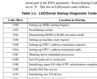
These codes are displayed on seven-segment LEDs at key points in the initialization of the hardware devices. Should the debugger fail to come up to a prompt, the last code displayed will indicate how far the initialization sequence had progressed before stalling. The serial port version of the startup codes is enabled by an ENV parameter:
Serial Startup Code Master Enable [Y/N]=N?
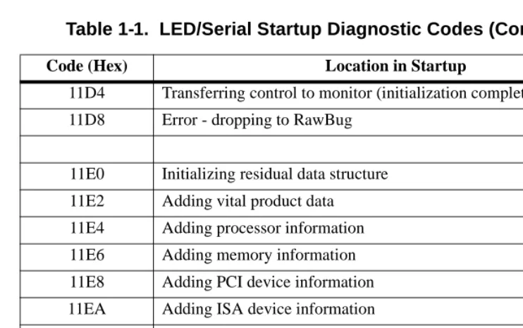
Under normal conditions, the startup sequence begins at 0x1100 and continues to the PPC1-Bug> prompt just after 0x11D4. RAM
The operating system boot sequence begins at 0x11E0 with the creation of residual data and continues to 0x11EC just before execution is passed to the boot image. The OS may have its own LED codes which are displayed after 0x11EC.
A line feed can be inserted after each serial code is displayed to prevent it from being overwritten by the next code. This is also enabled by an ENV parameter:
Serial Startup Code LF Enable [Y/N]=N?
The following firmware codes are always sent to 7-segment LEDs located at ISA I/O address 0x8C0. These codes can also be sent to the debugger serial port if the ENV parameter “Serial Startup Code Master Enable” is set to ‘Y’. The list of LED/serial codes follows.
Table 1-1. LED/Serial Startup Diagnostic Codes
Code (Hex) Location in Startup
1100 Setting up MSR (startup begins)
1102 Invalidating caches
1104 Determining ROM or RAM execution mode
1106 Setting up machine state register
1108 Setting up CPU’s address translation registers
110A Setting up CPU’s address translation table
110C Shutting down redundant processors
110D Init I/O path out to serial port
110E Initializing super I/O chip (CPU initialization completed)
110F Enable ISA bus access
1110 Initializing raw I/O device
1111 Initialize early stack memory
1112 Getting PHB (PCI Host Bridge) Table Pointer
1113 Disable all caches
1114 Initializing PCI bridge
1116 Initializing the powerup flag indicator
111A Waiting for hardware to initialize memory
111C Setting up the DRAM init parameters
111E Initializing DRAM in bridge/memory controller
1120 Setting up debugger memory page area
1122 Calculating and setting DRAM speed
1124 Calculating and setting ROM speed
1126 Enabling instruction cache
1128 Setting up debugger memory page tables
112A Setting up debugger kernel pointers and saving registers
112B Setup the exception control description
112C Setting up buginit section pointers and runtime variables
1130 Retrieving the processor board type
1132 Initializing the Z8536
1134 Initializing local board status
1136 Retrieving the base board type
1138 Checking the level of the ABORT push-button
113A Initializing the interrupt/timer controller
113C Retrieving MPU identifier
113E Enabling super-scalar modes
1140 Adding processor-specific work-arounds
1142 Getting the bus clock speed
1144 Initializing the keyboard controller
1145 Probe for PCI functions
1146 Initializing the PCI interrupt route control registers
1148 Starting PCI hierarchy configuration process
12nn Probing PCI config space (nn = bbbddddd; bbb = bus#, ddddd = dev# Table 1-1. LED/Serial Startup Diagnostic Codes (Continued)
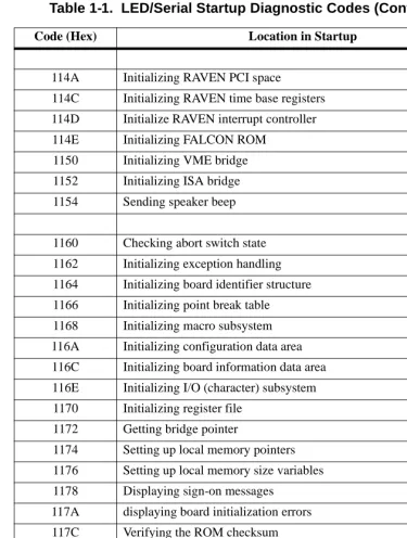
114A Initializing RAVEN PCI space
114C Initializing RAVEN time base registers
114D Initialize RAVEN interrupt controller
114E Initializing FALCON ROM
1150 Initializing VME bridge
1152 Initializing ISA bridge
1154 Sending speaker beep
1160 Checking abort switch state
1162 Initializing exception handling
1164 Initializing board identifier structure
1166 Initializing point break table
1168 Initializing macro subsystem
116A Initializing configuration data area
116C Initializing board information data area
116E Initializing I/O (character) subsystem
1170 Initializing register file
1172 Getting bridge pointer
1174 Setting up local memory pointers
1176 Setting up local memory size variables
1178 Displaying sign-on messages
117A displaying board initialization errors
117C Verifying the ROM checksum
117E Displaying memory size and misc errors
1180 Displaying MPU clock speed
1182 Verifying MPU clock speed
1184 Displaying bus clock speed
1186 Initializing network I/O subsystem
Table 1-1. LED/Serial Startup Diagnostic Codes (Continued)
1188 Initializing disk I/O subsystem
118A Initializing direction flags
118C Initializing NVRAM (PReP) environment
118E Initializing residual data pointer
1190 Initializing input/output pointers
1192 Initializing diagnostic subsystem
1194 Setting up special init section pointers and runtime variables
1196 Initializing abort switch
1198 Setting up board suffix and return environment
11A0 Retrieving the processor board type
11A2 Displaying memory warning and MPU configuration
11A4 Clearing MPU idle semaphores
11A6 Waiting for MPU logins
11A8 Displaying MPU status information
11AA Setting up DRAM and bridge pointers
11AC Initializing DRAM ECC/parity
11AE Displaying DRAM information
11B0 Setting up misc. L2 cache variables
11B2 Setting up L2 cache size variables
11B4 Initializing and flushing L2 cache data parity
11B6 Displaying L2 cache parity state
11B8 Reading NVRAM contents
11BA Verifying NVRAM header
11BC Initializing NVRAM contents
11BE Retrieving global environment variable pointers
11D0 Initializing processor timebase/decrementer registers
Table 1-1. LED/Serial Startup Diagnostic Codes (Continued)
Running the Diagnostics and Debugger
In order to use the diagnostics, terminate the start-up process by pressing ESC or the Break key during one of the four pauses (PowerPlus
architecture boards in their default configuration may not pause at any of the four places.) The diagnostics prompt (PPCx-Diag>) appears. You may switch to the debugger prompt (PPCx-Bug>) by using the SD command.
Both the debugger and diagnostic commands are available from the diagnostic prompt. Only the debugger commands are available from the debugger prompt.
You may view a list of the diagnostics or debugger commands by using the
HE (Help) command.
Note Some diagnostics depend on restart defaults that are set up only in a particular restart mode. Refer to the PPCBug Diagnostics Manual, PPCDIAA/UM, for the correct mode.
11D4 Transferring control to monitor (initialization complete)
11D8 Error - dropping to RawBug
11E0 Initializing residual data structure
11E2 Adding vital product data
11E4 Adding processor information
11E6 Adding memory information
11E8 Adding PCI device information
11EA Adding ISA device information
11EC Residual data completed
12nn Probing PCI config space (board specific)
Table 1-1. LED/Serial Startup Diagnostic Codes (Continued)
Refer to the PPCBug Diagnostics Manual for complete descriptions of the diagnostic routines available and instructions on how to invoke them.
Auto Boot
Note The PowerPlus architecture boards do not execute a configured boot routine.
Auto Boot is the default boot routine. It provides an independent mechanism for booting an operating system. No console is required. Autoboot selects the boot device from either a scan list of device types, a floppy diskette, a CD-ROM, tape, or a hard disk.
You may change the scan order, or configure Auto Boot to boot from a specific Controller Logical Unit Number (CLUN) and Device Logical Unit Number (DLUN) by changing the ENV command parameters for enabling Auto Boot (refer to Chapter 3, for information).
At power-up, Auto Boot is enabled. The following message is displayed on the system console:
Autoboot in progress... To abort hit <BREAK>
Following this message there is a delay to allow you to abort the Auto Boot process and gain control. Press either the BREAK key or the software abort or reset switch to abort Autoboot.
If you do not abort Auto Boot, the actual I/O is begun. The program pointed to within the boot-record of the media specified is loaded into RAM, and control is passed to it.
ROMboot
Note The PowerPlus architecture boards do not execute a configured boot routine.
ROMboot is a mechanism for booting an operating system from a user-defined routine stored in ROM. ROMboot executes at power-up (or optionally at reset) if it is configured and enabled in parameters set with the ENV command. It may also be executed with the RB (ROMboot) command.
Refer to Chapter 3, for information on setting the ENV command parameters for enabling ROMboot.
For ROMboot to work, a ROMboot routine must be stored in the FLASH memory to support it. If ROMboot code is installed, a user-written routine is given control (if the routine meets the format requirements). One use of ROMboot might be resetting SYSFAIL* on an unintelligent controller board.
The NORB command disables ROMboot.
For a user’s ROMboot routine to gain control through the ROMboot linkage, four requirements must be met:
❏ Power must have just been applied (or at reset, if configured to do so with the ENV command).
❏ Your ROMboot routine must be stored within the PowerPC board FLASH memory map (or elsewhere in onboard memory, if configured to do so with the ENV command).
❏ The ASCII string “BOOT” must be located within the specified memory range.
❏ Your ROMboot routine must pass a checksum test, which ensures that this routine was really intended to receive control at power-up.
The format of the beginning of the routine is:
If you want to make use of ROMboot, you do not have to fill a complete FLASH device. Any partial amount is acceptable, as long as:
❏ The identifier string “BOOT” starts on a word (FLASH and Direct spaces) or 8KB (local RAM and VMEbus spaces) boundary.
❏ The ROMboot routine size (in bytes) is evenly divisible by 2.
❏ The length parameter (offset $8) reflects where the checksum is, and the checksum is correct.
ROMboot searches predefined areas of the memory map for possible routines and checks for the “BOOT” indicator. Two events are of interest for any location being tested:
❏ The map is searched for the ASCII string “BOOT”.
❏ If the ASCII string “BOOT” is found, it is still undetermined whether the routine is meant to gain control at power-up or reset. To verify that this is the case, the bytes starting from “BOOT” through the end of the routine, excluding the two byte checksum, are run through the debugger checksum algorithm. If the result of the checksum is equal to the final two bytes of the ROMboot routine (the checksum), it is established that the routine was meant to be used for ROMboot.
Under control of the ENV command, the sequence of searches is as
Offset Length Contents Description
$00 4 bytes BOOT ASCII string indicating possible routine; the checksum must be valid
$04 4 bytes Entry Address Word offset from “BOOT”
$08 4 bytes Routine Length Word; includes length from “BOOT” to and including a two-byte checksum
$0C Length of name
1. Search direct address for “BOOT”. The direct address points to an installed ROMboot routine. It is a variable that may be set using the
ENV command.
2. Search complete ROM map.
3. Search local RAM, at all 8KB boundaries starting at the beginning of local RAM.
4. Search the VMEbus map (if so selected by the ENV command) on all 8KB boundaries starting at the end of the onboard RAM. VMEbus address space is searched both below (if the start address of local RAM is not located at 0) and above local RAM up to the beginning of FLASH Space.
Sample ROMboot Routine
The example ROMboot routine performs the following:
❏ Outputs a <CR> <LF> sequence to the default output port.
❏ Displays the date and time from the current cursor position.
❏ Outputs two more <CR> <LF> sequences to the default output port.
8. Verify the functionality of the user ROMboot routine with the RB command.
PPC1-Bug>RB; V <Return>
ROMboot about to Begin... Press <ESC> to Bypass, <SPC> to Continue Direct Add: FFC00000 FFFFFFFC: Searching for ROMboot Module at: 00010000 Executing ROMboot Module “TEST” at 00010000
MON MAR 27 10:39:08.00 1995
PPC1-Bug>
The sample ROMboot routine is now ready for use.
Network Auto Boot
Network Auto Boot (or Network Boot) is a software routine that provides a mechanism for booting an operating system using an Ethernet network as the boot device.
Network Auto Boot executes at power-up (or optionally at reset) if it is configured and enabled in parameters set with the ENV command.
This routine selects the boot device based on the Controller Logical Unit Number (CLUN) and Device Logical Unit Number (DLUN) which have been set in the ENV command.
Refer to Chapter 3, for information on setting the ENV command parameters for enabling Network Auto Boot.
If Network Boot is enabled, the following message is displayed on the system console at power-up:
Network Boot in progress... To abort hit <BREAK>
Following this message there is approximately a five-second delay before the actual I/O is begun. The program pointed to within the volume ID of the media specified is loaded into RAM and control is passed to it.
Network Autoboot is controlled by parameters contained in the NIOT and
ENV commands. These parameters allow the selection of specific boot
devices, systems, and files and allow programming of the boot delay. Refer to the NIOT and ENV commands in Chapter 3, for more details.
Restarting the System
You can initialize the system to a known state in three different ways: reset, abort, and break. Each has characteristics which make it more appropriate than the others in certain situations.
Reset
Pressing and releasing the board front panel RESET switch initiates a system reset. Cold and warm reset modes are available. By default, PPCBug is in cold mode (refer to the RESET command description in Chapter 3). During cold reset, a total system initialization takes place, as if the PowerPC board had just been powered up. All static variables are restored to their default states. The breakpoint table and offset registers are cleared. The target registers are invalidated. Input and output character queues are cleared. Onboard devices are reset, and the first two serial ports are reconfigured to their default state.
During warm reset, the PPCBug variables and tables are preserved, as well as the target state registers and breakpoints.
Reset must be used if the processor ever halts, or if the PPCBug environment is ever lost, such as if the vector table is destroyed, or the stack is corrupted.
Abort
this reason, abort is most appropriate when terminating a user program that is being debugged. Abort should be used to regain control if the program gets caught in a loop. The target IP and register contents help to pinpoint the malfunction.
Pressing and releasing the ABORT switch generates a local board condition which interrupts the microprocessor. The target registers, reflecting the machine state at the time the abort switch was pressed, are displayed on the screen. Any breakpoints installed in the user code are removed, and the breakpoint table remains intact. Control is returned to the debugger.
Reset/Abort
You may wish to perform “double-button reset” by pressing the RESET and ABORT switches at the same time. Release RESET first, wait seven seconds, and then release ABORT. This resets all onboard devices, as well as sending a SYSRESET* signal if the board is the VMEbus system controller. It also ignores the parameters stored in NVRAM, and starts debugger execution with the same ENV parameters as if you had used the command ENV;D.
Break
A break is generated by pressing and releasing the BREAK key on the current-console keyboard. Break does not generate an interrupt. The only time break is recognized is when characters are sent or received by the console port. Break removes any breakpoints in the user code and keeps the breakpoint table intact. Break also takes a snapshot of the machine state if the function was entered using SYSCALL. This machine state is then accessible to you for diagnostic purposes.
Board Failure
The following conditions result in a board failure. These conditions also give a WARNING message, if possible:
❏ Board initialization error/failure
❏ Debugger object checksum error
❏ Configuration data (NVRAM ENV parameters) failure (i.e., checksum)
❏ Configuration data (NVRAM CNFG parameters) failure (i.e., checksum)
❏ Calculated MPU clock speed does not match the associative CNFG parameter
❏ Calculated BUS clock speed does not match the associative CNFG parameter
❏ Selftest error/failure
If the board is equipped with a board fail LED, the LED will be illuminated when a board failure occurs.
SYSFAIL* Assertion and Negation (VMEbus Boards)
On VMEbus boards, the board fail is the same as the SYSFAIL indicator. At reset or power-up, the debugger asserts the VMEbus SYSFAIL* line (refer to the VMEbus specification).
The SYSFAIL* line is negated if debugger initialization is done and if none of the board failure conditions have occurred. However, SYSFAIL* stays asserted if any of the board failure conditions have occurred. In this way, the state of the debugger is indicated to the user or VMEbus masters. In a multi-computer configuration, other VMEbus masters could view the pertinent control and status registers to determine which CPU is asserting SYSFAIL* in the event of a board failure.
Notes Assert indicates a signal is active or true. Negate indicates a signal is inactive or false. These terms are used
independently of the voltage levels (high or low) that they represent.
The asterisk (*) in the signal name SYSFAIL* denotes that the signal is true or valid when the it is low (SYSFAIL* is level sensitive).
MPU Clock Speed Calculation
The MPU clock speed is calculated and checked against the MPU clock speed parameter located in NVRAM, which you may set in the CNFG
command. If the check fails, a warning message is displayed. The calculated clock speed is also checked against known clock speeds and tolerances.
Refer to Chapter 3, for information on setting the CNFG command parameters.
Disk I/O Support
The debugger can initiate disk input and output by communicating with intelligent disk controllers over the PCI bus. Disk support facilities built into the debugger consist of command-level disk operations, disk I/O system calls (only via one of the system call instructions) for use by user programs, and defined data structures for disk parameters (refer to Chapter 5, System Calls for information on system calls).
Parameters such as the address where the module is mapped and the type and number of devices attached to the controller module are kept in tables by PPCBug. Default values for these parameters are assigned at power-up and cold-start reset, but may be altered as described in Default PPCBug Controller and Device Parameters on page 1-27.
Blocks and Sectors
The logical block defines the unit of information for disk devices. A disk is viewed by PPCBug as a storage area divided into logical blocks. By default, the logical block size is set to 256 bytes for every block device in the system. The block size can be changed on a per device basis with the
IOT command.
The sector defines the unit of information for the media itself, as viewed by the controller. The sector size varies for different controllers, and the value for a specific device can be displayed and changed with the IOT command.
When a disk transfer is requested, the start and size of the transfer is specified in blocks. PPCBug translates this into an equivalent sector specification, which is then passed on to the controller to initiate the transfer. If the conversion from blocks to sectors yields a fractional sector count, an error is returned and no data is transferred.
Device Probe
A device probe with entry into the device descriptor table is done
whenever a specified device is accessed. This happens when system calls .DSKRD, .DSKWR, .DSKCFIG, .DSKFMT, and .DSKCTRL, and commands IOC, IOP, IOT, MAR, MAW, and PBOOT are used.
The device probe mechanism utilizes the SCSI commands Inquiry and
Mode Sense. If the specified controller is non-SCSI, the probe simply
returns a status of device present and unknown. The device probe makes an entry into the device descriptor table with the pertinent data. After an entry has been made, the next time a probe is done it simply returns with
Disk I/O via Debugger Commands
The following debugger commands are provided for disk I/O. Refer to
Chapter 3, for instructions for their use. When a command is issued to a particular controller LUN and device LUN, these LUNs are remembered in the debugger so that the next disk command uses the same controller and device.
IOI (Input/Output Inquiry)
The IOI command is used to probe the system for all possible
CLUN/DLUN combinations and display inquiry data for devices which support it. The device descriptor table only has space for 16 device descriptors. With the IOI command, you can view the table and clear it if necessary.
IOP (Physical I/O to Disk)
!
CautionIf you start the IOP format procedure, it must be allowed to complete (PPCxBug> prompt returns) or else the disk drive may be totally disabled. This format procedure may take as long as half an hour.
The IOP command allows you to read or write blocks of data, or to format the specified device in a certain way. IOP creates a command packet from the arguments you specify, and then invokes the proper system call function to carry out the operation.
IOT (I/O Configure)
The IOT command allows you to change any configurable parameters and attributes of the device. In addition, it allows you to see the controllers available in the system.
IOC (I/O Control)
PBOOT (Bootstrap Operating System)
The PBOOT command reads an operating system or control program from the specified device into memory, and then transfers control to it.
controller it is sent to. Refer to documentation on the particular controller module for the format of its packets. Refer to the IOC command section in
Chapter 3, Debugger Commands for information on sending command packets.
Default PPCBug Controller and Device Parameters
PPCBug initializes the parameter tables for a default configuration of controllers (refer to Appendix E, Disk and Tape Controllers). If the system needs to be configured differently than this default configuration (for example, to use a different drive), then these tables must be changed.
Use the IOT command to reconfigure the parameter table manually for any controller and/or device that is different from the default. This is a temporary change and is overwritten if a cold-start reset occurs.
Disk I/O Error Codes
PPCBug returns an error code if an attempted disk operation is
Network I/O Support
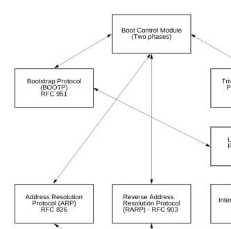
The network autoboot firmware provides the capability to boot the CPU through the ROM debugger using a network (local Ethernet interface) as the boot device.
The booting process is executed in two distinct phases.
❏ The first phase allows the diskless remote node to discover its network identify and the name of the file to be booted.
❏ The second phase has the diskless remote node reading the boot file across the network into its memory.
Figure 1-1 on page 1-29 depicts the various modules (capabilities) and the dependencies of these modules that support the overall network boot function. They are described in the following paragraphs.
Physical Layer Manager Ethernet Driver
This driver surrounds and manages the Ethernet controller chip or module. Management includes the reception of packets, the transmission of packets, flushing of the receive buffer, and interface initialization.
This module ensures that the packaging and unpackaging of Ethernet packets is done correctly in the Boot PROM.
UDP and IP Modules
The Internet Protocol (IP) is designed for use in interconnected systems of packet-switched computer communication networks. The Internet Protocol provides for transmitting blocks of data called datagrams (hence User Datagram Protocol, or UDP) from sources to destinations, where sources and destinations are hosts identified by fixed length addresses.
Figure 1-1. Network Boot Modules
1273 9401
Bootstrap Protocol (BOOTP) RFC 951
Boot Control Module (Two phases)
Trivial File Transfer Protocol (TFTP)
RFC 783
User Datagram Protocol (UDP)
RFC 768
Internet Protocol (IP) RFC 791 Reverse Address
Resolution Protocol (RARP) - RFC 903 Address Resolution
Protocol (ARP) RFC 826
Ethernet Driver Physical Layer
RARP and ARP Modules
The Reverse Address Resolution Protocol (RARP) basically consists of an identity-less node that broadcasts a “whoami” packet onto the Ethernet and waits for an answer. The RARP server fills an Ethernet reply packet up with the target's Internet Address and sends it.
The Address Resolution Protocol (ARP) basically provides a method of converting protocol addresses (e.g., IP addresses) to local area network addresses (e.g., Ethernet addresses). The RARP protocol module supports systems which do not support the BOOTP protocol (refer to BOOTP Module below).
BOOTP Module
The Bootstrap Protocol (BOOTP) basically allows a diskless client machine to discover its own IP address, the address of a server host, and the name of a file to be loaded into memory and executed.
TFTP Module
The Trivial File Transfer Protocol (TFTP) is a simple protocol to transfer files. It is implemented on top of the Internet User Datagram Protocol (UDP or Datagram) so it may be used to move files between machines on different networks implementing UDP. The only thing it can do is read and write files from/to a remote server.
Network Boot Control Module
Network I/O Error Codes
PPCBug returns an error code if an attempted network operation is unsuccessful. Refer to Appendix H, Network Communication Status
Codes for an explanation of network I/O error codes.
Multiprocessor Support (Remote Start)
PPCBug can be configured to monitor a dual-ported resource and, upon receipt of a certain ‘signal’, pass program control to (that is, commence execution at) a user specified address.
Note PCI Remote Start is only supported on boards equipped with the DEC2155x PCI-to-PCI Bridge device.
A dual-ported resource is a hardware feature that makes local memory locations or registers available to remote processors as well as to the local processor.
This ‘remote start’ capability is provided to allow the user to take advantage of boards with dual-ported resources to implement and “bootstrap” a multiprocessor system where member processor boards can be tightly coupled via an interface such as the VME bus.
PPCBug remote start can be utilized by either the MPCR or GCSR methods, which are described in the next subsections. Either or both methods can be enabled or disabled in the non-volatile PPCBug
configuration by the ENV command. The name of this ENV parameter is “Remote Start Method Switch”. The valid choices for this parameter are:
Multiprocessor Control Register (MPCR) Method
The MPCR method of remote start is based on the use of dual-ported local memory resources.
A remote processor board (the host) can initiate PPCBug functions on the target processor board by issuing commands through the remote start memory interface. The target processor board is the one executing PPCBug, out of its local (on-board) resources.
The remote start memory interface is implemented using two contiguous words of local memory, defined as the Multiprocessor Control Register (MPCR), and Multiprocessor Address Register (MPAR).
The local address of MPCR is fixed, within PPCBug’s reserved memory area which is located in the topmost portion of local RAM. This address can be calculated as <the local RAM size (in bytes)>-$1C000.
Note: Care should be taken not to write to memory locations
adjacent to the MPCR and MPAR as this could cause corruption of PPCBug internal variables and vector tables, resulting in possible PPCBug malfunction.
ENV Parameter
Value
Remote Start Method Setting
G GCSR method only
M MPCR method only
B both GCSR and MPCR methods active
The host’s access address of the MPCR is affected by memory mapping which is configured by the user and must be calculated accordingly.
The MPCR consists of two words used to control communication between processors. It is organized as follows:
The status codes stored in the MPCR command/status byte are of two types:
❏ Status returned from PPCBug (the target processor)
❏ Status set (by the host processor)
The MPCR status codes that may be written to this location by PPCBug (the target processor) are:
Table 1-2. MPCR Method Remote Start Register Model
Register Name
Byte Offset
31 30 29 28 27 26 25 24 23 22 21 20 19 18 17 16 15 14 13 12 11 10 9 8 7 6 5 4 3 2 1 0
MPCR 0 Command
/Status Reserved
MPAR 4 Address
ASCII Value
Hex Value
Indicated Status
0 ($00) Wait. PPCBug initialization is not yet complete.
‘E’ ($45) The program pointed to by the MPAR address is executing.
‘R’ ($52)
In either sequence, an E is placed in the MPCR to indicate that execution is underway just before control is passed to RAM. (Any remote processor could examine the MPCR contents.)
If the code being executed in dual-port RAM is to re-enter PPCBug, a system call using function $0063 (SYSCALL .RETURN) returns control to PPCBug with a new display prompt. Note that every time PPCBug returns to the prompt, an R is moved into the MPCR to indicate that control can be transferred once again to a specified RAM location.
GCSR Method
PPCBug supports the GCSR method of remote start, over the VMEbus, on boards equipped with the Universe PCI to VMEbus bridge.
When PPCBug is executing on the target processor board, a host processor board may initiate program execution by the target board’s MPU using the GCSR method of remote start.
This method of remote start is implemented through the dual-ported register interface provided by the Universe MBOX registers. This interface is located at offset of $348 from the base address of the Universe CSR. The GCSR register model and its offset within the Universe CSR is the same regardless of which bus (VME or PCI) it is accessed from.
The GCSR method remote start register model is organized as shown in the following table:
Table 1-3. GCSR Method Remote Start Register Model
Universe Register Name
Byte Offset
31 30 29 28 27 26 25 24 23 22 21 20 19 18 17 16 15 14 13 12 11 10 9 8 7 6 5 4 3 2 1 0
MBOX0 $348 LM/SIG
Register Reserved GCSR0
MBOX1 $34C GCSR1 GCSR2
MBOX2 $350 GCSR3 GCSR4
The LM/SIG register is assigned the following bit definitions:
The VME host board can initiate program execution by the target board’s MPU by issuing a remote GO command using the GCSR registers. The result is equivalent to the MPCR method (using command code B) described in a previous section.
The target board GO command is invoked by the VME host with the following sequence:
❏ The remote processor places the execution address for the target board MPU in general purpose registers 0 and 1 (GPCSR0=MS 16 bits, GPCSR1=LS 16 bits)
❏ The remote processor sets bit SIG0 of the LM/SIG register.
❏ The PPCBug firmware which is executing on the host board will clear SIG0, install breakpoints, and begin execution at the specified address.
Note: The above steps assume that the Universe CSR has been mapped to
the VME address space so the host may access the Universe mailbox registers. The recommended method of mapping the Universe CSR is to configure the desired address and attributes with PPCBug’s ENV
command. The ENV command parameter identifiers for this are “VMEbus Register Access Image Control Register“ and “VMEbus Register Access Image Base Address Register“. For specific programming values, refer to the UniverseII User Manual, available from Tundra Semiconductor Corporation.
Table 1-4. LM/SIG Register Bit Assignments
Data and Address Sizes
Data and address sizes are defined as follows:
A byte is eight bits, numbered 0 through 7, with bit 0 being the least significant.
A half-word is 16 bits, numbered 0 through 15, with bit 0 being the least significant.
A word is 32 bits, numbered 0 through 31, with bit 0 being the least significant.
Byte Ordering
2
Entering Commands
The debugger is command-driven and performs its various operations in response to commands that you enter at the keyboard. When the PPCx-Bug> prompt appears on the screen, the debugger is ready to accept commands.
What you enter is stored in an internal buffer. Execution begins only after you press the Return key, allowing you to correct entry errors, if necessary, using the control characters (refer to Control Characters on page 2-6). After the debugger executes the command, the prompt reappears.
However, if the command causes execution of target code (for example
GO) then control may or may not return to the debugger, depending on
what the program does. For example, if a breakpoint has been specified, then control returns to the debugger when the breakpoint is encountered during execution of the user program. For more about this, refer to the GD,
GO, and GT command descriptions in Chapter 3, Debugger Commands.
Alternately, the user program could return to the debugger by means of the System Call Handler routine .RETURN (refer to Chapter 5, System Calls).
Command Syntax
A debugger command is made up of the following parts:
❏ The command name
❏ Any required arguments, delineated with either a space or comma (precede the first argument with a space)
❏ Any required options. Precede an option or a string of options with a semi-colon (;). If no option is selected, the default options are used.
2
Command Arguments
The following arguments are common to many of the commands. Additional arguments are defined in the description of the particular command in which they occur.
Use either a space or a comma as a delimiter between arguments. You may select the default value for an argument by inserting a pair of commas in place of the argument.
EXP
The EXP (expression) argument can be one or more numeric values separated by the arithmetic operators:
EXP Expression (refer to EXP below)
ADDR Address (refer to ADDR on page 2-4)
COUNT Count; this is a numeric expression and has the same syntax as EXP (refer to EXP below)
RANGE A range of memory addresses specified with a pair of arguments, either ADDR ADDR or ADDR : COUNT
TEXT An ASCII string of up to 255 characters, delimited at each end by the single quote mark (’)
PORT Port Number (refer to PORT on page 2-6)
+ plus
- minus
2
Numeric values may be expressed in either hexadecimal, decimal, octal, or binary by immediately preceding them with the proper base identifier.
If no base identifier is specified, then the numeric value is assumed to be hexadecimal.
A numeric value may also be expressed as a string literal of up to four characters. The string literal must begin and end with the single quote mark (’). The numeric value is interpreted as the concatenation of the ASCII values of the characters. This value is right-justified, as any other numeric value would be.
Evaluation of an expression is always from left to right unless parentheses are used to group part of the expression. There is no operator precedence. Subexpressions within parentheses are evaluated first. Nested
parenthetical subexpressions are evaluated from the inside out.
Valid expression examples:
Data Type Base Identifier Example
Integer Hexadecimal $ $FFFFFFFF
Integer Decimal & &1974, &10-&4
Integer Octal @ @456
Integer Binary % %1000110
String Literal Numeric Value (Hexadecimal)
’A’ 41
’ABC’ 414243
’TEST’ 54455354
Expression Result (Hex)
FF0011 FF0011
45+99 DE
&45+&99 90
2
The total value of the expression must be between 0 and $FFFFFFFF.
ADDR
The syntax for the ADDR argument is similar to the syntax accepted by the PowerPC one-line assembler. All control addressing modes are allowed. Refer to Addressing Modes in Chapter 4, One-Line Assembler/
Disassembler.
ADDR may also be specified in the address + offset form.
ADDR Formats
The ADDR format is:
HexadecimalNumber {[^S]|[^s]|[^U]|[^u]}|Rn
Enter ADDR as a hexadecimal number (e.g., 20000 for address
$00020000). The address, or starting address of a range, can be qualified by a suffix, either ^S or ^s for supervisor address space, or ^U or ^u for user address space. The default, when the suffix is not specified, is supervisor.
Once a qualifier has been entered, it remains valid for all addresses entered for that command sequence, until either the debugger is reentered or another qualifier is provided.
In the alternate register number (Rn) form, the debugger uses the address contained in MPU Register Rn, where n is 0 through 31 (i.e., 0, 1, . . . 31).
%10011110+%1001 A7
88<<4 880
AA&F0 A0
<< represents shift-left & represents logical AND
2
If the address range specified as ADDR ADDR, with a size option of either
H (half-word) or W (word), data at the second (ending) address is acted on
only if the second address is a proper boundary for a half-word or word. Otherwise, the range is truncated so that the last byte acted upon is at an address that is a proper boundary.
Offset Registers
Eight pseudo-registers (Z0-Z7) called offset registers are used to simplify the debugging of relocatable and position-independent modules. The listing files in these types of programs usually start at an address (normally 0) that is not the one at which they are loaded, so it is harder to correlate addresses in the listing with addresses in the loaded program. The offset registers solve this problem by taking into account this difference and forcing the display of addresses in a relative address+offset format. Offset registers have adjustable ranges and may even have overlapping ranges. The range for each offset register is set by two addresses, base and top, both of which are standard in a given 64-bit offset register. Specifying the base and top addresses for an offset register sets its range. In the event that an address falls in two or more offset registers’ ranges, the one that yields the least offset is chosen.
2
PORTThe PORT argument is the logical number of the port to be used to input or output. Valid port numbers which may be used for these commands are as follows:
Command Options
Many commands have one or more options, represented in boldface type in the command descriptions. Precede an option or a string of options with a semi-colon (;). If no option is entered, the command’s default options are used.
Control Characters
Some commands, such as CNFG, MM, or RM, allow you to edit parameter fields or the contents of registers or memory. You may use the following control characters to scroll through the listed items:
0 or 00 Terminal port 0 (console port) is used for interactive user input and output (the default), or may also be used for the graphics adapter device. This port is labeled COM1 or SER1 or DEBUG on the PowerPC board or transition module.
1 or 01 Terminal port 1 (host port) is the default for downloading, uploading, concurrent mode, and transparent modes. This port is labeled either COM2 or SER2 on the PowerPC board or transition module.
V or v Go to the next field, register, or memory location. This is the default, and remains in effect until changed by entering one of the other special characters.
^ Back up to the previous field register, or memory location. This remains in effect until changed by entering one of the other special characters.
= Re-open the same field register, or memory location.
2
You may use the following control characters for limited editing while entering commands at the PPC1-Bug> prompt:
The XON and XOFF characters in effect for the terminal port may be entered to control the output from any debugger command, if the XON/XOFF protocol is enabled (default). The characters initialized by PPCBug are (you may change them with the PF command):
Entering and Debugging Programs
There are various ways to enter a user program into system memory for execution. One way is to create the program using the
Assembler/Disassembler, entering the program one source line at a time. After each source line is entered, it is assembled and the object code is loaded to memory. Refer to Chapter 4 for information on using the PPCBug Assembler/Disassembler.
DEL Delete: move the cursor back one position and erase the character at the new cursor position. If a printer port is configured (hardcopy mode), a slash (/) character is typed along with the deleted character.
CTRL-h Performs the same function as DEL.
CTRL-x Cancel line: move the cursor to the beginning of the line. If a printer port is configured (hardcopy mode), a <CR><LF> sequence is issued along with another PPC1-Bug> prompt.
CTRL-d Redisplay the entire command line entered on the following line
CTRL-a Repeat the previous line.
This happens only at the command line. The last line entered is redisplayed but not executed. The cursor is positioned at the end of the line. You may enter the line as is or you can add more characters to it. You can edit the line by backspacing and typing over old characters.
CTRL-s Wait: halt console output (XON)
2
Another way is to download an object file from a host system. The program must be in S-record format (refer to Appendix D) and may havebeen assembled or compiled on the host system. Alternately, you may create a program using the Assembler/Disassembler, and store the program to the host using the DU command. A communication link must exist between the host system and PowerPC board port 1 (Refer to the board installation and use manual). Later, download the file from the host to PowerPC board memory with the LO command.
Once the object code has been loaded into memory, you can set breakpoints if desired and run the code or trace through it.
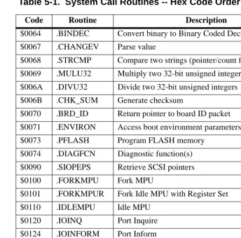
System Call Routines in User Programs
Access to various debugger routines is provided via the System Call Handler. This gives a convenient way of doing character input/output and many other useful operations so that you do not have to write these routines into the target code.
The System Call handler is accessible through the SC (system call) instruction, with exception vector $00C00 (System Call Exception).
Refer to Chapter 5, System Calls for details on the routines available and how to invoke them from within a user program.
Preserving the Operating Environment
This section explains how to avoid contaminating the operating
environment of the debugger. PPCBug uses some of the PowerPC board onboard resources to contain temporary variables and exception vectors. If the resources that PPCBug relies upon are disturbed, PPCBug may not function reliably.
2
Memory Requirements
The debugger requires approximately 768KB (maybe less) of read/write memory. It allocates this amount of memory from the top portion of memory space. For example, on a system which contains 64 megabytes ($04000000) of read/write memory (DRAM), the debugger’s memory page is located at $03F40000 to $03FFFFFF.
This memory space is used by the debugger for program stack, I/O buffers, variables, and register files. If a user program is loaded (booted, S-Records) into memory, and if this program is utilizing the debugger’s programmatic interface (i.e., system calls), the program must not modify this allocated memory.
Whenever the host hardware is reset, the target IP is initialized to $00004000 (i.e., just above the memory space of the exception vector table), and the target pseudo stack pointer is initialized to the starting location of the debugger’s read/write memory space. The target IP is set to the appropriate address if a program load operation (for example, the
PBOOT command) is initiated.
Note that user programs should handle the stack area properly in that it should not write starting at the initialized location. Some compilers and assemblers may write to the stack prior to decrementing the stack.
The amount of read/write memory space that is allocated for the debugger, and by the debugger, may increase in future releases. To properly compensate for the increased read/write memory requirements, user programs may use the target register R1 as indicator for the top (plus 1) of usable memory.
Exception Vectors
The following exception vectors are reserved for use by the debugger:
00100 - System Reset Used for the abort switch soft reset feature
00700 - Program Used for instruction breakpoints
2
These vectors may be taken over under a user’s application. However, prior to returning control to the debugger these vectors must be restored forproper operation of the affected features.
MPU Registers
Certain MPU registers must be preserved for their specific uses.
MPU Register SPR275
MPU register SPR275 is reserved for usage by the debugger. If SPR275 is to be used by the user program, it must be restored prior to using debugger resources (system calls) and or returning control to the debugger.
MPU Registers SPR272-SPR274
These MPU registers are used by the debugger as scratch registers.
Context Switching
Context switching is the switching from the debugger state to the user (target) state, or vice versa. This switching occurs upon the invocation of either the GD, GN, GO, GT, T, or TT commands, or the return from user state to the debugger state.
When the context switch transitions from the user state to the debugger state, the following MPU registers are captured:
PPC603-based boards:
R0-R31 General Purpose Registers
FR0-FR31 Floating Point Unit Data Registers
SR0-SR15 Segment Registers
SPRn Special Purpose Registers (n is 1, 8, 9, 18, 19, 22, 25, 26, 27 268, 269, 275, 282, 287, 528 - 543, 976 - 981, 1008, 1010)
IP Instruction Pointer (copy of SPR26)
2
When the context switch transitions from the debugger state to the user state, the following MPU registers are restored:
CR Condition Register
FPSCR Floating Point Status/Control Register
PPC604-based boards:
R0-R31 General Purpose Registers
FR0-FR31 Floating Point Unit Data Registers
SR0-SR15 Segment Registers
SPRn Special Purpose Registers (n is 1, 8, 9, 18, 19, 22, 25, 26, 27 268, 269, 275, 282, 287, 528 - 543, 1008, 1010, 1013, 1023)
IP Instruction Pointer (copy of SPR26)
MSR Machine State Register (copy of SPR27)
CR Condition Register
FPSCR Floating Point Status/Control Register
PPC603-based boards:
R0-R31 General Purpose Registers
FR0-FR31 Floating Point Unit Data Registers
SPRn Special Purpose Registers (n is 1, 8, 9, 275, 1010)
IP Instruction Pointer, copied to SPR26
MSR Machine State Register, copied to SPR27
CR Condition Register
FPSCR Floating Point Status/Control Register
PPC604-based boards:
0-R31 General Purpose Registers
FR0-FR31 Floating Point Unit Data Registers
2
Note that on a restoration context switch, registers whose perspectives feature MMU characteristics and operating modes of the MPU are not restored. The debugger honors the user’s MMU configuration. If the user’s program wishes to utilize the programmatic interface (i.e., system calls) of the debugger, it must maintain the address translation of 1 to 1, and the I/O resources utilized by the debugger must be data cache inhibited.
Floating Point Support
The MD and MM commands allow display and modification of floating point data in memory. Use either the MD command or the MM command to assemble or disassemble floating point instructions.
Valid data types that can be used when modifying a floating point data register or a floating point memory location:
When entering data in single or double precision format, observe the following rules:
❏ The sign field is the first field and is a binary field. IP Instruction Pointer, copied to SPR26 MSR Machine State Register, copied to SPR27
CR Condition Register
FPSCR Fl