IJSRR, 8(2) April. – June., 2019 Page 1633
Research article Available online www.ijsrr.org
ISSN: 2279–0543
International Journal of Scientific Research and Reviews
Evolution of Amorphous-Si , CIGS and CdTe Solar Thin Films With a
Comparative Market Analysis and Reliability Measures
Karthikeyan S
1*and Thirunavukkarasu P
21*
Department of Electronics, Sri Ramakrishna Mission Vidyalaya College of Arts and Science, Coimbatore-641020,Tamilnadu, India. Email:[email protected]
2
Department of Electronics, Sri Ramakrishna Mission Vidyalaya College of Arts and Science, Coimbatore-641020,Tamilnadu, India. Email: [email protected]
ABSTRACT
The current paper gives the prominent reviews of three important thin film solar technologies,
namely Amorphous silicon (α-Si), Copper indium gallium selenide (CIGS) and Cadmium telluride (CdTe). Also discussed, the way these technologies are evolved based on their hold in the market and
the reliability. The α-Si technology has almost been wiped out from the applications in terrestrial areas and hence the other two technologies are became a major share holder in the market. Thus, the
CIGS and CdTe techniques are becoming healthy competitors for the primitive solar cells that are
crystalline. However, the duration of the existence of a thin film solar technique is a major issuefor
the exploration of the possibilities of building “An integrated PV cellsystem” that needs to be
answered, prior spending the time and money.
KEYWORDS
— Thin Films, Solar Cells, Amorphous Silicon, CdTe, CIGS, PV*Corresponding Author
Mr. Karthikeyan S
Ph.D., Research Scholar,
Department of Electronics,
Sri Ramakrishna Mission Vidyalaya College of Arts and Science,
Coimbatore - 641020,
Tamilnadu, India.
IJSRR, 8(2) April. – June., 2019 Page 1634
INTRODUCTION
In the current demand for the energy, the process of making use and utilizing the sunlight for
the production of electricity is more promising technology. However, the design and manufacturing
of such device that converts the light to electricity must be highly reliable and also to be
cost-effective compared to the other sources. Various researches have been done so far on the solar
techniques which include the wafer, thin film and the organic, in-order to achieve the adequate
reliability and the affordability. For example, the crystalline silicon seems the more promising
technology because of the usage in the market which is being used, right from the labs to the
commercial integration and also it holds about 90% of the market share. Also it has resulted the high
energy conservation due to the minimal usage of the material. Though the wafer techniques are also
high efficient, it lacks in the energy conservation as it uses more materials in this. The objective is to
effectively meet theboth the constraints, the production process in a minimal cost and the high
penetration into the market of solar power. The most common and commercialized solar cells are the
α-Si, CdTe and CIGS. The application which usesthe amorphous silicon are mainly the consumer products such as the calculators, water heaters, watches and etc.,The three common techniques can
be integrated as a BIPV (Building Integrated Photovoltaic). The important difference between these
three techniques is the direct band gap which is described in the Table 1 below. Also the table
describes the usage of the very fine thinned materials and the temperature co-efficient.
Table 1. Physical properties of three major thin film technologies
Categories α-Si CdTe CIGS
Co-efficient of Absorption 1.7442E+06 cm-1 1.1148E+ 06 cm-1 > 1E + 05 cm-1
Band Gap Direct 1.75 eV Direct 1.44 eV Direct 1.0 eV-1.6 eV
Thickness 1 μm 3-5 μm 1-2 μm
Co-efficient of Temperature -0.3%/°C -0.25%/°C -0.26%/ °C
Toxic No Cadmium No
The performance of the Wafer Technique is not as expected when the intensity of the light is
very low. The coefficient of the absorption for a thin film is lesser than its counterparts which are
crystalline materials. The α-Si is found to be less toxic in nature and also it requires a less materials when compared to the CdTe and CIGS technologies. The usage of cadmium in the CdTe techniques
has proved as more hazardous for producers as well as to the customers which limits the scope of its
commercialization eventually. As the history is closely seen that the α-Si technology had a long run in the market with the inception of this technique in the solar watches and calculators somewhere in
late 1980.The other two techniques are relatively new to the domain but have more importance when
IJSRR, 8(2) April. – June., 2019 Page 1635
thin films are taken including the α-Si, CIGS and CdTe that starts with their evolution of thin film solar cells.
EVOLUTION OF THIN FILM SOLAR CELL
A. α
-Si Solar Cell
The important and the notable feature in the α-Si is the availability of a direct gap in the material which can be used to absorb a notable portion of the sunlight in a layer of size of few
micrometers.1 However, the amorphous materials are proved to have some short orders with
dangling bonds that primarily result in the shortage of minority carriers those results in electrical
abnormality. This can be reduced by the passivation of the Hydrogen to a considerable level and
increases the length of the current carriers as well. But this process can cause degradation of light
due to the Staebler-Wronski effect.
The initial properties such as the absorption spectrum that ranges till 1.7eV have created a
stunning interest among the researchers. The additional advantages of using a α-Si:H are the cost effectiveness and a small payback time of the energy.
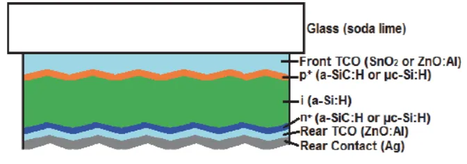
Figure 1. First Ever α-Si:H Cell
Figure 1 depicts the first ever α-Si:H cell which yielded an energy conservation of 2.4% that was developed by Carlson and Wronski.1 This is Si-H which is P-I-N nature that are deposited at a
temperature of 250 -400 degrees in a substrate of glass that are coated with the indium tin oxide
(ITO). As it could be seen from the Figure 1, there is an intrinsic layer that is thick and resides in
between the thin p-type and n-type layers that are responsible for the great lengths in diffusions for
both the minor and major carriers. The i-layer that are normally in the thickness range of 250 -
500nm usually contains little amount of boron in order to ensure the behaviour that are nearly
intrinsic when are illuminated. The layer of intransitive absorber has electric fields that are generated
and creates a separation in the electric charges and thus enabling the collection.2 In addition, the
regions that are doped (P and N) are usually very thin. The materials used for the doping are the
IJSRR, 8(2) April. – June., 2019 Page 1636
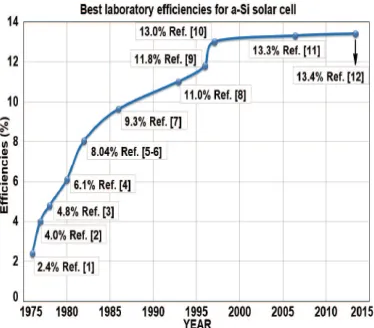
20-30 nm. Figure 2, depicts the evolution of the α-Si solar cells in the research labs that commenced
in the year 1976 when first ever α-Si was fabricated which had efficiency of mere 2.4%.1 Keeping this structure as a base, the estimation of 14-15% efficiency was made theoretically and it raised to
4% practically.2 The silicon cells with the Schottky barrier had a small and thin but with a highly
doped P-type in-between the metal and the intrinsic layer of the silicon. This had a significant
increase in the VOC and the JSC.3 Later in the year 1980, an efficiency with 6% in case of p-i-n and
6.1% in case of its counter was proved by Carlson.4
Figure 2. Evolutionary Efficiency Graph
The formal start point for the growth of α-Si was made possible after the discovery of α-Si:H in an hydrogenated formation in 1982 by Tawada et al.5,6 This had efficiency upto 8.2% and an
efficiency of 9.3 % was reported by Yamazaki et al.7 when the features of trapping the light was
introduced in the method that was developed earlier in 1992.There was more research and
development in the beginning of 1990s on the modules that are based on the many junctions(Figure
3) withhigh band gaps to allow the responses in various wavelengths. The spectrum of the solar
incorporated to a range of energy of the photons and the photons will not be observed if its energy
level less than its band gap. The provided band gap can be adjusted in the multi-junction based
technologies and the band gap will be more in the junction at the top. The energy that is subjected for
loss in a single junction cells can be obtained and converted.8An efficiency of approximately 11% is
achieved in α-Si:H cel with the concept of the multi-junction.9Later, Yang et al.contributed significantly tobring the efficiency to 13% by the process of splitting of the spectrum and using a
triple-junction.10The Improvements are seen in the Lab and achieved by the aid of two-junction and a
lower band-gap of the Si-H alloy as shown in Figure3. Further, the TCO technique ( Top Conducting
Oxide ) was developed to have the p-n junction in between the component which allows for the
transfer of the induced current and generation of electricity inside the cell in a more safer way.9,10
IJSRR, 8(2) April. – June., 2019 Page 1637
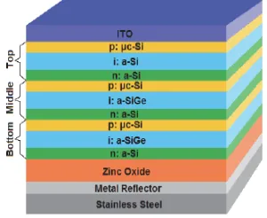
solar cell by using α-Si:H , α- SiGe:H and the microcrystalline in top, middle and bottom cells respectively.11
Figure 3. Band Gaps in Different Materials
The further technologies enhanced the efficiency significantly by using the triple junction
technology and will be explored in near future. The method of using multiple materials for
semiconducting has resulted in a border spectrum of absorption of the wavelengths and thus
improvises the conversion efficiency.
B. CIGS Solar Cells
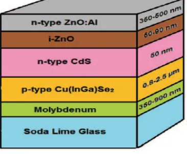
Figure 4. gives a clear idea on the evolution pattern of the CIGS in terms of the
efficiency. Kazmerski et al was the first to develop a CIGS cell with an efficiency of 4.5%. Figure5.
shows the typical structure of CIGS cell having the soda lime glass as a substrate. Molybdenum is
placed on the top of the glass that are responsible for contacting the p-type Cu(InGa)Se2. The type P
forms the main junction with n-type as CdS that acts as a layer of buffer. Out together, the size of the
cell was about is 1.2 – 4.04 μm, which are very thin when compared to the crystalline silicon which ranges from 170-200 μm in size. The enhancements made in 75% of the light to pass the initial radiation which paved the way for an efficiency of 5.7% This improvement paved a way for a better
absorbing capability with the help of carriers over a CdS window and a junction with improved
characteristics.12 Further, the parameter of the lattice was also proved to be matched with the CdS.
The efficiency was found to be below 10% due to the high resistance and the low JSC. In the year
1980 a fabrication of the CdS and CuInSe2 junction was made in a hybrid manner that gave 5.7%
efficiency with the use of a evaporation method for the deposition of CuInSe2 film.13 This achieved
IJSRR, 8(2) April. – June., 2019 Page 1638
Figure 4. Evolution of CIGS
Chen and Mickelsenmade use of the n and p type of CuInSe2 and substantially improved the
efficiency level to 7.5%. 14 The significance is its structurewhere there are adjustments made in the
selenide layers. Taking the results, the optimization was carried out in the resistivity and achieved a
10% efficiency. In the year 1981 a demonstration was made with an efficiency of 9.4 % by changing
the evaporation method of the selenide layers.15 These films are deposited with a constant In and Se
rates in decompositions and adjustments were made to the Cu to achieve the expected resistivity.
Figure 5. Structure of a CIGS Cell
The property of the transport in the hetero-junction is influenced by the concept of
recombination. The limitations of this technique was then tried to be learnt by the process of
annealinga combination of H2/Ar and pure oxygen. There was a constant improvement in the value
of the JSC owing to the thermal effect that are independent of the ambient and the VOC and FF had a
gain only in the oxygen filled area. Thus a notable increase in the efficiency was achieved.
Mickelsen and Chen made use of the mixture of ZnxCd1-xS for the improvement of the VOC and
JSC and recorded an efficiency percentage of 10.6.16 By adding Zn into the layer of sulfide has made
an increase in the VOC due to the increases of electron match affinity in-between the layers.
In 1993, Chen et al.proposed a methodology with the quaternary layer as the absorber and the
IJSRR, 8(2) April. – June., 2019 Page 1639
carriers.17 The efficiency was found to be improved over the gain in the structure due to the increase
in temperature of the substrate that was above 500 degree Celsius. With this, a total efficiency of
13.7% was achieved. In the year 1994, an efficiency of 15.9 % was reported from the solar cell that
was made from the (Inx,Ga1-x)2Se3 Further enhancement was made by sputtering the emitter ZnO
with an air-reflection coating leading to an efficiency of 17.7%.18,19 Further enhancement in the
efficiency was brought by the optimization of the ZnO layer which substantially improved the
interface in between the CIGS and the CdS layer kept in buffer. Contreras et al. made a contribution
in increasing the efficiency to 18.8%.20 In the year 2003the band gap was used with its grading in
the various concentrations of the Ga and the In for the VOC to get increases leading to an efficiency
of 19.2%.21 Contreras et al. in the year 2005, increased the efficiency to 19.5% by engineering the
band gap in the absorber.22 Inefficiency of the order of 19.9 % was produced by minimizing the
recombination and by lowering the band gap through which the VOC was made constant but the FF
shooter up to 81.2% as communicated by Contreras et al.23
The important and primary goal of the industry and the researchers is to build low-cost and
efficient solar thin films. A large sum is invested in the research directions to find the low cost
manufacturing techniques. The ZSWcontributed a lot and brought the efficiency up to 20.3% with
minimum thickness and a metal contact.24 In the year 2013, the EMPA designed and fabricated a thin
CIGS over a substrate of a polymer and produced 20.4% efficiency.25 Powalla et al. used the process
of co-evoporation and produced the same efficiency and on further investigations and experiments,
an efficiency of 20.8% was achieved by doping the potassium intentionally in the Cu(In,Ga)Se2
layer.26 This new process of doping actually paved the way for the change in the CIGS composition
into the high content of gallium without dropping the efficiency. This novel procedure of deposition
give way for the overcoming of the VOC’s saturation and change in the composition with great
content of gallium. In the year 2016, Herrmann et al. proposed a increase in the rate of distribution of
the CIGS and produced 21% efficiency.27 At last in the year 2017 an efficiency of 21.7% was
produced by Jackson et al. and it was achieved by optimizing the alkali after the deposition of the
IJSRR, 8(2) April. – June., 2019 Page 1640
C. CdTe Solar Cells
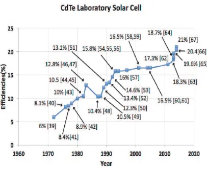
Figure 6. Evolution of CdTe
CdTe is an important material for all the solar thin films. It has a straight band gap like CIGS
that has a large coefficient of absorption. The high efficient thin film cells of CdTe are enough for
the production by curbing the surface combination. It has the stability which it has got from different
techniques. The first ever live lab for CdTe was started in the year 1972 by Bonnet and Rabnehorst
which developed a solar cell of CdTe with an efficiency of 6%. This cell was developed with a three
step process that involved very high range of temperature vapor and also very high
evaporation.29Many problems were faced by these scientists that involve the back contact in between
the Mo and the element itself, making the substrate which lead to a series of high resistances and also
low in FF.
In the year 1976, Nakayama et al. identified the screen-printing techniques in the CdTe
cells.30 The In2O3 and the CdS films that are ceramic are coated in the top of a substrate made out of
glass. This acted as a ohmic contact that are transparent to the CdTe layer and thus reducing the
resistances which yielded an efficiency of 8.1% .Bube et al hadan in-depth investigation and came
out with theCdS/CdTe heterojunction cells that produced 8.4% of efficiency. Here, the structure are
in diffusion of the donors and from the n-Cds through the p-CdTe in the process of formation of the
junction are believed to get the modified n-CdS/n-CdTe/p-CdTe junction with which the films of the
CdS are served as a role of a contact in the homo junction of the CdS. It is well seen that there is an
increase in the effective acceptance by doping the concentration of the middle to a level of 1017 cm-3
that became a significant in order to minimize the effects in terms of velocity coming through the
recombination.
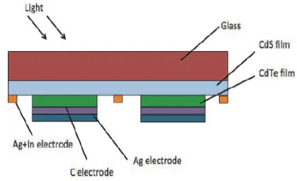
Kuribayashi introduced the electrodes that are made out of carbon in the decomposition of the
Cds and the layer of the CdTe for the enhancement of the p-type character and to ensure the allowing
IJSRR, 8(2) April. – June., 2019 Page 1641
method, the diffusion in the carbon used an approximate amount of the Cu and helped in making the
CdTe layer p+ type and made a remarkable contribution in the minimization of the resistance as
depicted in the Figure 7.
Figure 7. Structure of a CdTe Cell
1987 has a great revolution in the industry of CdTe. Ametek developed a novel design of p-i
that has various advantages over the conventional CdTe design and are able to accommodate the
innate physical properties.34 Highly efficient cells are often had a problem of high resistance that
produced films of low resistivity. Additionally, rectification rather than low resistance contacts was
utilized, and the field in the i-layer assisted in the collection of charge carriers. CdS and ZnTe are
naturally n-type and p-type materials as well. The disconnections that are minimal are used in the
valence of the edges of the CdTe interface which paved the way for the free movement of the holes.
This increased the efficiency to 10.4%. The focus of the research is deviated to the conductive layers
of the oxides as the cells are found to be more best in operation in the state of the superstrate as when
the light comes in, through the junctions that are active and the survival of all the other cells. Wu et
al. at NREL carried out their work continuously and produced efficiencies up to 16.5%. This was
made possible by the increase of the content of oxygen used and decrease of the size of the grain.
The presence of oxygen in the nano crystalline have made the inner diffusions to get
suppressed to the film and a formation of the CdS:O alloy that results in more quantum power. The
control of the inner diffusion is more important as it makes the value of FF to achieve 76% which
paved the way for the achievement of a 16% efficient. These results speculated that the presence of
CdSTe film alloy owing to the diffusion in the CdTe and the Te. This inner layer makes the
efficiency to get improved by minimizing the recombination. The complete industry was dominated
by the FSRD that reported various levels of efficiency such as 18.7%, 19.6%, 20.4%, and 21% that
had more focus on the commercialization. This uses a continuing process of manufacturing that
creates a PV module in a short time. It is observed that in the window layer, the CdS gets deposited
in the VTD first and then the CdTe is deposited, This continues for the creation of the record creating
IJSRR, 8(2) April. – June., 2019 Page 1642
MARKET SHARE
The photo voltaic industry has a 15% growth in the year 2018 from 46.0 GWp in 2017 to
50.0 GWp in the year 2018. The growth of the PV industry is so high that more than a sum of 100
new companies have step into the market which increased the production for the power summing up
to 2141 MW.36 There is an expectation that in a longer run, the PV technique will definitely surpass
the conventional crystalline methods provided the efficiency and the reliability are maintained. The
investors are also worried because of the low cost manufacture of crystalline modules with greater
efficiency which happen to be a major setback for the thin film industries. The heavy price slashes in
the crystalline cells have made the demand for the thin film cells to reduce to a considerable level.
The manufacturers are facing a market where there is a price fall that eroded many advantages of
using a PV cell and thus diminished the global demand.
In the year 2008, the thin film standard had a 14% share and was increased to 17% by the
year 2009. Then there was a substantial decrease in the value of the market share and came down to
6-8% in the year 2014.37 The cost factor was a major hindrance for the PV manufacturers which
made the market value go down drastically and could not compete with the low cost crystalline
techniques that are followed in the neighbouring countries where the cost of manufacturing are low.
In the entry time, the, α-Si grew at a rapid rate of 30% annually but as of the current scenario, it has only less than 1% of the global market value. Possibilities of these to re-enter the market are in
applications for space where these have an important advantage of giving less mass and less damages
caused due to radiations. The listed consequences in the staebler- wronski effects will not be a
hindrance as it is opposed in the operation in terrestrial region. Also, the focus now is on the ways to
integrate the microcrystalline with the amorphous composition mixes which have promising
outcomes.
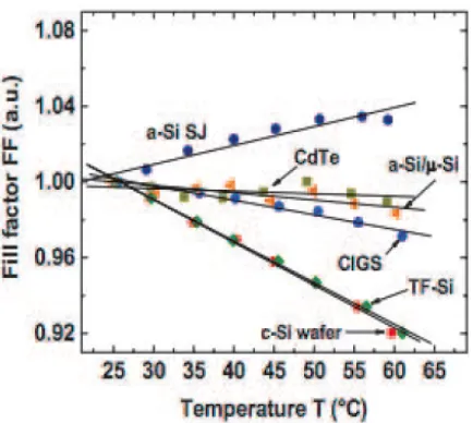
RELIABILITY
The reliability of a thin film PV cell is always questionable when compared to the crystalline
structures. As far as the performance is considered, it is understood that the power loss owing to the
operating temperature varies based on the type of film used since it has a range of coefficients for the
temperature. For instance, the induced light defects may have a more privilege in the α-Si thin film owing to the fact of the degradation of the material due to the Staebler-Wronski effect. The effect’s
strength is directly related with the structure of the device as it has very thin intrinsic layer that
shows a low performance loss due to the recombination that are decreases in the photo carriers.
Figure 8. Depicts the effects that the temperature has on the FF of the three thin film techniques
IJSRR, 8(2) April. – June., 2019 Page 1643
behavior as with the rise in temperature. The exception in case of α-Si is due to the effect of Staebler-Wronski where there is a regenerative and the effect that incurs benefits are occurring
owing to the annealing. The research on the coefficients of the temperature is highly essential as it
determines the size and design of a photo-voltaic cell. Many of the recent manufacturers particularly
“First Solar” have collaborations with the NREL for more learning on the prospect of reliability in
the commercial sectors.
Figure 8. Temperature Vs Fill Factor
CONCLUSION
The α-Si owing to its less efficiency and the instability can be used only for the niche applications of the consumers. The less efficiency of the amorphous silicon is due to the dangling
bonds and the materials that resulted in the short length of diffusion in carrying the minorities. The
effect of Staebler-Wronski also causes the efficiency to be not in stable. The discovery of a
hydrogenated α- Si:H increases the efficiency to 8.04% which is still not sufficient for the power generation for kilowatt requirements in the terrestrial areas. Then the concept of using the triple
junction which even more increased the efficiency but still making is not enough and could not
compete with that of the crystalline methods. CIGS and CdTe are intended to produce electricity at a
lower price as the efficiencies are continuing to increase with the low cost production. These are
used in the large solar plants and also in the integrated system for the applications in the terrestrial
regions. The CIGS had a primary advantage of having a high coefficient of temperature and a direct
band gap and was helped with the CdS/CuInSe2 for increasing the JSC. However, by replacing the
ternary CuInSe2 with quaternary CuInGaSe2, VOC was lowered. Many improvements are also made
which ended in a high efficiency of 21.7% recently. This makes the CdTe more superior than the
IJSRR, 8(2) April. – June., 2019 Page 1644
a high efficiency. Thin films can hold onto promises but the available low cost manufacturing
techniques causes a great downfall. Among the three, the CdTe has the largest share in the market
which is followed by the CIGS and there is only a negligible share for the α-Si in the global market.
REFERENCES
1. Carlson DE , Wronski CR, “Amorphous Silicon Solar Cell” Applied Physics Letters. 1976;
28: 671-673.
2. Carlson DE, Wronski CR, “Solar cells using discharge produced amorphous silicon”
Journal of Electronic Materials. 1977; 6(2): 95-106.
3. Wilson JI, McGill J,“Amorphous-silicon MIS solar cells” IEE Journal on Solid-State and
Electron Devices .1978; 2(1): S7-S10.
4. Carlson DE, “Recent developments in amorphous silicon solar cells” Solar Energy Materials.
1980; 3(4): 503-518.
5. Yoshihisa Tawada, Yoshihisa Hamakawa. "Hydrogenated amorphous silicon carbide as a
window material for high efficiency α-Si solar cells" Solar Energy Materials. 1982; 6(3):
299-315.
6. Tawada Y, Kondo M, Okamoto H et al. “Properties and structure of α-SiC: H for high
efficiency Si solar cell” Journal of Applied Physics. 1982; 53: 5273-5281.
7. Yamazaki S, Abe. M., et al. "Fabrication of the Large-Area Integrated α-Si Solar Cells"
MRS Proceedings. Cambridge University Press. 1986; 70.
8. Guha S, Yang J, Banerjee A, Glatfelter T, “Advances in amorphous silicon alloy based
multi junction cells and modules” AIP Conference Proceedings.1992; 268(1).
9. Yang J, Banerjee A and Guha S, Proceedings 25th IEEE PVSC. 1996.
10.Yang J, Banerjee A and Guha S, “Triple-junction amorphous silicon alloy solar cell with
14.6% initial and 13.0% stable conversion efficiencies” Applied Physic Letters.1997; 70(22):
2975-2977.
11. Soohyun Kim, Heon-Min Lee. “Remarkable progress in thin-film silicon solar cells using
high-efficiency triple-junction technology” Solar Energy Materials & Solar Cells. 2013; 119:
26-35.
12. Kazmerski LL, White FR and Morgan. G.K. "Thin film CuInSe2/CdS heterojunction solar
cells" Applied Physics Letters. 1976; 29(4): 268-270.
13. Kazmerski LL, White FR, Ayyagiri MS., et al. "Growth and characterization of thin film
compound semiconductor photovoltaic hetero junctions" Journal of Vacuum Science &
IJSRR, 8(2) April. – June., 2019 Page 1645
14. Mickelsen RA, Chen WS. “High photocurrent polycrystalline thin film CdS/CuInSe2 solar
cell” Applied Physics Letters. 1980; 36(5): 371-373.
15. Chen WS, Mickelsen RA,“Thin-Film CdS/CuInSe2 Hetero junction Solar Cell” Proceedings
SPIE 0248, Role of Electro-Optics in Photovoltaic Energy Conversion. 1980.
16. Mickelsen RA and Chen WS, “Development of a 9.4% efficient thin-film CuInSe2/CdS solar
cell”15th Photovoltaic Specialists Conference. Vol. 1. 1981.
17. Mickelsen RA and Chen WS, “Polycrystalline thin-film CuInSe2 solar cells" 16th
Photovoltaic Specialists Conference. Vol. 1. 1982.
18. Chen WS and Mickelsen RA,“Thin film CuInGaSe2 cell development” Photovoltaic
Specialists Conference. 1993.
19. Gabor, Andrew M., et al. "High efficiency CuInxGa1− xSe2 solar cells made from (Inx,
Ga1− x) 2Se3 precursor films" Applied Physics Letters. 1994; 65(2): 198-200.
20. Tuttle JR., et al. "The performance of Cu (In, Ga) Se2-based solar cells in conventional and
concentrator applications" MRS Proceedings. Vol. 426. Cambridge University Press, 1996.
21. Contreras, Miguel A., et al. "Progress toward 20% efficiency in Cu (In,Ga) Se2
polycrystalline thin film solar cells" Progress in Photovoltaics: Research and applications
1999; 7(4) : 311-316.
22. Ramanathan, Kannan, et al. "Properties of 19.2% efficiency ZnO/CdS/CuInGaSe2 thin film
solar cells" Progress in Photovoltaics: Research and Applications . 2003;11(4): 225-230.
23. Contreras, Miguel A., et al. "Short Communication: Accelerated Publication: Diode
characteristics in state of the smart ZnO/CdS/Cu (In1− xGax) Se2 solar cells." Progress in
Photovoltaics: Research and Applications. 2005; 13(3): 209-216.
24. Jackson, Philip, et al. “New world record efficiency for Cu (In, Ga) Se2 thin film solar cells
beyond 20%” Progress in Photovoltaics: Research and Applications .2011; 19(7): 894-897.
25. Hall M. “EMPA announces 20.4% efficient thin film CIGS-on-polymer cell” PV magazine,
2013.
26. Powalla, Michael, et al. “High-efficiency Cu (In, Ga) Se2 cells and modules” Solar Energy
Materials and Solar Cells. 2013; 119 : 51-58.
27. Dirk Herrmann, Philipp Kratzert, Stefan Weeke, Martin Zimmer, Jovana Djordjevic-Reiss,
Ralf Hunger, Peter Lindberg, Erik Wallin, Olle Lundberg, Lars Stolt, “CIGS Module
Manufacturing with High Deposition Rates and Efficiencies” Conf. Proceedings, 40th IEEE
IJSRR, 8(2) April. – June., 2019 Page 1646
28. Philip Jackson, Dimitrios Hariskos, Roland Wuerz, Oliver Kiowski, Andreas Bauer, Theresa
Magorian Friedlmeier and Michael Powalla, “Properties of Cu(In,Ga)Se2 solar cells with
new record efficiencies up to 21.7%” Phys. Status Solidi RRL. 2014; 1(4).
29. Bonnet DH, Rabenhorst, “New results on the development of a thin-film p-CdTe-n-CdS
heterojunction solar cell” Photovoltaic Specialists Conference, Silver Spring, Md. 1972.
30. Nakayama, Nobuo, et al. “Ceramic thin film CdTe solar cell” Japanese Journal of Applied
Physics. 1976; 15: 2281.
31. Kuribayashi, Kiyoshi., et al. “Preparation of low resistance contact electrode in screen
printed CdS/CdTe solar cell” Japanese Journal of Applied Physics. 1983; 22(12): 1828.
32. Matsumoto H., et al. “Screen-printed CdS/CdTe solar cell of 12.8% efficiency for an active
area of 0.78 cm2” Solar Cells. 1984; 11(4) : 367- 373.
33. Meyers, Peter V“Design of a thin film CdTe solar cell” Solar Cells.1988; 23(1) : 59-67.
34. Mitchell KW., et al. “Progress towards high efficiency thin film CdTe solar cells” Solar
cells. 1988; 23(1) : 49-57.
35. Morales-Acevedo, Arturo. “Thin film CdS/CdTe solar cells: research perspectives” Solar
Energy. 2006; 18(6): 675-681.
36.Crandall R, Werner Luft. "The future of amorphous silicon photovoltaic technology."
Progress in Photovoltaics: Research and Applications.1995; 3(5): 315-332.
37.Meier J., et al. “Complete microcrystalline p-i-n solar cell—Crystalline or amorphous cell