ESTIMATION AND CHARACTERISTIC OF THE EFFECTIVE DIELECTRIC
CONSTANT OF MICROSTRIP LINE USING QUASI STATIC ANALYSIS
Surya Kumar Pandey1 and Narad Prasad2
1Professor, Department of Physics, *J.P.University, Chapra
2Research Scholar, Department of Physics, *J.P.University, Chapra
E-mail : [email protected]
Abstract-
In this paper we propose the estimation of the characteristic impedance and the effective
dielectric constant of microstrip line using quasi static analysis and performances are predicted
using theoretical analysis. Numerically efficient and accurate formulae based on the quasi static
method for the analysis of microstrip line structures are presented. The analysis formulas for
microstrip line are derived and verified with Matlab. Characteristic Impedance of microstrip line
for different normalized strip width as well as for different effective permittivity is under
consideration in this work.
Keywords - Microstrip line, Quasi –static, Effective Permittivity.
INTRODUCTION
The microstrip is the printed circuit version of a wire over a ground plane, and so it tends to
radiate as the spacing between the ground plane and the strip increases. The microstrip line is
widely used as planer transmission for RF and Microwave circuits due to its planar nature, ease
of fabrication, ease of integration with solid-state devices, good heat sink, and good mechanical
support. In today’s modern communication industry and with the trend towards operation at
X-band, Microstrip transmission lines are one of the most popular types of planar transmission
lines. Microstrip line has been used extensively in microwave as well as transmission line for
wide range application. Transmission system usually requires a portable and a probable system
suited to less or lossless energy transmission, primarily because of its relative ease of fabrication
and its simple integration with other passive and active microwave devices. Microstrip
transmission line playing a major role to transport the total amount of energy fed at one point to
another. It possess many advantages like mounting active device on top of Microstrip line, high
part of the assembly to another with minimal distortion, and avoiding high cross-talk and
radiation. Motivated by these inherent advantages, main concern is led towards the analysis of
Microstrip line especially the variation of characteristic impedance of Microstrip line with
various transmission line parameter, effective permittivity. Throughout the years, Microstrip
transmission lines structures are the most common option used to realize microwave, radar and
other communication devices. Due to its numerous advantages over the other transmission lines,
the microstrip transmission lines have achieved importance and generated interest to microwave
integrated circuit designers for many years.
STRUCTURE AND FORMULATION
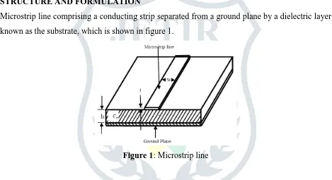
Microstrip line comprising a conducting strip separated from a ground plane by a dielectric layer
known as the substrate, which is shown in figure 1.
Figure 1: Microstrip line
In microstrip, the stripline and ground plane are located on opposite sides of the substrate.
Because of the coupling of electromagnetic fields, a pair of coupled lines can support two
different modes of propagation known as odd and even modes. These modes have different
characteristics impedances. The velocity of propagation of these two modes is equal, when the lines are imbedded within an infinite homogeneous dielectric medium. But for coupled
microstrip lines involving in homogeneous medium, a part of the field extends into the air above the substrate. This fraction is different for the two modes of coupled lines. Consequently, the
effective dielectric constants are not equal for the two modes. When the two conductors of a
coupled line pair are identical we have a symmetrical configuration. This symmetry is very
useful for simplifying the analysis and design of such coupled lines. If the two lines do not have
reader with a comprehensive analysis of all fundamental concepts related to the open
symmetrical coupled microstrip transmission lines.
ANALYSIS BY QUASI STATIC
A Microstrip line can be quasi-statically analyzed by the use of elliptical integral formulae. It
consists in transforming the geometry of the PCB into another conformation.
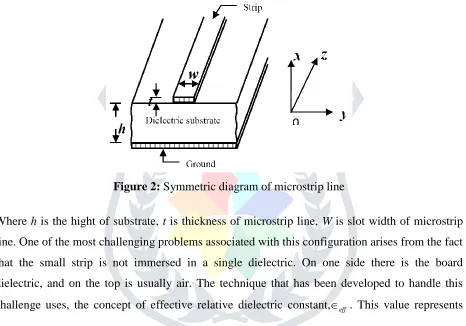
Figure 2: Symmetric diagram of microstrip line
Where h is the hight of substrate, t is thickness of microstrip line, W is slot width of microstrip line. One of the most challenging problems associated with this configuration arises from the fact
that the small strip is not immersed in a single dielectric. On one side there is the board
dielectric, and on the top is usually air. The technique that has been developed to handle this
challenge uses, the concept of effective relative dielectric constant,eff . This value represents
some intermediate value between the relative dielectric constant of the board material, r, and that of air (assumed equal to 1) that can be used to compute microstrip parameters as though the
strip were completely surrounded by material of that effective relative dielectric constant. One
obvious advantage of the microstrip structure is the "open" line which makes it very easy to
connect components. Aside from the difficulty of calculating the value of eff , there is another
important effect. It is clear that eff will depend on both W and h. Hence, the phase velocity along
the microstrip will depend on these parameters. Assuming the relative permeability of all
materials in the line design is well approximated by r 1, the phase velocity will be given by
p
eff
c
Since the characteristic impedance 𝑍𝑜 of the line will also depend on these parameters, every
time we need to design a microstrip with a new characteristic impedance, we will be faced with
the additional complication of having to deal with a change in phase velocity (or delay time) and
consequently of the wavelength of waves on that microstrip. To get an idea of the range of εeff,
consider the cases of a very wide width W and then a very narrow width W.
𝑚𝑎𝑥𝑖𝑚𝑢𝑚 eff r ...(2)
Eqn. (2) is in the form of an "effective" microstrip width (We), which is used to replace W.
For a wide microstrip, nearly all of the electric field lines will be concentrated between
the metal planes, similar to the case of a parallel plate capacitor, and for narrow width W the
electric field lines will be about equally divided between the air and the board dielectric so that:
𝑚𝑎𝑥𝑖𝑚𝑢𝑚 1
1
2eff r
...(3)
This gives a range:
1 1
2 r eff r ...(4) Several different equations have been developed for use in calculating characteristic impedance
for microstrip design. Probably the most useful are the following which are reported to be
accurate to within about 1%.
0 60 ln 8 4 eff h W Z W h
...(5)
Where
1
2 2
1 1
1 12 0.04 1 1
2 2
r r
eff
h W W
for
W h h
...(6) 0 120
1.393 0.667 ln 1.444
eff Z W W h h ...(7) Where 1 2 1 1
1 12 1
2 2 r r eff h W for W h ...(8)
These are relatively equations for the calculation of characteristic impedance, given W, h, and
eff
required characteristic impedance. Here, then, is the design challenge since the equations are
transcendental for the W
h parameter. Now, modify to the above equations which is a consequence of considering the finite thickness (t) of the microstrip. This modification is in the form of an "effective" Microstrip width (We), which is used to replace W in those equations:
2 1
1 ln
2 e
t h W
W W for
t h
...(9)
4 1
1 ln
2 e
t W W
W W for
t h
...(10)
RESULT AND DISCUSSION
a.) CHARACTERISTIC IMPEDANCE V/S NORMALISED STRIP WIDTH
Normalized strip width is known as ratio of width of Microstrip line and height of the
substrate. The graph represents the variation of characteristic impedance with normalized strip
width for substrate is chosen to be of glass fiber.
1.1 Normalized strip width when 𝒘/𝒉 ≤ 𝟏
Graph 1.1 shows the variation of characteristic impedance with normalized strip width.
Graph1.1. variation of characteristic impedance v/snormalized strip width
1.2 Normalized strip width when 𝒘/𝒉 ≥ 𝟏
Graph1.2. variation of characteristic impedance v/s normalized strip width
As seen in both the above graph, that when normalized strip width is kept between 1 to 5, then
the characteristic impedance decreases with increases in normalized strip width. But when the
same normalized strip width is kept between 0 to 1 then there is a sudden and rapid decrease in
characteristic impedance
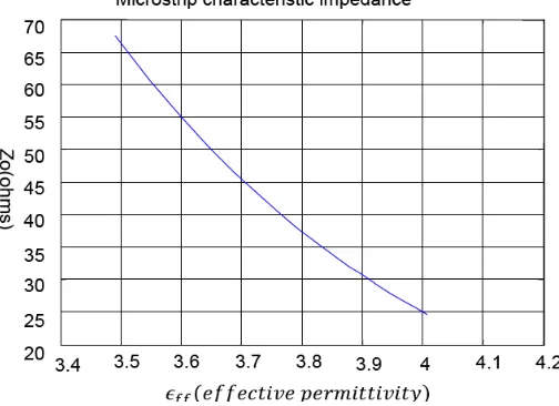
b) CHARACTERISTIC IMPEDANCE V/S EFFECTIVE PERMITIVITY 2.1 Effective permittivity for 𝒘/𝒉 ≥ 𝟏
Graph 2.1 shows the variation of characteristic impedance with different value of
effective permittivity. In this graph it is clear that, as we increase the effective relative
permittivity, the value of characteristic impedance decreases when the value of normalized strip
Graph2.1: variation of characteristic impedance v/s effective permittivity
2.2 Effective permittivity for 𝒘/𝒉 ≤ 𝟏
Figure 4.4 shows the variation of characteristic impedance with different value of
effective permittivity. In the graph it is clear that, as we increase the effective relative
permittivity, the value of characteristic impedance decreases when the value of normalized strip
width is less than equal to 1.
Graph2.2: variation of characteristic impedance v/s effective permittivity
The characteristic impedance of any type of transmission line decreases with increase in relative
0
R j L
Z
G j C
...(11)
Where,
R = Resistance per unit length, L = Inductance per unit length G = Conductance per unit length C = Capacitance per unit length
Form the above mention formula, the condition arises R × C = L × G for distortion less transmission line. Since there is no wires or long conducting element L and G cannot be changed so it is very evident from the above condition that only R and C can be inversely proportional to each other as C is dependent on relative permittivity and R can be treated as characteristic
impedance it can be knuckled with the fact that whenever C Increases R decreases.
CONCLUSION
Work has been done to demonstrate the utility of microstrip line and its advantages
especially energy is to be transferred from one point to another, in a very compact and efficient
form. A simple and inexpensive method also known as quasi-static has been applied for
calculating the characteristic impedance as well as effective permittivity. Variation of
characteristic impedance for different value of normalized strip width as well as different value
of effective permittivity is represented. It has been observed that characteristic impedance
decreases with advancement of normalized strip width and also decreases for increasing effective
permittivity. This property can be applied in microwave transmission theory to design different
antenna models for different purposes along with the advantage of minimal distortion, and
avoiding high cross-talk and radiation.
REFRENCES
[1] Baklem and A. Dmar, “Invarted Defected Ground Structure for Microstrip line filter
reducing Packaging Complicity, Department of Electrical, Czech Technical University,
2008.
[2] A. Z. Elsherbeni, C. E. Smith and B. Moumnch, “Minimization of the Coupling between
a two Conductor Mirostrip Transmission Line using Finite difference Method”, Journal
[3] B. Easter, “The Equivalent Circuit of some Microstrip Discontinuities”, IEEE Transaction on Microwave Theory and Techniques, Vol. 23, No. 8, PP.655-660 Aug. 1975.
[4] C. K. Wu and H. S. Wu, “Electric- Magnetic- Electric Slow-Wave Microstrip Line and
Bond pass Filter of Compressed Size”, IEEE Transaction on Microwave Theory and
Techniques, Vol. 50, No. 8, Aug, 2002.
[5] E. Tunier. Lee B. T., M. Islam and D. P. Nickirk, “Quasi-Static Conductor Loss
Calculations in Transmission Theory and Techniques, Vol. 42, PP. 1807-1815, 1994.
[6] E. Tunnier, and P. Nickirk, “Highly Accurate Quasi-Static Modding of Microstrip Lines
over Lossy Subptrates”, IEEE Microwave and Guided Wave Letter, Vol. 2, No. 10,
October 1992.
[7] E. Yamshita, “Variational Method for the Analysis of Microstrip Like Transmission
Lines”, IEEE Transaction on Microwave Theory and Techniques, Vol. 16 No. 8, Aug,
1968.
[8] H. Wang, Y. Ji, and T. H. Hubiay, “Experimental and Numerical study of the Radiation
from Microstrip Bends”, University of Missouri-Rolla, 2000.
[9] J. C. Rautis, and V. Demir, “Microstrip Conductor loss Models for Electro-Magnetic
Analysis”, IEEE Transaction on Microwave Theory and Techniques, Vol. 51, No. 3,
March. 2003.
[10] J. S. Lim, C.S. Kim and J. S. Park, “Design of 10.1B 900 Branch Line Coupler using
Microstrip Line with defected ground Structure”, Electronics Letters, Vol. 56, No. 21,
Oct. 2000.
[11] M. E. Goldforb and R. A. Pucel, “Modding Via Hole Grounds in Microstrip,” IEEE
Microwave and Guided Ware Letters, Vol.1, No. 6, PP. 135-137, June 1991.
[12] M. Kahrizi, K. Sarkar and Zoran A. Maricevic, “Dynamic Analysis of a Microstrip Line
Over a Perforated Ground Plane”, IEEE Transaction on Microwave Theory and
Techniques, Vol. 42, No. 5, May 1994.
[13] N. Jain and B. Brown, “Dispersion Characteristics of Microstrip Transmission line on
Glass Microwave IC’S”, IEEE Microwave and Guided Wave Letter, Vol. 7, No. 10, Oct.
1997.
[14] R.J. Akello, B. Easter, and I.M. Stephenson, “Equivalent circuit of the symmetric