Low Power SRAM with Boost Driver Generating
Pulsed Word Line Voltage for Sub-1V Operation
Masaaki Iijima, Kayoko Seto, Masahiro Numa† Kobe University 1-1 Rokko-dai, Nada, Kobe 657-8501 Japan
†Email: [email protected]
Akira Tada, Takashi Ipposhi††
Renesas Technology Corp. 4-1 Mizuhara, Itami, Hyogo 664-0005 Japan ††Email: [email protected]
Abstract—Instability of SRAM memory cells derived from the process variation and lowered supply voltage has recently been posing significant design challenges for low power SoCs. This paper presents a boosted word line voltage scheme, where an active body-biasing controlled boost transistor generates a pulsed word line voltage by capacitive coupling only when accessed. Simulation results have shown that the proposed approach not only shortens the access time but mitigates the impact of Vth variation on
performance even at ultra low supply voltage less than 0.5 V.
Index Terms— SRAM, Circuit methodology, Low power, Low voltage, PD-SOI, Vth variation
I. INTRODUCTION
In recent years, lots of serious problems in accordance with aggressive technology scaling, known as “red brick wall,” have been posing significant design challenges for performance improvement of LSI’s. Power reduction is becoming one of the most critical design issues especially for battery-operated portable devices due to severe power constraints. In addition, since the area of on-chip SRAM memory has been continuing to grow, both the active and leakage power consumption on memory area dominates the total chip power [1]. Hence, power management in SRAM operating at low power consumption is in-dispensable for future system LSI designs. Therefore, we propose a circuit design methodology for low power SRAM with single supply voltage. The rest of this paper is organized as follows. First, Section II gives an overview of previous low power approaches mainly focusing on dynamic voltage control with multiple supply voltages. Next, Section III refers several issues of SRAM operating at low supply voltage. Then, we propose a boosted word line voltage scheme for single power supply SRAM employing capacitive coupling of ABC (Active Body-biasing Controlled)-SOI capacitor in Section IV. Section V provides circuit simulation results. Finally, we summarize the key results in Section VI.
II. LOW POWER TECHNIQUE BY DYNAMIC VOLTAGE CONTROL
Lowering the supply voltage (VDD) has been one of the most effective approaches in order to pursue ultra low power operation since the dynamic power consumption decreases in proportion to the square of VDD. The lowered supply voltage also has an advantage of reduction in the leakage power consumption derived from the sub-threshold and gate leakage current during the standby mode. A VDD-hopping scheme [2] where the supply voltage is dynamically controlled according to workload of a processor is known as one of the representative low power design methodologies employing hardware-software cooperatively oriented algorithm. In addition, a DVS (Dynamic Voltage Scaling) [3] and a DVFS (Dynamic Voltage Frequency Scaling) [4], lowering a frequency and supply voltage as long as lower performance is allowed, are becoming a standard approach for reducing active power consumption when performance requirements vary. The design style of voltage scaling which is moving from coarse-grained approaches to fine-grained ones even aims at scaling the threshold voltage (Vth) in small steps [5].
III. ISSUES OF SRAMOPERATING AT LOW SUPPLY VOLTAGE
time in low voltage operation. The use of 8T-SRAM [9] with a separated read-port has been discussed to enhance the stability by eliminating cell disturbs during a read access even when VDD is scaled down to sub-1V. However, additional transistors unfortunately deteriorate the write access time for 8T-SRAM as lowered supply voltage. Hence, it is important to accelerate the write/read access time even in low voltage operation while maintaining the SNM.
In this paper, we propose a design methodology employing a boosted voltage scheme with a single power supply rail which can be widely applied and especially aims at 8T-SRAM for the SNM improvement. In the case of 6-transistor SRAM basic memory cells shown in Fig. 1, the access time for read and write operation mainly depends on the access transistors connecting bit lines (BL, BLB) and a cross-coupled inverter latch. Here, the access transistors consist of nMOS pass-transistors with the disadvantage of the output voltage drop at high level. Even though the drain voltage Vdrn is expected to be Vdrn = VDD, the drain voltage actually rises only up to Vdrn = (VDD – Vth), which results in a lack of on-current. The issue of voltage loss is becoming more serious in accordance with lowered supply voltage since Vth is scaled down more moderately than VDD. To avoid them, we propose a speed-up technique boosting the word line node for reduction in voltage loss based on a bootstrap scheme [10] employing an ABC-SOI for strong capacitive coupling. Our strategy includes the following two features:
i) Boosting the word line nodes quickly by a Bootstrap-type driver.
ii) Strong boosting effect by the Active Body-biasing Control.
IV. BOOSTED WORD LINE VOLTAGE SCHEME FOR SINGLE POWER SUPPLY SRAM
In this section, we propose a novel design style for SRAM employing the ABC-Bootstrap scheme which boosts the word line node voltage higher than VDD to accelerate the write / read speed. In SRAM memory cells, two bit lines and a cross-coupled inverter latch are connected each other through access transistors while the word line activates the access transistors. Then, the write / read operation can be performed by draining on-current at the access transistors. Thus, enhancing the current from bit lines to memory cells helps shorten the delay time in the write mode. On the other hand, in the read operation mode, two bit lines BL and BLB are first charged to VDD during the precharge operation. Then, the carrier at BL or BLB are discharged to the data retention node of “Low” in memory cells right after turning on the access transistors. A sense amplifier detects the difference of bit line voltages between BL and BLB and outputs the data stored in memory cells. Hence, lowering the bit line voltage in short transition time by enhancing the on-current of access transistors is effective for fast read operation. Therefore, boosting the gate voltage of access transistors is expected to shorten both the write and read access time.
A. ABC-SOI Capacitor
The Active Body-biasing Controlled (ABC)-SOI capacitor utilizing the PD-SOI process with the Hybrid Trench Isolation technology [11], [12] provides a strong capacitive coupling.
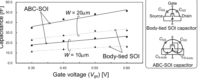
The strength of capacitive coupling is dependent upon a transistor size and gate voltage. For an nMOS FET with the gate length L = 0.18 µm and the gate width W = 10, 20 µm, we have calculated the capacitance between the gate and source/drain when the gate voltage changes from 0.3 V to 0.6 V. According to the SPICE simulation results shown in Fig. 2, the capacitance is proportional to the gate voltage since the capacitances in the channel of transistor increases in accordance with the gate voltage while the overlap capacitance becomes a constant value.
BL WL
BLB
Access transistor
Driver transistor
Load transistor
Access transistor
Figure 1. 6T-SRAM memory cell.
0.0 10.0 20.0 30.0 40.0 50.0 60.0
0.25 0.30 0.35 0.40 0.45 0.50 0.55 0.60 0.65
ABC-SOI
Body-tied SOI W= 10µm
W= 20µm
Gate voltage(Vgs) [V]
Cap
ac
itance [fF
]
Body-tied SOI capacitor
ABC-SOI capacitor
CGS
Drain Source
CGD Gate
CS-body CD-body CGS CGD
In addition, even though the capacitance in body-tied SOI mainly derives from the overlap capacitances between the gate and source/drain (CGS, CGD), the ABC-SOI capacitor, where the body is directly connected to the gate, provides the enhanced capacitance owing to the additional capacitances (CS-body, CD-body) between the source/drain and body. We take the advantage of strong capacitive coupling by the ABC-SOI.
B. Word Line Driver with ABC-SOI Capacitor
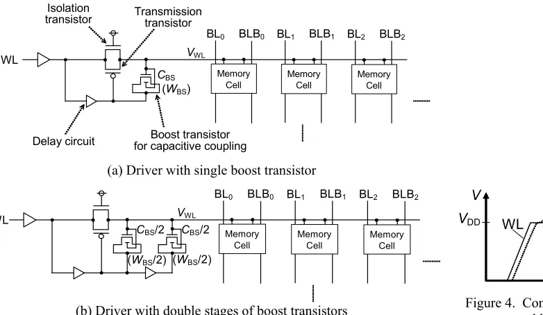
The proposed approach, boosted voltage scheme with the ABC-SOI capacitor, is shown in Fig. 3. We describe the features in detail.
First, during a low to high transition of the word line as shown in Fig. 4, the pMOS in the transmission gate helps finish the pull-up transition perfectly since the pMOS keeps on-state until the input signal WL via delay circuits cuts off the pMOS. Thus, the word line voltage VWL is allowed to rise up to VDD immediately. Second, the capacitance CBS of the boost transistor starts to boost VWL higher than VDD as illustrated in Fig. 4 as soon as the pMOS turns off in the driver circuit with the single boost transistor shown in Fig. 3 (a). In addition, the driver with double stages of the boost transistor, shown in Fig. 3 (b), divides the capacitance CBS into two boost transistors. The second stage of the boost transistor driven by the second delay circuit prevents VWL from dropping when VWL is boosted by the first stage of the boost transistor. In Fig. 3 (a), VWL actually drops a little due to the current passing through the pMOS before turning off perfectly. Hence, employing double stages of the boost transistor enhances the capacitive coupling and ensures boosting VWL higher than VDD. The higher gate voltage results in an enhanced on-current of the access transistors.
C. Boosting Effect of Word Line Voltage
Here, we discuss the boosting effect of the word line voltage. In fact, the capacitive coupling by the boost
transistors dominates the maximum voltage level of word line, which boosts the word line voltage VWL up to
DD total
BS
WL 1 C V
C
V ⎟⎟
⎠ ⎞ ⎜⎜
⎝ ⎛
+ =
, (1)
where CBS denotes the capacitance between the gate and source / drain of boost transistors, and Ctotal denotes the total capacitance including the wire capacitance of word line CWL. Thus, the strength of capacitive coupling depends upon the ratio of CBS to Ctotal. Here, CBS is proportional to the gate width WBS of the boost transistor as already shown in Fig. 2, and CWL is in proportion to the length of word line, thus, the number of memory cells in each row. Then, Fig. 5 shows the ratio of word line voltage VWL to VDD (VWL / VDD) calculated by Equation (1) when the number of memory cells arrayed in each row varies. For simplicity, we treat Ctotal as Ctotal = CBS + CWL. The capacitance of boost transistors for capacitive coupling has been set to CBS = 14 fF,28 fF when the gate width WBS = 10 µm,20 µm, respectively. We have assumed that the wire capacitance of word line per memory cell is CWL = 1.25 fF/cell. In Fig. 5, in the case memory cells of 32-bit are arrayed in each row, for example, the ratio VWL / VDD = 1.4 when the gate width WBS = 20 µm, while the maximum voltage level of word line results in tendency to decrease as the number of bit increases. Hence, an adequate ratio of VWL / VDD ensures low voltage operation and shortens the access time.
V. SIMULATION RESULTS
We have performed SPICE simulation with the BSIM3-based SOI transistor model for 0.18 µm PD-SOI process in order to evaluate our Enhanced ABC-Bootstrap scheme. The threshold voltages with MOSFETs are set to Vth-n = 0.34 V, Vth-p = −0.42 V for memory cells and Vth-n = 0.24 V, Vth-p = − 0.34 V for address decoders or
WL
V
t VDD
VWL
Figure 4. Concept of boosted word line voltage.
Isolation transistor
WL
Memory Cell
Memory Cell
Memory Cell
Transmission transistor
Boost transistor for capacitive coupling
VWL
BL0 BLB0 BL1 BLB1 BL2 BLB2
Delay circuit
CBS
(WBS)
(a) Driver with single boost transistor
WL
Memory Cell
Memory Cell
Memory Cell
VWL
BL0 BLB0 BL1 BLB1 BL2 BLB2
CBS/2 CBS/2
(WBS/2)
(WBS/2)
(b) Driver with double stages of boost transistors
peripheral circuits. We define these threshold voltages Vth-n, Vth-p as the gate voltage which makes the drain current Ids per width W to be 1 µA/µm when the drain voltage Vds = 1.8 V. We have calculated them by SPICE simulation. We extracted the resistance and capacitance of the wire after designing the 8Kb memory array. We have decided that the gate width W = 5 µm for the word line driver, isolation transistor, and transmission transistor and W = 10 µm for the boost transistor, respectively. With respect to the whole layout area of 8 Kb memory array, for example, our boosted voltage scheme has an area overhead of 10 % due to the additional area of word line drivers.
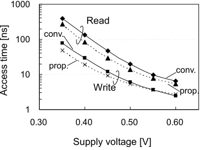
We have evaluated the access time to a memory cell in the write and read operation mode for the supply voltages from 0.35 V to 0.6 V. A variation in the threshold voltage is also discussed. The Enhanced ABC-Bootstrap scheme has been compared to the SRAM configuration with the normal word line driver without the Bootstrap scheme. A. Write Operation Speed
First, we discuss the write operation speed to memory cells based on the results shown in Fig. 6. We also consider the waveforms of the clock CK, word line WL, and data-retention node in Fig. 7 (a). Here, we define the
write time as the period from the point of VDD / 2 in CK during a low to high transition to that in the date retention node of memory cells during the data inverting operation. We have achieved 10%, 38 % of improvements in the write time at VDD = 0.5 V, VDD = 0.35 V, respectively. This results show our approach is more effective to the lower supply voltage. The data retention node of memory cell in our approach completes charging quickly owing to the boosted word line voltage as shown in Fig. 7 (a). Here, the ratio of word line voltage VWL to VDD in Fig. 7 becomes VWL / VDD = 1.25 that approximates the value calculated by Equation (1) as shown in Fig. 5 even though VWL is lowered a little due to discharging through the transmission transistor.
According to Fig. 6, the write time increases exponentially since lowering supply voltage degrades driving power of transistors in the both approaches. Then, we have confirmed that the proposed approach requires the longer write time than the conventional one if the supply voltage is over 0.5 V. On the other hand, the relation became inverted when it comes to ultra low supply voltage less than 0.5 V. We consider the results from the point of the dependence on the delay time of tWL
0.0 0.5 1.0 1.5 2.0
10 100 1,000
WBS = 10 µm
VWL
/
VDD
WBS = 20 µm
10 20 50 100 200 500 1000 Bit (# of memory cells in each row)
Figure 5. Ratio of boosted word line voltage to power supply (VWL / VDD) depending on the number of bit cells.
CK
Data node(prop.) Data node(normal) 19.3 ns
29.1 ns WL(prop.) WL(normal)
WL(prop.)
BL(prop.) BL(normal)
BLout(prop.)
BLout(normal)
131 ns 82.5 ns
WL(normal)
CK
(a) Write mode (b) Read mode
Figure 7. Waveforms.
1 10 100 1000
0.30 0.40 0.50 0.60
prop. conv.
Supply voltage [V]
Ac
ce
ss
tim
e
[n
s] Read
Write
prop. conv.
and taccess, where tWL represents the propagation delay of the word line and taccess means the gate delay of the access transistor. At the higher voltage operation, both tWL and taccess have almost the same order of delay time owing to enough driving power. Hence, the proposed approach shows the longer write time since the additional input load to the word line causes the extra delay of tWL. On the other hand, taccess becomes much longer than tWL due to the higher threshold voltage of the access transistors as the supply voltage goes down, which conceals the extra delay of tWL. Thus, the gate voltage higher than VDD shortens the write time in the proposed approach at low supply voltage less than 0.5 V.
B. Read Operation Speed
Next, we show the simulation results with the read time in Fig. 6. We also consider the waveforms of the clock CK, word line WL, bit line BL, and output data signal from sense amplifier BLout as illustrated in Fig. 7 (b). Here, we define the read time as the period from the point of VDD / 2 in CK during a low to high transition to that in BLout, while the sense amplifier detects the difference of bit line voltages between BL and BLB and outputs the data stored in memory cells. According to Fig. 8, the lower supply voltage increases the read time exponentially. Our proposed approach shortens the read time by 15 % at VDD = 0.5 V and 30 % at VDD = 0.35 V compared to the conventional approach. Since the read time is dependent on the discharging speed of bit line, enhancing the on-current of access transistors by boosted the word line voltage higher than VDD achieves quick discharging operation of bit line as shown in Fig. 7 (b). As a result, the bit line voltage in the proposed approach drops in shorter transition time than the conventional one. Therefore, the output data in the proposed approach appears first by the quick response of sense amplifier. C. Vth Dependance of Access Time
Here, we analyze the dependence of access time derived from a variation in the threshold voltage (Vth). In the low voltage operation such as 0.5 V-VDD, transistors come into the linear or sub-threshold operation since the supply voltage almost reaches the threshold voltage. Especially
for SRAM memory cells, their performance is directly dependent upon the on current of access transistors which varies due to Vth variation. Then, we have evaluated the difference in access time derived from Vth variation between the conventional approach and proposed one through HSPICE simulation.
First, best and worst cases have been analyzed. We have decided that the mean of the threshold voltage Vth0 = 346 mV and assume a variation of ± 10% as the best and worst cases. Fig. 8 shows the access time of memory cell when Vth0 changes from 0.9Vth0 to 1.1Vth0. With respect to the difference in access time between the fastest and slowest cases, the maximum difference results in 2.54x in the read mode for the conventional approach. On the other hand, the difference is suppressed down to 1.99x in our approach since the enhanced on current of access transistors by the boosted gate voltage avoids a larger impact of Vth variation. The difference in write time is likewise reduced from 1.53x to 1.21x. Therefore, a smaller variation in the access time due to Vth variation is expected in our approach.
Next, the impact of Vth variation on the distribution of write time has also been analyzed based on the 1k-point Monte Carlo simulations. Here, the global and local Vth variations of 3σ are reflected to the histograms shown in Fig. 9, where the standard deviation σ of Vth is assumed
1.0 10.0 100.0
300 350 400
A
cc
ess t
im
e
[n
s]
Threshold voltage (Vth) [mV]
Read
Write
conv.
prop.
conv. prop. 1.99x 2.54x
1.53x
1.21x
mV 346 V,
5 .
0 th0
DD= V =
V
)
(Vth0 (Vth0+3.3%) (Vth0+10%) %)
3 . 3 (Vth0− %) 10 (Vth0−
Figure 8. Vth dependence of access time based on best and worst analyses.
0.0 5.0 10.0 15.0
0.0 20.0 40.0
0.80x
0.74x
0.70x
Power consu
m
pt
ion
[n
W
]
Access time [ns] conv. prop.
Figure 10. Power saving effect. 0
100 200 300 400 500
4.00 5.00 6.00 7.00
Access time (write) [ns]
O
cc
urrenc
es
conv. prop.
µ = 5.78 ns
σ = 0.37 ns
σ/µ: 6.4%
µ= 5.39 ns
σ = 0.23 ns
σ/µ: 4.3%
that 3 σ corresponds to 10 % of Vth. According to the mean (µ) and standard deviation (σ) of access time summarized in Fig. 9, the proposed approach reduces the
µ and σ by 7 % and 38 %, respectively. As a result, the coefficient of variation (CV: σ/µ) is improved from 6.4 % to 4.3 %.
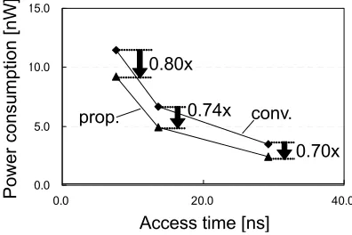
D. Power Saving Effect
Using the lower supply voltage is allowed in our approach while maintaining the same operational speed as the conventional approach. Here, we discuss the power saving effect based on Fig. 10. We compare the power consumption in both approaches after adjusting the proper supply voltage in order to achieve the same operational speed. According to Fig. 10, the Enhanced ABC-Bootstrap scheme achieves the power reduction of 30 % in the best case in spite of the additional word line driver in the proposed scheme. It means that the power consumed by a charging and discharging the bit lines dominates the whole power of SRAM, the additional power in the proposed word line driver can be less significant. Therefore, our SOI-SRAM with the Enhanced ABC-Bootstrap scheme ensures LSIs’ operation even at ultra low supply voltage.
VI. CONCLUSION
In this paper, in order for SRAM to pursue low voltage operation, we have proposed a low power design methodology employing a boost driver which generates a pulsed word line voltage for single power supply and sub-1V operation. In the proposed word line driver circuit, the use of an active body-biasing controlled boost transistor enhances the impact of capacitive coupling, and the boosted the word line voltage increases the on-current of access transistor. Simulation results have shown the proposed approach not only shortens the access time but mitigates the impact of global and local Vth variation on performance even at ultra low supply voltage less than 0.5V.
REFERENCES
[1] International Technology Roadmap for Semiconductor
2005.
[2] H. Kawaguchi, G. Zhang, S. Lee, Y. Shin, and T. Sakurai,
“A controller LSI for realizing VDD-hopping scheme with
off-the-shelf processors and its application to MPEG4,”
IEICE Trans. on Electronics, vol. E85-C, no. 2, pp. 263-271, Feb. 2002.
[3] B. H. Calhoun and A. Chandrakasan, Ultra-dynamic
voltage scaling using sub-threshold operation and local
voltage dithering in 90nm CMOS, in IEEE ISSCC Dig.
Tech. Papers, pp. 300-301, Feb. 2005.
[4] T. Fujiyoshi, S. Shiratake, S. Nomura, T. Nishikawa, Y.
Kitasho, H. Arakida, Y. Okuda, Y. Tsuboi, M. Hamada, H. Hara, T. Fujita, F. Hatori, T. Shimazawa, K. Yahagi, H. Takeda, M. Murakata, F. Minami, N. Kawabe, T. Kitahara, K. Seta, M. Takahashi, Y. Oowaki, and T. Furuyama, “An H.264/MPEG-4 Audio/Visual Codec LSI with Modulewise
Dynamic Voltage/Frequency Scaling,” in IEEE ISSCC Dig.
Tech. Papers, pp. 132-133, Feb. 2005.
[5] M. Nomura, Y. Ikenaga, K. Takeda, Y. Nakazawa, Y.
Aimoto, and Y. Hagihara, “Monitoring Scheme for Minimizing Power Consumption by Means of Supply and Threshold Voltage Control in Active and Standby Modes,” in Symp. VLSI Circuits Dig. Tech. Papers, pp. 308-311, June 2005.
[6] E. Seevinck, F. J. List, and J. Lohstroh, “Static-Noise
Margin Analysis of MOS SRAM Cells,” IEEE J.
Solid-State Circuits, vol. sc-22, pp. 748-754, Oct. 1987.
[7] K. Itoh, A. R. Fridi, A. Bellaou, and M. I. Elmasry, “A
deep sub-V, single power-supply SRAM cell with
multi-VT, boosted storage node and dynamic load,” in Symp.
VLSI Circuits Dig. of Tech. Papers, pp. 132-133, June 1996.
[8] M. Yamaoka, K. Osada, and K. Ishibashi, “0.4-V Logic
Library Friendly SRAM Array Using
Rectangular-Diffusion Cell and Delta-Array-Voltage Scheme,” in Symp.
VLSI Circuits Dig. Tech. Papers, pp. 170-173, June 2002.
[9] L. Chang, D. M. Fried, J. Hergenrother, J. W. Sleight, R. H.
Dennard, R. K. Montoye, L. Sekaric, S. J. McNab, A. W. Topol, C. D. Adams, K. W. Geuarini, and W. Haensch, “Stable SRAM Cell Design for the 32nm Node and
Beyond,” in Symp. VLSI Technology Dig. Tech. Papers, pp.
128-129, June 2005.
[10]M. Iijima, M. Kitamura, K. Hamada, K. Fukuoka, M.
Numa, A. Tada, and S. Maegawa, “Active Body-Biasing Control Technique for Bootstrap Pass-Transistor Logic on
PD-SOI at 0.5V-VDD,” in Proc. IEEE International SOI
Conference, pp. 50-51, Oct. 2005.
[11]Y. Hirano, T. Matsumoto, S. Maeda, T. Iwamatsu, T.
Kunikiyo, K. Nii, K. Yamamoto, Y. Yamaguchi, T.
Ipposhi, S. Maegawa, and M. Inuishi, “Impact of 0.10 µm
SOI CMOS with Body-Tied Hybrid Trench Isolation Structure to Break Through the Scaling Crisis of Silicon
Technology,” in IEDM Tech. Dig., pp. 467-470, Dec. 2000.
[12]Y. Hirano, T. Ipposhi, H. Dang, T. Matsumoto, T.
Iwamatsu, K. Nii, Y. Tsukamoto, H. Kato, S. Maegawa, K. Arimoto, Y. Inoue, M. Inuishi, and Y. Ohji, “Impact of Actively Body-bias Controlled (ABC) SOI SRAM by using Direct Body Contact Technology for Low-Voltage
Application,” in IEDM Tech. Dig., pp. 2.4.1-2.4.4, Dec.
2003.
Masaaki Iijima received the B.E., and M.E. degrees in Electrical and Electronics Engineering from Kobe University, Kobe Japan, in 2003, and 2005, respectively. Since 2005, he has been in Graduate School of Science and Technology, Kobe University, and is currently a doctoral candidate. His research interest includes low power circuits design especially for SOI devices. He is a member of the IEEE, IEICE, and IPSJ.
Kayoko Seto received the B.E. degrees in Electrical and Electronics Engineering from Kobe University, Kobe Japan, in 2007. Since 2007, she has been in Graduate School of Engineering, Kobe University, and is currently a master candidate. Her research interest includes low power and high reliability SRAM circuit design. She is a member of the IEICE.
and image processing. He is a member of the IEEE, ACM, IEICE, and IPSJ.
Akira Tada received the B.E. and M.E. degrees in electrical and electronics engineering from Kobe University, Hyogo, Japan, in 1995 and 1997, respectively. In 1997 he joined Mitsubishi Electric Corporation, Hyogo, Japan. Since then, he has been engaged in the development of CAD for LSI design. Since 2003, he has been with Renesas Technology Corporation, Hyogo, Japan. He is a member of the IEEE, IEICE and IPSJ.