University of Windsor University of Windsor
Scholarship at UWindsor
Scholarship at UWindsor
Electronic Theses and Dissertations Theses, Dissertations, and Major Papers
10-5-2017
Experimental Evaluation and Comparison of Time-Multiplexed
Experimental Evaluation and Comparison of Time-Multiplexed
Multi-FPGA Routing Architectures
Multi-FPGA Routing Architectures
Asmeen Kashif
University of Windsor
Follow this and additional works at: https://scholar.uwindsor.ca/etd
Recommended Citation Recommended Citation
Kashif, Asmeen, "Experimental Evaluation and Comparison of Time-Multiplexed Multi-FPGA Routing Architectures" (2017). Electronic Theses and Dissertations. 7269.
https://scholar.uwindsor.ca/etd/7269
This online database contains the full-text of PhD dissertations and Masters’ theses of University of Windsor students from 1954 forward. These documents are made available for personal study and research purposes only, in accordance with the Canadian Copyright Act and the Creative Commons license—CC BY-NC-ND (Attribution, Non-Commercial, No Derivative Works). Under this license, works must always be attributed to the copyright holder (original author), cannot be used for any commercial purposes, and may not be altered. Any other use would require the permission of the copyright holder. Students may inquire about withdrawing their dissertation and/or thesis from this database. For additional inquiries, please contact the repository administrator via email
Experimental Evaluation and Comparison of Time-Multiplexed Multi-FPGA Routing Architectures
By
Asmeen Kashif
A Dissertation
Submitted to the Faculty of Graduate Studies
through the Department of Electrical and Computer Engineering in Partial Fulfillment of the Requirements for
the Degree of Doctor of Philosophy at the University of Windsor
Windsor, Ontario, Canada
2017
Experimental Evaluation and Comparison of Time-Multiplexed Multi-FPGA Routing Architectures
by
Asmeen Kashif
APPROVED BY:
__________________________________________________ F. Gebali, External Examiner
Department of Electrical & Computer Engineering University of Victoria
__________________________________________________ W. Abdul-Kader
Department of Mechanical, Automotive & Materials Engineering
__________________________________________________ J. Wu
Department of Electrical & Computer Engineering
__________________________________________________ H. Wu
Department of Electrical & Computer Engineering
__________________________________________________ M. Khalid, Advisor
Department of Electrical & Computer Engineering
iii
DECLARATION OF PREVIOUS PUBLICATIONS
This thesis includes 3 original papers that have been previously submitted for
publication in peer reviewed journals, as follows:
Thesis
Chapter
Publication title/full citation Publication status*
Chapter [3]
[6] [7]
Experimental Evaluation and
Comparison of Time-Multiplexed
Schemes and Routing Architectures for
Multi-FPGA Systems
submitted
Chapter [4]
[5] [7]
Latency-Optimized 3D Multi-FPGA
System with Serial Optical Interface
submitted
Chapter [4]
[6] [7]
Experimental Evaluation and
Comparison of Latency-Optimized
Optical and Conventional Multi-FPGA
Systems
submitted
I certify that I have obtained a written permission from the copyright owner(s) to
include the above published material(s) in my thesis. I certify that the above material
describes work completed during my registration as a graduate student at the University of
Windsor.
I certify that, to the best of my knowledge, my thesis does not infringe upon
anyone’s copyright nor violate any proprietary rights and that any ideas, techniques,
quotations, or any other material from the work of other people included in my thesis,
published or otherwise, are fully acknowledged in accordance with the standard
referencing practices. Furthermore, to the extent that I have included copyrighted material
that surpasses the bounds of fair dealing within the meaning of the Canada Copyright Act,
iv
such material(s) in my thesis and have included copies of such copyright clearances to my
appendix.
I declare that this is a true copy of my thesis, including any final revisions, as
approved by my thesis committee and the Graduate Studies office, and that this thesis has
v
ABSTRACT
Emulating large complex designs require multi-FPGA systems (MFS). However,
inter-FPGA communication is confronted by the challenge of lack of interconnect capacity due
to limited number of FPGA input/output (I/O) pins. Serializing parallel signals onto a
single trace effectively addresses the limited I/O pin obstacle. Besides the multiplexing
scheme and multiplexing ratio (number of inter-FPGA signals per trace), the choice of the
MFS routing architecture also affect the critical path latency. The routing architecture of
an MFS is the interconnection pattern of FPGAs, fixed wires and/or programmable
interconnect chips. Performance of existing MFS routing architectures is also limited by
off-chip interface selection.
In this dissertation we proposed novel 2D and 3D latency-optimized time-multiplexed
MFS routing architectures. We used rigorous experimental approach and real sequential
benchmark circuits to evaluate and compare the proposed and existing MFS routing
architectures. This research provides a new insight into the encouraging effects of using
off-chip optical interface and three dimensional MFS routing architectures. The vertical
stacking results in shorter off-chip links improving the overall system frequency with the
additional advantage of smaller footprint area. The proposed 3D architectures employed
serialized interconnect between intra-plane and inter-plane FPGAs to address the pin
limitation problem. Additionally, all off-chip links are replaced by optical fibers that
exhibited latency improvement and resulted in faster MFS. Results indicated that
exploiting third dimension provided latency and area improvements as compared to 2D
vi
We also proposed latency-optimized planar 2D MFS architectures in which electrical
interconnections are replaced by optical interface in same spatial distribution. Performance
evaluation and comparison showed that the proposed architectures have reduced critical
path delay and system frequency improvement as compared to conventional MFS.
We also experimentally evaluated and compared the system performance of three
inter-FPGA communication schemes i.e. Logic Multiplexing, SERDES and MGT in conjunction
with two routing architectures i.e. Completely Connected Graph (CCG) and TORUS.
Experimental results showed that SERDES attained maximum frequency than the other
two schemes. However, for very high multiplexing ratios, the performance of SERDES &
vii
DEDICATION
Alhumdulillah (Praise to Allah) for this important achievement of my life.
I am very thankful to my husband for his continuous moral support and encouragement not
only throughout this thesis work but also throughout our lives. This achievement would
not have been possible without him. I am grateful to my parents for their prayers and well
wishes. And last but not the least, I would like to thank my two precious and perfect kids
viii
ACKNOWLEDGEMENTS
To my supervisor, Prof. Dr. Khalid. Thank you for the guidance, support and
encouragement during my dissertation work. I have learnt a lot under your supervision. To
my committee members, Dr. H. Wu, Dr. J. Wu and Dr. Abdul-Kader for agreeing to be the
external reader. Thank you for all the comments and suggestions on my project. I would
like to thank Prof. Dr. Rashid for allowing me to use the RCIM lab facility. I also want to
say thank you to Ms. Andria Ballo and Mr. Frank Cicchello for your administrative support
ix
TABLE OF CONTENTS
DECLARATION OF PREVIOUS PUBLICATIONS... iii
ABSTRACT ...v
DEDICATION ... vii
ACKNOWLEDGEMENTS ... viii
LIST OF FIGURES ... xiii
LIST OF TABLES ...xv
LIST OF ABBREVIATIONS ... xvi
Chapter 1 Introduction 1.1. Multi-FPGA System (MFS) ...1
1.2. Multi-FPGA System Constraints ...2
1.2.1. Pin Limitation Problem...2
1.2.2. Off-Chip Communication Strategy ...3
1.2.3. Inter-FPGA Interface Selection ...4
1.3. Thesis Goals ...4
1.4. Thesis Contributions ...5
1.5. Thesis Organization ...6
Chapter 2 MFS Routing Architectures 2.1. Inter-FPGA Connections & Routing ...8
2.2. Types of Inter-FPGA Connections ...8
2.2.1. Hard-wired Connection ...8
2.2.2. Cabling Connection ...9
2.2.3. Optical Connection ...11
x
2.3.1. Basic Assumptions...12
2.3.2. 2D and 3D Routing Architectures ...13
2.4. Previous Research on MFS Routing Architectures ...14
2.4.1. Linear Arrays ...14
2.4.2. Mesh Architectures ...16
2.4.3. Programmable Routing Architectures ...19
2.4.4. Tree Topology ...21
2.4.5. Other MFS Routing Architectures ...22
2.5. Summary ...23
Chapter 3 Time Multiplexing in MFS 3.1 Introduction ...25
3.2 Critical Path Delay ...25
3.3 Logic Multiplexing ...27
3.4 SERDES ...29
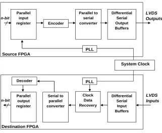
3.4.1 LVDS Signaling ...29
3.4.2 SERDES Architecture ...31
3.4.3 SERDES Multiplexing ...33
3.5 Multi-Gigabit Transceiver (MGT) ...35
3.5.1 CML Signaling ...35
3.5.2 MGT Architecture ...36
3.5.3 MGT Multiplexing ...39
3.6 Comparison of Three Multiplexing Schemes ...42
3.7 Previous Research on MFS multiplexing ...43
3.8 Summary ...47
Chapter 4 Optical Interface in MFS 4.1 Introduction ...48
4.2 Short-Range Optical Interface ...49
4.2.1 Optical Fibers ...50
xi
4.3 MFS Serial Optical Interface ...60
4.4 Proposed Latency-Optimized 2D MFS with Optical Interface ...61
4.4.1 Proposed Architecture ...61
4.4.2 Multiplexing in Proposed Architecture ...65
4.4.3 Evaluation Strategy ...65
4.5 Previous Research on MFS Serial Optical Interface ...65
4.6 Summary ...71
Chapter 5 Optical 3D MFS Routing Architectures 5.1 Introduction ...72
5.2 Why 3D MFS Architecture ...73
5.2.1 Interconnection Length Distribution ...73
5.2.2 Asymptotic Behavior of Wire-length ...74
5.2.3 Structural Distribution & Placement Optimization ...76
5.3 Proposed 3D MFS Architecture ...76
5.3.1 Motivation ...76
5.3.2 Proposed 3D Optical MFS Routing Architectures ...77
5.3.3 Multiplexing in 3D Routing Architectures ...79
5.3.4 Evaluation Strategy ...80
5.4 Previous Research on 3D MFS ...81
5.5 Summary ...83
Chapter 6 CAD Tools and Experimental Evaluation Framework 6.1 Experimental Design Mapping Flow ...84
6.2 Assumptions ...86
6.2.1 FPGA Pin Assignment ...86
6.2.2 Intra-FPGA Placement and Routing ...87
6.3 CAD Tools ...87
6.3.1 ABC Tech-Mapper ...87
6.3.2 Translator ...88
6.3.3 Multi-way Partitioning ...88
xii
6.3.5 MFS Timing Analyzer ...91
6.3.6 Time-Multiplexed Inter-FPGA Router ...94
6.4 Evaluation Metric...95
6.4.1 Emulation Time and System Frequency ...95
6.5 Benchmark Circuits ...96
6.6 Summary ...97
Chapter 7 Experimental Results and Comparison of Architectures 7.1 Introduction ...98
7.2 Comparison of Multiplexed Routing Architectures ...98
7.2.1 Critical Path Delay ...98
7.2.2 System Frequency ...102
7.3 Comparison of Proposed 2D Optical & Conventional MFS ...106
7.3.1 Critical Path Delay ...106
7.3.2 System Frequency ...107
7.4 Comparison of Proposed 3D Optical & Conventional MFS ...115
7.4.1 Critical Path Delay ...115
7.4.2 System Frequency ...117
7.5 Summary ...125
Chapter 8 Conclusions and Future Work 8.1 Dissertation Summary ...127
8.2 Principal Contributions ...129
8.3 Future Directions ...130
References ...131
xiii
LIST OF FIGURES
1.1 Multi-FPGA Board;DN7020K10 (DiniGroup) ...2
2.1 Hard-wired MFS (DNV7F4A) ...9
2.2 Photograph of 2 TwinStar FPGA Systems ...10
2.3 Synopsys’ HapsTrak 3 Connector Technology ...11
2.4 Routing Architectures (a) CCG, (b) TORUS ...14
2.5 The AnyBoard System ...15
2.6 (a) Basic Mesh Architecture (b) 8-way Mesh (c) One-Hop Mesh ...17
2.7 Maxwell FPGA Connectivity ...19
2.8 (a) Full Crossbar (b) Partial Crossbar ...20
2.9 BEE2 System Topology ...21
2.10 HCGP Architecture ...22
3.1 Critical Path Delays ...27
3.2 Logic Multiplexing Scheme ...28
3.3 LVDS Architecture ...30
3.4 Generic SERDES Architecture ...32
3.5 SERDES Multiplexing Scheme ...33
3.6 CML Architecture ...36
3.7 Multi Gigabit Transceiver Architecture ...38
3.8 MGT Multiplexing Scheme ...40
3.9 NoC Emulation Board...44
4.1 Optical Interface Evolution ...49
4.2 (a) Single-Mode (b) Multi-Mode Optical Fiber Core Dimensions ...52
4.3 Optical Transmitter Block Diagram ...55
4.4 Optical Receiver Block Diagram ...56
4.5 Optical FPGA &Transceivers ...58
4.6 Simplified inter-FPGA serial optical interface structure ...61
xiv
4.8 Demonstrator design with the 3 optoelectronic FPGA chips and encapsulated
Optical pathway ...63
4.9 Samtec FireFly™ Micro Flyover System ...64
4.10 High level view of the hardware setup ...66
4.11 Block Diagram ...69
4.12 Block diagram of remote configuration on LTDB Demonstration ...71
5.1 Comparison of interconnection length distribution for 2D & 3D architectures ....74
5.2 Possible Combination Classes in 3D (a) A-combination (b) N-combination (c) R -combination...75
5.3 2D MFS Architecture ...77
5.4 3D MFS topologies with various degrees of optical interconnect ...78
6.1 Design Flow for Time-Multiplexed MFS ...85
7.1 Number of Inter-FPGA nets After Partitioning ...99
7.2 System Frequency vs Multiplexing Ratio ...102
7.3 System Frequency 2D Conventional vs Optical MFS in CCG & TORUS ...108
7.4 System Frequency Gain 2D Optical vs Conventional MFS in CCG & TORUS .112 7.5 Average System Frequency Gain 2D Optical vs Conventional CCG & TORUS 115 7.6 System Frequency 2D vs 3D with MGT Multiplexing Scheme ...118
7.7 System Frequency Gain 2D vs 3D with MGT Multiplexing Scheme ...121
xv
LIST OF TABLES
3.1 Comparison of LVDS & CML ...36
3.2 Latency Values of GTY TX & RX Blocks ...41
3.3 Comparison of 3 Multiplexing Schemes...42
4.1 Comparison between MMF & SMF ...53
6.1 Delay Values Used in Static Timing Analyzer ...92
6.2(a) Benchmark Circuits ...96
6.2(b) Benchmark Circuit ...97
7.1 KaFFPaE Partitioning Results ...99
7.2 Threshold Multiplexing factor (muxthreshold) for Multiplexed Routing MFS ...100
7.3 Critical Path Delays (in nanoseconds) at Different levels of Circuit Implementation for 2D MFS ...101
7.4 Critical Path Delays (in nanoseconds) at Different levels of Circuit Implementation for 2D MFS ...106
7.5 Critical Path Delays (in nanoseconds) at Different levels of Circuit Implementation for 2D Optical MFS ...107
xvi
LIST OF ABBREVIATIONS
2D Two-dimensional
3D three-dimensional
ASIC Application Specific Integrated Circuit
CCG Completely Connected Graph
CLB Configurable Logic Block
CML Current Mode Logic
CPD Critical Path Delay
CPU Central Processing Unit
DSP Digital Signal Processing
EMI Electro-magnetic Interference
FPGA Field Programmable Gate Array
FPID Field Programmable Interconnect Device
Gbps Giga bits per second
GHz Giga Hertz
HPC High Performance Computing
IC Integrated Circuit
InP Indium Phosphide
I/O Input / Output
KaHIP Karlsruhe High Quality Partitioning
LUT Look-Up Table
LVDS Low Voltage Differential Signaling
MFS Multi-FPGA System
MHz Mega Hertz
MGT Multi Gigabit Transceiver
MMF Multi Mode Fiber
PCB Printed Circuit Board
PLL Phase Locked Loop
PMMA Ploy Methyl Methacrylate
POF Plastic Optical Fiber
xvii
SERDES SERializer / DESerializer
SFP Small Form-Factor Pluggable
SMF Single Mode Fiber
SoC System on Chip
STA Static Timing Analyzer
TDM Time Division Multiplexing
THz Tera Hertz
TX Transmitter
1
Chapter 1 Introduction
1.1. Multi-FPGA System (MFS)
Today’s general purpose microprocessors are optimized for general purpose applications.
This implies that the user has to optimize his code for the processor as it is physical
predefined silicon that cannot be modified to fit to user’s application. Custom ICs for
specific applications such as encryption use hardware that cannot be changed after
fabrication. The Field Programmable Gate Array, in short "FPGA", is different. This chip
allows the user to modify the silicon through software configuration to be the ideal
Application Specific Circuit or short "ASIC" for user defined application, while remaining
reconfigurable. Currently, a few to tens of such FPGAs are used for emulating millions of
logic gates and for accelerating computationally intensive applications. Super computer
level performance can be achieved at a fraction of the cost for high performance computing
(HPC) applications.
Multi-FPGA systems are an important area of research. These systems connect multiple
FPGAs in a fixed pattern, to implement complex logic circuits as shown in Figure 1.1.
They offer the potential to deliver higher performance solutions to general computing tasks,
logic emulation, rapid prototyping and reconfigurable custom computing machines [1].
Multi-FPGA boards for ASICs prototyping and High Performance Computing (HPC)
enable high-speed, accurate prototyping and emulation, system and IP design. “These
platforms also facilitate sub-microsecond latency market data processing and order
execution and allow orders of magnitude higher performance for algorithmic trading as
well as options pricing and risk management, over conventional software-based and hybrid
approaches” [85]. MFS designed for individual applications can be further optimized by
the type of FPGAs and interconnections employed.
In addition to FPGAs, almost all MFSs have memory chips and other devices such as
CPUs, Ethernet ports, expansion slots, External Clock inputs / outputs (I/Os) and DSP
2
example, the commercial platform DN7020K10 configured with 20 Intel/Altera Stratix
4SE820s can emulate up to 130 million logic gates [23].
Figure 1.1: Multi-FPGA Board; DN7020K10 (DiniGroup) [23]
SciEngines offers RIVYERA S6-LX150; a 128 Xilinx Spartan-6 LX150 FPGA cluster
with external memory and CPU cores representing high performance reconfigurable
platforms [3].
However, there are multiple factors that must be taken into account in a multi-FPGA design
to achieve desired performance from these systems.
1.2.
Multi-FPGA System Constraints
1.2.1. Pin Limitation Problem
The first constraint of an MFS is the limited number of I/O pins. Over the past few years,
the logic capacity per FPGA is increasing at a much faster pace as compared to the number
of I/O pins. Large SoCs may not be routed among multiple FPGAs without overflowing
the available I/O resources of a single FPGA [5]. Mapping a design to an MFS is mainly
divided into two steps. In the first step, the design is partitioned into several parts. A
3
single FPGA in MFS. The second step routes the inter-FPGA nets according to the
available physical tracks, I/O resources of the FPGA and the routing architecture of MFS.
But, out of these available pins, some need to be reserved for non-FPGA connections and
in case of differential signaling, some need to be reserved to propagate the clock instead of
the user data. Consequently, the number of available pins for inter-FPGA data
communication is further decreased. One of the solutions to this issue can be to alter the
partitioning of the design which can change the number of inter-FPGA nets [6]. However,
re-partitioning does not solve the problem in every design.
1.2.2. Off-Chip Communication Strategy
Although MFSs are capable of accommodating large designs, their off-chip
communication strategy imposes bandwidth constraints and limits the overall system
performance [1, 4]. The selection of the MFS routing architecture exercises considerable
effect on the critical path delay and system frequency of a design. The routing architecture
of an MFS is the manner in which the FPGAs, fixed wires and/or programmable
interconnect chips are connected together. In certain routing topologies providing full
connectivity, signals can be routed from source FPGA to its destination FPGA via direct
off-chip connections without any interference. However, in other routing architectures,
sometimes the signals need an intermediate FPGA or a route-through to reach the
destination FPGA. In such a case, the signal is sent into one pin of the route-through FPGA,
through the on-chip routing and then out through the other pin, without using any of the
on-chip logic. Such inter-FPGA nets inflict even larger delays than the direct connections
and adversely affect the system frequency. Since the I/O pin and off-chip routing delays
are much larger than the on-chip delays in an MFS, that’s why the speed of the
implemented design is primarily dictated by them. Moreover, the routing resources
consume significant board area and scaling up an MFS only aggravates the latency, area
and cost issues. Therefore, selection of the appropriate routing architecture is vital in
4
1.2.3. Inter-FPGA Interface Selection
Over the last few decades, applications’ data bandwidth requirements are constantly
increasing which demand a compatible high-speed interface capable of maintaining
multi-gigabits data rate. Generally, designers employ copper interconnect for chip-to-chip and
chip-to-module interfaces over traces on a printed circuit board (PCB). However, copper
based interconnects are incapable of scaling up with the data rate due to the frequency
dependent losses. For instance, FR-4 copper trace material suffers from a loss of ~ 0.5-1.5
dB/inch at 5 GHz (Nyquist for 10 Gbps rate), and the loss increases to ~ 2.0-3.0 dB/inch at
12.5 GHz (Nyquist for 25 Gbps rate) [7]. Maximum bandwidth is also limited by return
loss, insertion loss and crosstalk. In present technology, designers use copper electrical
interface in MFS, however, at multi-gigabit data rates, inter-FPGA electrical
interconnections are restricted in their performance due to signal integrity, latency, power
and cost issue. Therefore, designers are exploring the idea of applying short-range optical
fiber signaling in order to overcome these challenges.
Unlike copper interfaces, optical fiber has virtually no loss and its power consumption and
penalty is relatively independent of reach length, Moreover, optical interface is immune to
electromagnetic interference (EMI) and does not have amplitude crosstalk, resulting in
better signal integrity resilience. Replacing PCB traces with an optical interface in MFS
can provide significant power, resource, and cost reductions. Thus, the choice of off-chip
interconnection type at very high data rates can determine the latency, bandwidth, area and
cost constraints in an MFS.
1.3.
Thesis Goals
Performance of existing MFS routing architectures is limited by many factors as discussed
earlier: limited pin resources, inter-FPGA communication strategy and off-chip interface
selection. This research is aimed at addressing the constraints of existing MFSs and
optimizing their performance by proposing new models. We have developed CAD tools
for experimentally evaluating and comparing existing and proposed time-multiplexed MFS
5
• The first goal is to enable the MFS to accommodate large design which exceed the
I/O pin and logic capacity of an FPGA. The proposed solution is to implement
multiplexing and study the behaviour of MFS system frequency with respect to
increasing multiplexing ratio in three different multiplexing schemes.
• Next goal is to investigate the effects of different routing architectures on the system frequency of an MFS.
• In the next part of this research, our goal is to improve the system frequency by
decreasing the off-chip latencies in an MFS. In order to achieve this objective, we
proposed latency-optimized planar 2D MFS architectures in which electrical
interconnections are replaced by optical interface in same spatial distribution. • Lastly, we aim at achieving improved MFS system frequency with smaller footprint
area. For this, we proposed 3D MFS architectures with vertical stacking and optical
off-chip interfaces.
1.4.
Thesis Contributions
In order to resolve the problems stated above, the major contributions of this thesis include
the following:
• We have proposed novel scalable 3D MFS architectures which showed improved
system performance as compared to conventional 2D MFS architectures. The
vertical stacking resulted in shorter off-chip links improving the overall system
frequency with the additional advantage of smaller footprint area.
• The proposed 3D architectures employed serialized interconnect between
intra-plane and inter-intra-plane FPGAs to address the pin limitation problem. Additionally,
all off-chip links are replaced by optical fibers that exhibited latency improvement
and resulted in faster MFS. Results indicated that exploiting third dimension
provided latency and area improvements as compared to 2D MFS. The
experimental results have shown average 37% improvement in system frequency
as compared to planar MFS with electrical interconnects.
• We also proposed latency-optimized planar 2D MFS architectures in which electrical interconnections are replaced by optical interface in same spatial
6
architectures exhibited reduced critical path delay and system frequency
improvement as compared to conventional MFS. 2D optical platforms exhibited an
average frequency gain of 22% as compared to 2D MFS with electrical
interconnects.
• Achieved performance of three time multiplexing schemes; Logic Multiplexing,
SERDES and MGT, is compared for a given range of multiplexing ratio using
different routing architectures in planar MFSs with PCB connections.
1.5.
Thesis Organization
The rest of the thesis is organized as follows:
Chapter 2 studies the two multi-FPGA routing architectures i.e. Completely Connected
Graph (CCG) and TORUS. It describes the two architectures’ performance with electrical
and optical interface in both 2D and 3D topologies. Then, the previous work done regarding
MFS routing architectures is discussed in detail.
Chapter 3 focuses on the three multiplexing schemes i.e. Logic Multiplexing, SERDES and
MGT, their detailed description and comparison. Then the relationship between the system
frequency and the multiplexing ratio is explained and derived, and finally, the previous
work done in time multiplexed MFS is presented.
Chapter 4 describes the characteristics of short-ranged optical interface and its detailed
design and application in MFSs. The chapter also covers the previous research done on this
topic.
Chapter 5 explains the proposed 3D MFS architectures with optical interface. The
feasibility, practicality and advantages of vertically stacked MFS are discussed in detail
and also the past research done on the subject is also presented.
Chapter 6 explains the framework employed for experimental evaluation of MFS routing
architectures. The experimental procedure and customized set of mapping tools used for
7
comparing multiplexed architectures are explained and the details of the benchmark
circuits are also presented.
Chapter 7 compares the achieved performances for a set of designs mapped on the two
multi-FPGA platforms employing three multiplexing schemes. The performance gains
between these platforms are quantified. Then, the performance comparison is drawn
between 2D MFS with multiplexed electrical interface and the proposed 2D MFS with
optical interface. Lastly, we have drawn a comparison between 3D MFS with serialized
optical interface and 2D conventional MFS.
8
Chapter 2 MFS Routing Architectures
2.1.
Inter-FPGA Connections & Routing
Multi-FPGA systems require chip-to-chip connections and there are several ways to
organize these inter-chip connections. The routing architecture of an MFS is the manner
in which the FPGAs, fixed wires and/or programmable interconnect chips are connected
together. The routing architecture exercises a strong effect on the cost, speed and routability
of the system [1]. Other than the inter-FPGA connection arrangement, the type of
connectors employed is also an integral part of MFS routing architecture and impact the
overall system performance [8].
2.2.
Types of Inter-FPGA Connections
2.2.1.
Hard-wired ConnectionMFS with hard-wired connections consists of a ready-made generic multi-FPGA board,
where all the inter-FPGA connections are fixed and realized using PCB traces. The
connections to external interfaces are fixed as well, however these connections can be
realized using PCB traces or connectors. One of the examples of such platform is the
commercial DNV7F4A platform as shown in Figure 2.1, by Dini Group [2]. This platform
is made up of four Virtex-7 FPGAs with all fixed FPGA to FPGA interconnects (either
differential or single-ended).
Some of other major existing commercial off-the-shelf platforms with hard-wired
connections are as follows:
• Cadence Protium Rapid Prototyping Platform [9],
• S2C 6th generation prototyping hardware with four Xilinx Kintex UltraScale XCKU115 FPGAs
• Quad KU115 Prodigy Logic Module [10]
• BEECubeBEE7 off-the-shelf communications platform with four Xilinx VX690T
9
• HyperSilicon VeriTiger-DH2000TQ prototyping board with two Xilinx Virtex-7
FPGA devices [12].
Figure 2.1: Hard-wired MFS (DNV7F4A) [2]
MFS with hard-wired connections can also be customized by tailoring the inter-FPGA
connections according to the design requirements.
2.2.2. Cabling Connection
MFS with cabling connections is a relatively new technology consisting of multiple
ready-made FPGA devices connected by cables and connectors. The FPGA-FPGA connections
as well as the FPGA-external interfaces can be inserted or eliminated merely by connecting
or disconnecting the cables with or from the connectors to meet the design requirements.
MFS with cabling connections exhibits properties of both off-the-shelf and custom boards,
because it employs generic ready-made devices while allowing changeable inter-FPGA
connections by connecting or disconnecting the cables in order to be tailored according to
10
One of many examples of such connections is proFPGA quad V7 multi-FPGA system
which provides flexible and scalable FPGA interconnection structure with high-speed
connectors and cables. These specific high speed connectors allow maximum point to point
speed of up to 1.8 Gbps over the standard FPGA I/O and up to 12.5 Gbps over the high
speed gigabit transceiver pins of the given FPGA. The high interconnection flexibility
offers the designer a maximum speed of his/her design running in the proFPGA system.
Furthermore, multiple proFPGA quad or duo systems can also be stacked or connected
together resulting in unlimited scalability and no theoretical maximum in capacity [13].
Figure 2.2: Photograph of 2 TwinStar FPGA Systems [14]
Similarly, IBM’s Twinstar system was configured with 24 node cards and used 45
XilinxVirtex-5 LX330 FPGA devices, in addition to the control FPGA devices and discrete
SRAM and DRAM components [14]. As shown in Figure 2.2, it was constructed with
flexible cable interconnect structure facilitating multiple connection topologies. The Active
Backplane provided flexible interconnect with high-speed LVDS-based point-to-point
communication links. Synopsys’ HAPS-70 FPGA-based prototyping platforms [15] is
built with HapsTrak 3 interconnect cables (Figure 2.3) for high speed interconnectivity
11
connector meets the specific requirements of FPGA-based prototyping and high-speed
interface via HAPS interconnect cables.
Figure 2.3: Synopsys’ HapsTrak 3 Connector Technology [15]
2.2.3. Optical Connection
Reach length, power, cost, board material, and circuit board complexity are major
challenges for copper based, chip-to-chip interfaces. Replacing on-board cabling or
hard-wired connections by optical interface on MFS overcomes the limits of copper interconnect
by integrating the latest FPGAs with state of the art photon propagation properties,
providing reach-length, power, cost, density, and bandwidth advantages. Short-ranged
chip-chip optical interconnection not only offers design flexibility like cabling connection,
but also dramatically exceeds conventional electrical signaling and interconnects
capabilities. As data rates exceed 10 Gbps and higher, optical interface technology
overcomes bandwidth challenges encountered by conventional copper connections.
Further details on the multi-FPGA boards with optical interface are provided later in the
thesis.
2.3.
MFS Routing Architectures
MFS interconnect topology influences the overall speed and performance of the system.
Researchers have proposed many 2D routing architectures over the years and empirically
12
not Field Programmable Interconnect devices (FPIDs) or crossbars are used for connecting
the FPGAs. If FPIDs are not used, it is referred to as an FPGA-only architecture.
MFS routing architectures explored in this research are Completely Connected Graph
(CCG) and TORUS. The architectural issues and assumptions that arise when mapping real
circuits to these architectures are discussed in detail below.
2.3.1. Basic Assumptions
Following assumptions are made for this research:
• First assumption for this research is that the MFS architectures explored are
homogeneous, in which a single type of FPGA is utilized. Heterogeneous platforms
using FPGAs of different sizes are achievable however rarely used, and are restricted
to application-specific (custom) MFSs. In our 2D and 3D architectural models, the chip
size is considered to be a fixed parameter. Therefore, instead of adapting the chip size,
the number of chips is increased or decreased according to the design requirements.
• Another important issue is the choice of FPGA. The FPGA used in this research is the
Xilinx Kintex Ultrascale+ FPGA KU3P, which consists of 163,000 6-LUTs and
325,000 flip-flops. The chosen FPGA offers 16 GTY transceivers with 32.75 Gbps
inter-FPGA communication data rate. GTY transceiver supports small form-factor
pluggable (SFP) or SFP+ optical module required for off-chip optical interface. In
terms of logic capacity and data rates, KU3P is one of the latest and fastest available
FPGA in the market. Since the FPGA employed has enormous logic capacity that is
why we have chosen the largest available real benchmark circuits. Large benchmark
circuits not only stress the FPGA capacity but also the CAD tools developed for the
purpose of experimental evaluation of 2D and 3D architectures.
• We have considered point-to-point connections in all the MFS architectures.
Point-to-point connections connect two FPGAs directly to each other. After partitioning, the
design is divided into several parts. All 2-point and multi-point inter-FPGA nets are
routed in MFS point-to-point connections. Multi-terminal nets are split into several
2-terminal nets. This assumption is valid because we have employed multiplexing, which
13
• Another assumption is that the CAD tools developed are designed to handle
synchronous mode where entire system uses a single global clock. There are two
distinct types of time-multiplexing implementations: synchronous and asynchronous.
In synchronous mode, the multiplexing clock and the system clock are synchronous.
Whereas, in asynchronous mode, the multiplexing clock runs completely independent
of the system clock and can supports multiple clocks.
Some commercial tools available for single-FPGA static timing analysis can handle
asynchronous mode and in future, this research can be extended by developing static timing
analysis tool using multiple clocks to build an asynchronous system.
2.3.2. 2D and 3D MFS Routing Architectures
The simplest 2D mesh topology can be designed with each FPGA connected to its
horizontal and vertical adjacent neighbors. Mesh architecture provides full connectivity
and any combination of connections between inputs and outputs can be made. The number
of traces connecting adjacent FPGAs depends upon the number of I/O pins available per
FPGA. Xilinx KU3P FPGA has 208 High-Performance (HP) single-ended I/O pins. Out of
these, 3 pairs are reserved for non-FPGA connections and 25 pairs are for the primary I/O
signals. The connections to external interfaces can be realized using hard-wired PCB traces
or connectors and cables. Therefore, 152 pins are left for inter-FPGA connections. All
FPGA-FPGA interconnects can be routed as LVDS or single-ended according to the design
requirements. In case of SERDES differential signaling, one pair of pins between every
FPGA pair has to be reserved to propagate the clock instead of the user data and these pins
should be clock capable.
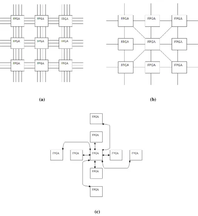
Completely Connect Graph (CCG) is a topology in which all the FPGAs are connected to
each other as shown in Figure 2.4 (a). Since, the MFS size is set to be 6 in this research and
the available pins per FPGA are 152, this implies that there are ⌊152/5⌋ tracks between
any pair of FPGAs on the board.
In TORUS architecture each FPGA is connected only to its horizontal and vertical adjacent
neighbors. Moreover, the peripheral FPGAs are wrapped around in horizontal and vertical
14
Figure 2.4 (b). For an MFS size of 6, each FPGA is connected to maximum 3 neighbors in
TORUS and each edge in Figure 2.4 (b) represents ⌊152/3⌋ tracks between any pair of
FPGAs.
Figure 2.4: Routing Architectures (a) CCG, (b) TORUS
In case of vertically stacked MFS, the FPGA interconnection topologies of CCG and
TORUS remain the same as that in planar platforms. 3D architectures are discussed in
detail later in the thesis.
2.4.
Previous Research on MFS Routing Architectures
In this section we will look at the different routing architectures proposed over time in
MFSs. The existing routing architectures can be categorized roughly in the following three
categories: linear arrays, meshes and architectures that employ programmable interconnect
chips. The first two types are the examples of FPGA-only architectures.
2.4.1. Linear Arrays
FPGAs are arranged in the form of a linear array in this type of architecture, which is
appropriate for one-dimensional systolic processing applications. This architecture has
very restricted routing flexibility and numerous designs may run out of routing resources
15
certain niche applications, its utility as a general purpose MFS is extremely limited. Two
historically recognized examples of this architecture are AnyBoard [16] and Splash [17].
As shown in Figure 2.5, the AnyBoard system employs five Xilinx 3090 FPGAs and three
128K x 8 RAMs.
Figure 2.5: The AnyBoard System [16]
Adjacent Xilinx chips in the array are connected through local buses that offer
communication between function blocks in systems. FPGAs located at the opposite ends
of the array are connected to structure a ring topology and all the FPGAs are attached to a
global bus. An extension of the global bus with dedicated I/O lines from each FPGA
provides the system interface. This can be utilized for routing I/O signals of the circuits.
The control FPGA is employed to implement circuitry for managing the PC bus interface,
FPGA configuration management and hardware debugging support. The idea of using the
control FPGA is to leave all the logic in other FPGAs for implementing the required design
functionality. The AnyBoard system was one of the first MFSs built for accelerated
prototyping of small designs. It was an economical system that demonstrated the
prospective of MFSs as an attractive and low-cost means for rapid prototyping of scores of
16
The Splash logic-array board has 32 Xilinx 3090 programmable gate arrays and 32 memory
chips. Two additional Xilinx chips are used for bus control. The Splash design was
motivated by a systolic algorithm for DNA pattern matching [17].
Cube [25] was massively-parallel FPGA architecture with 512 FPGAs connected in
systolic chain with identical interfaces between them. Each module in the Cube platform
hosted 64 Xilinx FPGAs arranged in an 8 by 8 matrix. Eight FPGAs were grouped together
in a row and had independent configuration inputs and power supplies. The complete
system consisted of 8 connected boards in a cabinet forming an 8×8×8 cluster of 512
FPGAs, and therefore named Cube.
2.4.2. Mesh Architectures
In the basic design of mesh architecture, the FPGAs are placed in the form of a
two-dimensional grid with every FPGA connected only to its four nearest neighbors as shown
in Figure 2.6(a). In this manner, the FPGAs are stitched together into a single, larger
structure, with the Manhattan distance measure that is representative of most FPGAs
carried over to the complete array structure.
In order to decrease the average number of I/O pins required to route signals and improve
the routability, we can increase the number of neighbors linked to an FPGA. Rather than
the simple four-way basic connection pattern of Figure 2.6(a), we can implement an 8-way
topology, Figure 2.6(b). In the eight-way architecture, an FPGA is not only connected to
those FPGAs horizontally and vertically adjacent, but also to those FPGAs which are
diagonally adjacent. A second option is a one-hop topology, Figure 2.6(c). In this
arrangement, an FPGA is linked to the two nearest FPGAs directly above, below, to the
right, and to the left. Two-hop, three-hop, and longer connection patterns have also been
considered [18]. In Figure 2.6(b) & (c), each line between any pair of FPGAs represent
multiple number of traces and depends upon the available FPAG I/O pins.
The benefits of mesh are simplicity of local interconnections and straight forward
scalability. However, using FPGAs for interconnections lessens the number of pins for
17
large between widely separated FPGAs (especially in bigger arrays) whereas those between
neighboring FPGAs are minute. The outcome is degraded speed performance and timing
problems such as setup and hold time violations because of widely variable interconnection
delays. Quickturn RPM [19], DEC PeRLe-1 [20], and the MIT Virtual Wires project [21]
are a few examples in this category.
(a) (b)
(c)
Figure 2.6: (a) Basic Mesh Architecture (b) 8-way Mesh (c) One-Hop Mesh
The Quickturn RPM Emulation System had FPGAs hardwired together on large
18
array of signal-routing channels. The routability and speed problems of the mesh
architecture that arose when implementing general logic circuits, forced Quickturn to
switch to a superior architecture (partial crossbar) in their next generation logic emulation
systems.
Virtual wires got rid of the pin limitation problem of prior emulators by intelligently
multiplexing each physical wire amongst numerous logical wires, and pipelining these
connections at the highest clocking frequency of the FPGA. Consequently, the available
off-chip communication bandwidth was increased by multiplexing the utilization of FPGA
pin resources (physical wires) among multiple emulation signals (logical wires).
By employing virtual wires scheme on a mesh, low-cost logic emulation was achieved
because in expensive low pin count FPGAs were used and the mesh architecture was
reasonably simple to be manufacture. On the other hand, the drawbacks were the speed
penalty and increased mapping software complexity due to pin multiplexing. Moreover, in
certain cases it might not be easy to map sections of asynchronous logic that might be
present in the circuit to be emulated since asynchronous signals could not be assigned to a
specific time slice (phase) in the emulation clock period.
The mesh topology also performed well when implementing algorithms which matched its
architecture. This was established convincingly by the DEC PeRLe-1 system which used a
4-way mesh consisting of 16 Xilinx 3090 FPGAs along with 7 control FPGAs, 4 MB of
static RAM, four 64-bit global buses and FIFO devices. The said system gave superior
performance and cost in contrast to every other contemporary technology of its time,
including supercomputers, massively parallel machines, and conventional custom
hardware for various applications, including cryptography, high energy physics, image
analysis and thermodynamics.
Maxwell [24] used a 2-D TORUS routing architecture between 64 FPGAs to demonstrate
its effectiveness for high-performance computing applications. The FPGAs used in
Maxwell were Xilinx Virtex-4 devices in two flavors. Alpha Data cards used XC4VFX100,
while Nallatech cards used XC4VLX160. Xilinx’s LX Virtex range offered greatest
19
(“RocketIO”) for off-chip communications. These two types of Virtex-4 FPGAs were built
into two flavors of plug-in PCI card: the Nallatech H101 and the Alpha
DataADM-XRC-4FX. Both types of card were connected using a PCI/PCI-X bridge. The FPGA network
consisted of purely point-to-point links between the MGT connectors of adjacent FPGAs
and did not implement routing logic in the FPGA devices. The MGTs were connected with
standard Infiband cables of 50cm and 100cm lengths, kept as short as possible.
Figure 2.7: Maxwell FPGA Connectivity [24]
Catapult [26] was built on a two dimensional 6X8 network topology, which balanced
routability and cabling complexity. The inter-FPGA network requirements were low
latency and high bandwidth and therefore the traces were routed through mezzanine
connector between daughtercard and mothercard. Note that it is a not strictly an MFS
because each FPGA worked independent of the other.
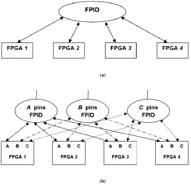
2.4.3. Programmable Routing Architectures
In this type of architecture, all the interconnections among FPGAs are routed through Field
Programmable Interconnect devices (FPIDs). A superlative model of this architecture
would be a full crossbar that employs a single FPID for linking all FPGAs, as shown in
Figure 2.8(a). However, the complexity of a full crossbar increases as a square of its pin
count and therefore it is limited to systems that have at most a few FPGAs. A brief review
20
Aptix FPIC device [22] was the first FPID brought into the market. Each FPIC had 1024
pins arranged in a 32 x 32 I/O pin matrix. Every pin was connected to two I/O tracks that
orthogonally crossed the routing channels. Each routing channel consisted of sets of
parallel tracks that were segmented into a variety of sizes to hold different signal paths with
different lengths. Bidirectional pass transistors which were controlled by SRAM cells
connected I/O tracks to routing tracks and routing tracks to other routing tracks.
(a)
(b)
Figure 2.8: (a) Full Crossbar (b) Partial Crossbar
Through selectively programming the SRAM cells, the user could connect any device pin
to any number of other pins
The partial crossbar architecture shown in Figure 2.8(b) overcomes the limitations of the
21
FPGAs and three FPIDs and the pins in each FPGA are divided into N subsets, where N is
the number of FPIDs in the architecture. All the pins belonging to the same subset in
different FPGAs are connected to one FPID. The number of pins per subset determines the
number of FPIDs needed and the pin count of each FPID. Delay through all inter-FPGA
connections is uniform and the size of the FPIDs increases linearly as a fraction of the
number of FPGAs.
2.4.4. Tree Topology
A tree routing topology in a MFS resembles the structure of a directed acyclic graph, in
which every node except the root node has exactly one incoming edge, and no node has
more than n outgoing edges where n is the arity of the tree. Such a tree is usually referred
to as an ‘n-ary tree’. In the MFS implementation, every edge is considered implicitly
bidirectional. For compact trees, tree depth 𝑑 = ⌈log𝑛𝑚⌉, where m is the number of leaf
nodes. Symmetry exists at every child-bearing node in this tree topology. Obviously,
increasing n would increase the symmetry of the overall system. However, when n = m and
d= 1, the tree reduces to the crossbar. The usual purpose of having a tree structure with
n<m is to reduce the overhead of implementing the system.
Figure 2.9: BEE2 System Topology
Berkeley emulation engine II (BEE2) [27] proposed a basic structure with a set of modules,
each of which were implemented as a tree of fixed d and n. The root FPGAs of the modules
22 n = 4 was selected, as it appeared to be the largest number of edges that could be supported
by a single FPGA. The system resulted in an m/4-way crossbar that was easily implemented
using off-the-shelf infiniband switches even for m > 256. The overhead of the BEE2 turned
out to be about 1/16 that of a full crossbar.
2.4.5. Other MFS Routing Architectures
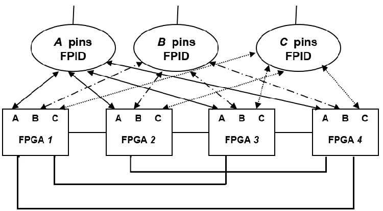
Khalid et al. [1] proposed the hybrid complete-graph and partial-crossbar (HCGP) routing
architecture that used both hard-wired and programmable connections between the FPGAs.
The proposed architecture was similar to partial crossbar, with the added feature that the
router exploited the direct connections between FPGAs to minimize the number of FPGA
and FPID pins used for routing and to minimize the net delay for critical inter-FPGA nets.
The proposed architecture produced superior results as compared to partial crossbar in
terms of speed and pin cost.
Figure 2.10: HCGP Architecture
The HCGP routing architecture for 4 FPGAs and 3 FPIDs is shown in Figure 2.10. The I/O
pins in each FPGA were divided into two sets: hardwired connections and programmable
connections. The pins in the first set were connected to other FPGAs and the pins in the
second set were connected to FPIDs. The FPGAs were directly connected to each other
23
connections between FPGAs were evenly distributed, i.e. the number of wires between
every pair of FPGAs was the same.
The FPGAs and FPIDs were connected in the same manner as that in a partial crossbar
which meant that any circuit I/O had to go through FPIDs to reach FPGA pins. That’s why,
a certain number of pins per FPID were reserved for circuit I/Os. Using FPID for routing
multi-terminal nets helped tackle that scares pin resources of an FPGA in HCGP.
In 3D domain, [4] proposed a three-dimensional concentric 4-FPGA routing architecture
resulting in equal length concept between FPGA pins enabling wave-pipelined
pin-multiplexing. This research concentrated on switch based routing and used pass transistor
as logic element for switching technology due to its speed advantage and bidirectional
functionality compared to buffer based technology. Pass transistor has a propagation delay
of 0.1ns however; it has the disadvantage of degrading the slope of the signal over multiple
switches. Since, the circuit behavior heavily depended on the capacity of the board traces,
that’s why the impact was kept minimal by using short connections. The connections
between FPGAs and non-FPGA devices were kept fixed, whereas the inter-FPGA
connections were mapped on the existing hardware. The switches were mounted on a
specific switch-board which connected vertically with two adjacent FPGA boards. Besides
the connectivity to the switch network, every FPGA pin was routed to external connectors
to be accessed by non-FPGA devices. The author suggested that the main advantage of this
concept was that any possible signal connectivity could be routed on the proposed structure
and unused or additional pin penalty did not occur. The second advantage of this routing
concept was the equal length of the connectivities which meant in this context a difference
of less than 5 millimeters. Therefore, all signal connections from one FPGA to any other
FPGA passed the same number of switches and had the same length. However, the author
considered randomly generated designs instead of real benchmarks to evaluate the
performance of the proposed architecture.
2.5. Summary
A review of different types of inter-FPGA connections in existing MFSs and the different
24
categorized as hard-wired, cable connections or optical interface. Depending upon the
interconnection structure, MFSs can be grouped into three main categories; linear arrays,
meshes, and architectures that use programmable interconnection chips. Relevant MFS
architecture research studies were also discussed in this chapter. The chapter also presented
the two routing architectures employed in this research i.e. CCG (Completely Connected
Graph) and TORUS. Both routing architectures were discussed in context with 2D and 3D
25
Chapter 3 Time Multiplexing in MFS
3.1. Introduction
Large SoCs may not partition into multiple FPGAs without over flowing the available I/O
resources. One of the possibilities to make the design routable is by changing the way that
logic is partitioned into multiple FPGAs, since partitioning can alter the number of
inter-FPGA nets going between partitions. However, repartitioning is not always an effective
solution. Rising levels of chip functionality and data throughput requirements have
persuaded the chip industry in migrating from inferior data rate parallel connections to
higher speed serial connections. Employing high speed serial interface not only resolves
limited pin count problem but also addresses the off-chip communication bottleneck and
routing congestion issues in MFS. Multiplexing implies sending multiple signals onto the
same physical trace in time shared fashion. The number of inter-FPGA nets per track is
called the multiplexing ratio and greatly influences the system performance of an MFS.
Exploiting the appropriate routing architecture’s effects in conjunction with optimized
multiplexing scheme can enhance the system clock frequency [5] [21].
Three multiplexing schemes for MFS; Logic Multiplexing, SERDES and Multi-Gigabit
Transceiver (MGT) have been evaluated experimentally in this research. Each scheme has
different latency and data rate and thus has distinctive influence on the system performance
over a given range of multiplexing ratio.
3.2.
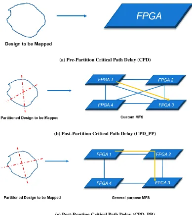
Critical Path Delay
In synchronous digital circuits, the speed of a mapped design is governed by the slowest
combinational path in the circuit implementation, which is called the critical path. There
are three different critical path delays: Pre-partition critical path delay (CPD),
26
Critical path delay of the un-partitioned LUT-level netlist is called CPD. It is calculated by
assuming that the complete design is mapped on a hypothetical single large FPGA and
there are no off-chip delays in the critical path as shown in Figure 3.1 (a).
CPD_PP is the critical path delay obtained by analyzing the circuit netlist after it has been
partitioned into multiple FPGAs. The circuit is annotated with the inter-FPGA delays. Here
it is assumed that the design is mapped on a custom MFS, which has no routing limitations
and it provides full connectivity as shown in Figure 3.1 (b). CPD_PP is calculated by
adding all the delays encountered when connecting a CLB in one FPGA to a CLB in
another FPGA. CPD_PP is the sum of the following three delay values: CLB-to-output pad
routing delay, PCB or optical trace delay and input pad-to-CLB routing delay.
Speed of an MFS is determined primarily by the latency bound i.e. the length of the
post-routing critical path (CPD_PR) obtained after a synchronous design has been placed and
routed at the inter-chip level [1]. CPD_PR is governed by the internal design delay, the I/O
pad delays and off-chip routing delays. As compared to the internal delay, board routing
delays exercise a larger impact on the overall system performance. The routing architecture
employed and the type of interconnections used mainly dictates the system routing delay.
CPD_PR is the same as CPD_PP but it also takes into account any route-throughs which
can occur due to MFS limited routing architectures as in TORUS. As shown in Figure 3.1
(c), in route-through scenario, the signal does not have a direct path from source to
destination FPGA and therefore, it has to traverse through an intermediate FPGA. When a
signal is sent from the source FPGA (FPGA 1), it enters into one pin of the intermediate
FPGA (FPGA 2), travels through the on-chip routing lines and then exits through the other
pin, without utilizing any of the on-chip logic of the intermediate FPGA. Then the signal
reaches its destination FPGA (FPGA 3). Detailed discussion on critical path delays and
27
(a) Pre-Partition Critical Path Delay (CPD)
(b) Post-Partition Critical Path Delay (CPD_PP)
(c) Post-Routing Critical Path Delay (CPD_PR)
Figure 3.1: Critical Path Delays
3.3.
Logic Multiplexing
Logic Multiplexing requires multiple compatible inter-FPGA signals to be assembled and
serialized through the same single-ended board trace and then de-multiplexed at the
destination FPGA. Using I/O flip-flops makes the timing of inter-FPGA connections more
predictable and generally faster in case of asynchronous multiplexing where system clock
and multiplexer/de-multiplexer clock are not phase aligned [21]. In this research, we have
28
Figure 3.2: Logic Multiplexing Scheme
The multiplexer/de-multiplexer clock and the system clock for the FPGAs are mutually
synchronous i.e., they are derived from one clock source, PLL (Phase Locked-Loop) and
are phase aligned.
As discussed earlier, CPD_PR determines the speed of a design in an MFS. In a
multi-FPGA board, CPD_PR is the sum of: source intra-multi-FPGA routing delay, output pad delay
(Tout), board trace delay (Ttrace), input pad delay (Tin) and destination intra-FPGA routing
delay as shown in Figure 3.2. In order to ensure synchronization between source and
destination FPGA clocks we add a safety margin of 20% to CPD_PR. Therefore, we can
obtain the delay on a multiplexed connection in Logic multiplexing scheme and mux_clk
can be written as (3.1).
𝑚𝑢𝑥_𝑐𝑙𝑘 = 1
1.20 ∗ 𝐶𝑃𝐷_𝑃𝑅 (𝑀𝐻𝑧) (3.1)
On the transmitter end, n-bit wide data from the internal domain is multiplexed by ω-bit
wide logic multiplexer which is inserted to accommodate the signals exceeding the
transmission capacity. ω is the multiplexing ratio and it represents the number of
29
Therefore, the relationship between sys_clk_lm and mux_clk in logic multiplexing scheme
for a given range of multiplexing ratio ω [5] can be calculated by (3.2):
𝑠𝑦𝑠_𝑐𝑙𝑘_𝑙𝑚 = 𝑚𝑢𝑥_𝑐𝑙𝑘
𝜔 (𝑀𝐻𝑧) (3.2)
3.4.
SERDES
As discussed earlier, high-speed FPGA interconnections are inevitable in present
technology. The traditional method of parallel transmission is becoming inadequate and is
replaced by serial data communication meeting higher bandwidth requirements. In serial
high speed I/O interfaces, instead of transmitting in parallel, the stream of serial data is
transmitted one bit per time on each link. All modern FPGAs are equipped with
serialization and deserialization (SERDES) modules which provide serial-to-parallel
conversions on incoming data and parallel-to-serial conversion on outgoing data. The
common approach employed to transmit data is single-ended signaling where one off-chip
trace is used to carry the transmitted signal as in logic multiplexing scheme. However, for
data rates exceeding gigabits per second (Gbps), differential signaling is preferred rather
than single-ended transmission. SERDES allow operation at speeds greater than 1Gbps per
line, using low-voltage differential signaling (LVDS) data transmission [29].
3.4.1. LVDS Signaling
LVDS is a fast, low-power, low-voltage and low-noise general-purpose input output (I/O)
interface standard which requires two pins for each serialized data stream.
ANSI/TIA/EIA-644 standard and IEEE Std. 1596.3 define physical layer (PHY) of LVDS. Typical
applications of LVDS include high-speed video, graphics, flat panel displays, general
purpose computer buses etc.
LVDS driver has a nominal 3.5 mA current source located in it as shown in Figure 3.3.
Since the input impedance of the receiver is high, the entire current flows through the 100Ω
terminating resistor resulting in a 350 mV voltage drop across the receiver inputs. LVDS
receiver threshold is certain to be 100 mV or less and this sensitivity is kept constant over
30
and tolerance to common-mode shifts between the driver and the receiver. Changing the
direction of current results in the same amplitude but opposite polarity at the receiver end.
350 mV typical signal swing consumes small amount of power and makes LVDS a very
power efficient technology.
Figure 3.3: LVDS Architecture
The main advantages of LVDS signaling are as follows:
• High data rates can be attained with low power consumption. • Better noise performance as compared to single-ended signaling.
• Low voltage swing as compared to other industry data transmission standards,
consequently LVDS achieves a high aggregate bandwidth in point-to-point
applications.
The main disadvantages of LVDS communication include:
• Skin effect, dielectric losses and reflections.
• Long parallel links are affected by signal integrity and skew.
In multi-FPGA setup, the OSERDES module in the transmitter FPGA translates the single
input signal into a pair of output signals which are driven 180° out of phase with each other
onto the PCB traces. The ISERDES module in the receiver FPGA recovers the signal as
the difference in the voltages on the two lines. The voltage difference between these two
signals defines the value of the resulting LVDS signal. External electromagnetic
interference (EMI) tends to affect both signals equally, however, since at the receiving end
![Figure 2.1: Hard-wired MFS (DNV7F4A) [2]](https://thumb-us.123doks.com/thumbv2/123dok_us/1372895.1170008/27.612.114.520.121.394/figure-hard-wired-mfs-dnv-f-a.webp)
![Figure 2.2: Photograph of 2 TwinStar FPGA Systems [14]](https://thumb-us.123doks.com/thumbv2/123dok_us/1372895.1170008/28.612.202.449.247.478/figure-photograph-of-twinstar-fpga-systems.webp)
![Figure 3.9: NoC Emulation Board [34]](https://thumb-us.123doks.com/thumbv2/123dok_us/1372895.1170008/62.612.165.490.402.692/figure-noc-emulation-board.webp)
![Figure 4.1: Optical Interface Evolution [39]](https://thumb-us.123doks.com/thumbv2/123dok_us/1372895.1170008/67.612.112.528.73.343/figure-optical-interface-evolution.webp)
