Available online: https://edupediapublications.org/journals/index.php/IJR/ P a g e | 233
Design and Verification of High Speed and Energy Efficient Carry Skip
Adder
Dasari Siva Kumari, PG Scholar, Dept. Of ECE,
Email-Id:
[email protected]
Mrs. Yarram Uma Maheswari, M.Tech [Associate Professor Dept. Of ECE],
Email-Id:
[email protected]
Sannikanti Kishore Babu, M.Tech, [Ph.D] [Associate Professor &
HOD Dept. Of ECE], Email-Id:
[email protected]
Vikas Group Of Institutions, Nunna(V) , Vijayawada(M) - 521 212, Krishna Dts.
ABSTRACT :
In this paper, we present a carry skip adder (CSKA) structure that has a higher speed yet lower energy consumption compared with the conventional one. The speed enhancement is achieved by applying concatenation and incrementation schemes to improve the efficiency of the conventional CSKA (Conv-CSKA) structure. In addition, instead of utilizing multiplexer logic, the proposed structure makes use of AND-OR-Invert (AOI) and OR-AND-Invert (OAI) compound gates for the skip logic. As the number of transistors is reduced to half by using AOI/OAI logic when compare to MUX, Power reduction is achieved without compromising the speed making it suitable for
wide range of low-power applications. The
structure may be realized with both fixed stage size and variable stage size styles, wherein the latter further improves the speed and energy parameters of the adder. The hybrid variable latency structure, which lowers the power consumption without considerably impacting the speed, is presented. This extension utilizes a modified parallel structure for increasing the slack time, and hence, enabling further voltage reduction. The proposed structures are assessed by comparing their speed, power, and energy parameters with those of other adders using a 45-nm static CMOS technology for a wide range of supply voltages. In addition, the power–delay product was the lowest among the structures
considered in this paper, while its energy–delay product was almost the same as that of the Kogge–
Stone parallel prefix adder with considerably smaller area and power consumption.
Keyword's:- Carry Skip Adder(CSKA), Concatenation and Incrementation CSKA, AND-OR-Invert (AOI) and OR-AND-Invert (OAI).
I. INTRODUCTION
Adders are the key building block in arithmetic and logic units (ALU s) [1] and hence increasing their speed and reducing their power/energy consumption strongly affect the speed and power consumption of processors. There are many works on the subject of optimizing the speed and power of these units, which have been reported in [2]–[9]. Obviously, it is highly desirable to achieve higher speeds at low- power/
energy consumptions, which is a challenge for the designers of general purpose processors.
Available online: https://edupediapublications.org/journals/index.php/IJR/ P a g e | 234 significantly lowers switching and leakage
powers compared with the super threshold region.
Achieving higher speeds at lower supply voltages for the computational blocks, with the adder as one the main components, could be crucial in the design of high-speed, yet energy efficient, processors. There are many adder families with different delays, power consumptions, and area usages. Examples include ripple carry adder (RCA), carry increment adder (CIA), carry skip adder (CSKA)
[4]
, carry select adder (CSLA)[5]
, and parallel prefix adders (PPAs). The descriptions of each of these adder architectures along with their characteristics may be found in [1] and [7]. The RCA has the simplest structure with the smallest area and power consumption but with the worst critical path delay. In the CSLA, the speed, power consumption, and area usages are considerably larger than those of the RCA. The PPAs, which are also called carry look-ahead adders, exploit direct parallel prefix structures to generate the carry as fast as possible [8].The critical path delay of the CSKA is much smaller than the one in the RCA, whereas its area and power consumption are similar to those of the RCA. In addition, the power-delay product (PDP) of the CSKA is smaller than those of the CSLA and PPA structures.
In this paper, given the attractive features of the CSKA structure, we have focused on reducing its delay by modifying its implementation based on the static CMOS logic.
II. LITERATURE WORK
The focus of this paper is on the CSKA structure, first the related work to this adder are reviewed and then the carry skip adder structure for CI-CSKA are discussed.
A. Modifying CSKA for Improving Speed The conventional structure of the CSKA consists of stages containing chain of full adders (FAs) (RCA block) and 2:1 multiplexer (carry skip logic). The RCA blocks are connected to each other through 2:1 multiplexers, which can be placed into one or more level structures [10]. The CSKA configuration (i.e., the number of the FAs
per stage) has a great impact on the speed of this type of adder [8]. Many methods have been suggested for finding the optimum number of the FAs. Some methods to increase the speed of the multilevel CSKAs are proposed. The techniques, however, cause area and power increase considerably and less regular layout. The design of a static CMOS CSKA where the stages of the CSKA have a variable sizes was suggested in [8]. In addition, to lower the propagation delay of the adder, in each stage, the carry look-ahead logics were utilized.
B. Improving Efficiency of Adders at Low Supply Voltages
The voltage reduction must not increase the delays of the noncritical timing paths to become larger than the period of the clock allowing us to keep the original clock frequency at a reduced supply voltage level. When the critical timing paths in the adder are activated, the structure uses two clock cycles to complete the operation. This way the power consumption reduces considerably at the cost of rather small throughput degradation.
III. CONVENTIONAL CARRY SKIP ADDER
The structure of an N-bit Conv-CSKA, which is based on blocks of the RCA (RCA blocks), is shown in Fig. 1. In addition to the chain of FAs in each stage, there is a carry skip logic. the worst case delay belongs to the case
Pi = Ai ^ Bi = 1 for i = 1,…..N.
Available online: https://edupediapublications.org/journals/index.php/IJR/ P a g e | 235 where Pi is the propagation signal
related to Ai and Bi. In the CSKA, the carry
skip logic detects this situation, and makes the carry ready for the next stage without waiting for the operation of the FA chain to be completed. The skip operation is performed using the gates and the multiplexer shown in the figure. the product of the propagation signals (P) of the stage is used as the selector signal of the multiplexer. The CSKA may be implemented using FSS and VSS where the highest speed may be obtained for the VSS structure.
Fig 1: Conventional Structure of the CSKA.
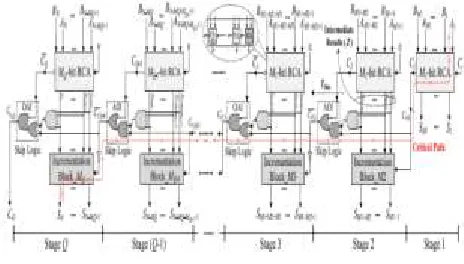
IV. PROPOSED CSKA STRUCTURE
A. Description of the Proposed Structure The structure is based on combining the concatenation and the incrementation schemes with the Conv-CSKA structure, and hence, is denoted by CI-CSKA. It provides us with the ability to use simpler carry skip logics. The logic replaces 2:1 multiplexers by AOI/OAI compound gates (Fig. 2). The gates, which consist of fewer transistors, have lower delay, area, and smaller power consumption compared with those of the 2:1 multiplexer. in this structure, as the carry propagates through the skip logics, it becomes complemented. Therefore, at the output of the skip logic of even stages, the complement of the carry is generated. The structure has a considerable lower propagation delay with a slightly smaller area compared with those of the conventional one. Note that while the power consumptions of the AOI (or OAI) gate are smaller than that of the
multiplexer, the power consumption of the proposed CI-CSKA is a little more than that of the conventional one. This is due to the increase in the number of the gates, which imposes a higher wiring capacitance (in the noncritical paths).
The stages 2 to Q consist of two blocks of RCA and incrementation. The incrementation block uses the intermediate results generated by the RCA block and the carry output of the previous stage to calculate the final summation of the stage. The internal structure of the incrementation block, which contains a chain of half-adders (HAs), is shown in Fig. 3. In addition, note that, to reduce the delay considerably, for computing the carry output of the stage, the carry output of the incrementation block is not used.
Fig 2 : Proposed Structure For CI-CSKA
Available online: https://edupediapublications.org/journals/index.php/IJR/ P a g e | 236 The reason for using both AOI and OAI
compound gates as the skip logics is the inverting functions of these gates in standard cell libraries. This way the need for an inverter gate, which increases the power consumption and delay, is eliminated. As shown in Fig. 2, if an AOI is used as the skip logic, the next skip logic should use OAI gate. In addition, another point to mention is that the use of the proposed skipping structure in the Conv-CSKA structure increases the delay of the critical path considerably. This originates from the fact that, in the Conv-CSKA, the skip logic (AOI or OAI compound gates) is not able to bypass the zero carry input until the zero carry input propagates from the corresponding RCA block.
B. Area and Delay of the Proposed Structure The use of the static AOI and OAI gates (six transistors) compared with the static 2:1 multiplexer (12 transistors), leads to decreases in the area usage and delay of the skip logic. In addition, except for the first RCA block, the carry input for all other blocks is zero, and
hence, for these blocks, the first adder cell in the RCA chain is a HA. This means that (Q − 1) FAs in the conventional structure are replaced with the same number of HAs in the suggested structure decreasing the area usage (Fig. 2). In addition, note that the proposed structure utilizes incrementation blocks that do not exist in the conventional one. These blocks, however, may be implemented with about the same logic gates (XOR and AND gates) as those used for generating the select signal of the multiplexer in the conventional structure.
The comparison of CSKA and CI-CSKA structures indicates that the delay of the proposed structure is smaller than that of the conventional one. The First reason is that the delay of the skip logic is considerably smaller than that of the conventional structure while the number of the stages is about the same in both structures. Second, since TAND and TXOR are
smaller than TCARRY and TSUM, the third additive term becomes smaller than the third term.
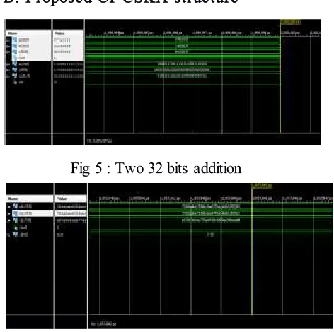
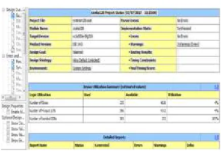
V. SIMULATION RESULTS Simulated the existing and proposed system structures in Isim simulator. These results are developed for the Spartan 3E FPGA Family kit[6] by using Xilinx (14.5) software [3]. The simulation results for Existing 32bit CSKA, Proposed 32 bit CI-CSKA, Proposed system extension of 128 bit CI-CSKA and its Design summary are shown in the below Fig 4, 5, 6 & 7.
A. Conventional CSKA structure
Fig 4 : Two 32 bits addition
B. Proposed CI-CSKA structure
Fig 5 : Two 32 bits addition
Available online: https://edupediapublications.org/journals/index.php/IJR/ P a g e | 237 C. Design summary
Fig 6 : Design summary of Two 128 bits using CI-CSKA
VI. CONCLUSION
In this paper, a static CMOS CSKA structure called CI-CSKA was proposed, which exhibits a higher speed and lower energy consumption compared with those of the conventional CSKA. The speed enhancement was achieved by modifying the structure through the concatenation and incrementation techniques. In addition, AOI and OAI compound gates were exploited for the carry skip logics. The efficiency of the proposed structure for both FSS and VSS was studied by comparing its power and delay with those of the Conv-CSKA, RCA, CIA, SQRT-CSLA, and CSKA structures. The results revealed considerably lower PDP for the VSS implementation of the CI-CSKA structure over a wide range of voltage from super-threshold to near threshold. The results also suggested the CI-CSKA structure as a very good adder for the applications where both the speed and energy consumption are critical.
VII.REFERENCES
[1] I. Koren, Computer Arithmetic Algorithms, 2nd ed. Natick, MA, USA: A K Peters, Ltd.,
2002.
[2] R. Zlatanovici, S. Kao, and B. Nikolic, “Energy–delay optimization of 64-bit carry-lookahead adders with a 240 ps 90 nm CMOS design example,” IEEE J. Solid-State Circuits, vol. 44, no. 2, pp. 569–583, Feb. 2009.
[3]. Xilinx Design Tools: Installation and
Licensing Guide (UG798):
http://www.xilinx.com/support/documentation/s w_manuals/xilinx14_1/iil.pdf
http://www.xilinx.com/support/documentati
on/sw_manuals/xilinx14_1/ug682.pdf
[4]. S. Majerski, “On determination of optimal distributions of carry skips in adders,” IEEETrans. Electron. Comput., vol. EC-16, no. 1, pp. 45–58, Feb. 1967.
[5]. B. Ramkumar and H. M. Kittur, “Low-power and area-efficient carry select adder,” IEEE Trans. Very Large Scale Integr. (VLSI) Syst., vol. 20, no. 2, pp. 371–375, Feb. 2012. [6].Gone through the Spartan-3E FPGA Family Data Sheet
[7] C. Nagendra, M. J. Irwin, and R. M. Owens, “Area-time-power tradeoffs in parallel adders,” IEEE Trans. Circuits Syst. II, Analog Digit. Signal Process., vol. 43, no. 10, pp. 689–702, Oct. 1996.
[8] Y. He and C.-H. Chang, “A power-delay efficient hybrid carrylookahead/ carry-select based redundant binary to two’s complement converter,” IEEE Trans. Circuits Syst. I, Reg. Papers, vol. 55, no. 1, pp. 336–346, Feb. 2008. [9] C.-H. Chang, J. Gu, and M. Zhang, “A review of 0.18 μm full adder performances for tree structured arithmetic circuits,” IEEE Trans. Very Large Scale Integr. (VLSI) Syst., vol. 13, no. 6, pp. 686–695, Jun. 2005.