Subthreshold Circuit Design Techniques for
Ultra Low-Power Applications
K.A.Jyotsna1, P.Satish Kumar2, B.K.Madhavi3
Associate Professor, Dept. of ECE, CVR College of Engineering, Hyderabad, Telangana, India1
Professor, Dept. of ECE, ACE Engineering College, Hyderabad, Telangana, India2
Professor, Dept. of ECE, Sreedevi Women’s Engineering College, Hyderabad, Telangana, India3
ABSTRACT: This paper presents novel approach called sub threshold source coupled logic (STSCL) used for low voltage and low power applications . This Logic provides a promising performance with excellent energy savings. Basic logic gates are designed and analysed using STSCL and sub threshold CMOS in 45nm technology at different power supplies using cadence virtuoso tools .As the circuits work in sub threshold region they can be operated in a wide frequency range by adjusting the tail bias current to as low as 1n A thereby offering a great increase in their power delay product.
KEYWORDS: Sub threshold Source Coupled Logic, Differential logic, Complementary MOS, Binary decision diagrams.
I. INTRODUCTION
The need for low power and high speed designs have increased in the past decade. This demand is achieved by making the circuits work in the sub threshold region which is possible by making the power supply VDD less than the threshold voltage Vth of the MOS transistor.
Sub threshold operation leads to the achievement of ultra low power consumption with the devices working from hundred to few mega hertz frequency and can be used in applications like medical equipments such as hearing aids, pace-makers, implants, energy scavenging applications and laptops as well as high-performance parallel processing.
A good alternative for Sub threshold CMOS circuits are Sub threshold Source Coupled logic (STSCL) circuits which can also be used for mixed signal applications. These STSCL circuits have become popular for low power, high performance applications. STSCL circuits work in differential logic so they have less switching noise, common mode noise, less sensitivity to supply, process and temperature variations. [1]
STSCL circuits have more advantages when compared to CMOS and can be used in applications where ultra low power dissipation is needed .One of the biggest advantages of STSCL Circuits is its tail bias current which can be lowered to few pico amperes which is less than the leakage current of the conventional CMOS devices.
II. SUB THRESHOLD LOGIC FAMILIES
A. SUBTHRESHOLD CMOS LOGIC
In the past decade Conventional CMOS technology has been used to implement high performance digital circuits which has less area and negligible static power consumption. For more complex digital systems CMOS technology has been continuously scaled down which lead to some adverse secondary effects like increase in the device leakage current, increase in the static power and hence decreased power efficiency.
B. SUBTHRESHOLD SOURCE COUPLED LOGIC
STSCL circuits work in sub threshold region that is their supply voltage VDD is less than the threshold Voltage Vth . This paper presents a new STSCL logic families which work in current domain with differential logic principle with the circuit consisting of differential inputs and differential outputs [6]. The entire operation of the circuit depends on the tail bias current ISS. For STSCL circuit the power dissipation ,delay and threshold voltage does not depend on the supply voltage thereby relaxing the tight tradeoffs among these parameters.[8]
In STSCL circuit, NMOS Differential pair is the main part of the circuit which implements the logic operation of the circuit. The basic STSCL Inverter is shown below in figure 1 which consist of two NMOS transistors M3 and M4 which act as the differential pair with two inputs Vin and Vinb. As resistors occupy more area, hence PMOS Transistors M1 and M2 act as load with their bulk and drain connected [3].They provide high resistance so that very less tail bias current ISS is obtained. This tail bias current is obtained by the NMOS transistor M5.
The tail bias current ISS is directed to one of the two load transistors M1 and M2 and the output signal is obtained by these two PMOS transistors is converted into differential output voltage Vout and Voutb.[4]
Fig.1 STSCL Inverter Circuit
In STSCL Circuits, very low power dissipation and less delay are obtained which is given by the equations 1,2.3 below
Power Dissipation = VDD × ISS --- (1)
The output voltage swing Vswing of STSCL is decided by the tail bias current ISS and the resistive load RL.
Vswing= RL × ISS --- (2)
The Time delay of STSCL is given by
τ
SCL = RL × CL = VSW / ISS × CL --- (3)The above equations indicate that the entire STSCL operation depend on the tail bias current ISS
III. DESIGN AND SIMULATION
Fig 2 Binary Decision Diagram of STSCL AND/NAND Gate and its truth table
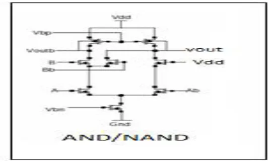
In the binary decision diagram of two input AND gate as shown in figure 2 Above , the nodes 0 and 1 show both the complementary outputs of the STSCL gates. With the help of the binary decision diagrams, the other STSCL basic gates are obtained as shown in the figures 3 and 4 [2].
Fig 4 STSCL XOR/XNOR Gates, OR/NOR Gates
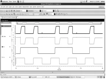
All the circuits are designed using Cadence Virtuoso tools and all the logic gates are simulated using 45nm technology and the simulated output waveforms of STSCL AND/NAND gates are shown in the figure 5 below [5]. With a two inputs and the differential outputs as AND output and NAND output.
The simulated output waveforms of STSCL OR/NOR gates are shown in the figure 6 below, with two inputs a and b and two differential outputs as OR output and NOR output
Fig 6 Output of STSCL OR/NOR gates
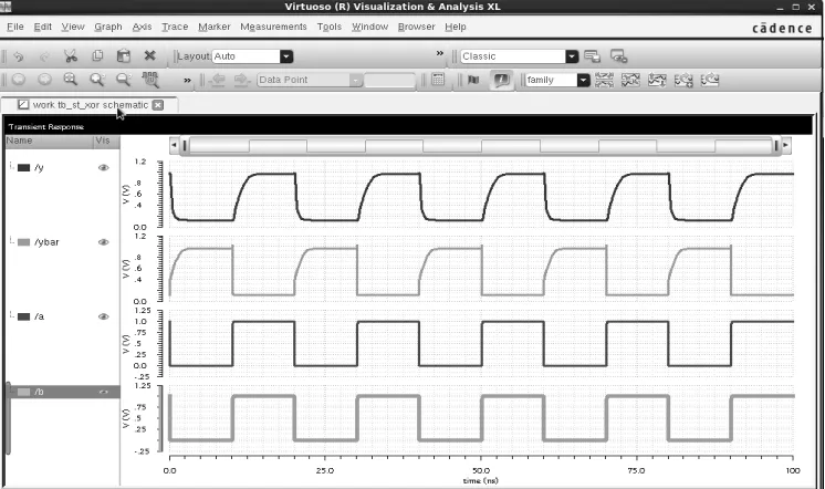
The simulated output waveforms of STSCL XOR/NOR gates are shown in the figure 7 below, with two inputs a and b and two differential outputs as XOR output and XNOR output
IV. MEASURED RESULTS
Different STSCL Logic gates are designed and verified in 45 nm technology. Their power and delay are calculated and compared with CMOS basic gates which is given below in the tabular form 1 at power supply of 1V [10] .
TABLE 1
POWER AND DELAY OF BASIC GATES IN 45NM TECHNOLOGY FOR STRONG INVERSION REGION AT VDD =1V
Basic Gates
CMOS STSCL
Power(W) Delay(sec) Power(W) Delay(sec)
Inverter 5E-3 30.4E-6 7.28E-6 25.32E-12
OR 16.69E-9 20.24E-9 18.76E-6 19.88E-12
AND 10.92E-9 20.16E-9 22.96E-6 10.04E-12
NOR 7.26E-9 84.12E-12 18.76E-6 10.1E-9
NAND 7.51E-9 39.54E-12 22.9E-6 28.33E-12
Sub threshold source coupled logic works in sub threshold region so the condition to be satisfied is that the power supply of the circuit should be less than the threshold voltages of NMOS and PMOS transistors. The threshold voltage of NMOS Transistor is found to be 0.592V for NMOS Transistor and for the PMOS transistor it is -0.482V in 45nm Technology. Hence in the table 2 below the power and delay of all the basic gates in CMOS and STSCL logic with a power supply of 0.5V is measured and compared in sub threshold region [7].
TABLE 2
POWER AND DELAY OF BASIC GATES IN 45NM TECHNOLOGY FOR SUBTHRESHOLD REGION AT VDD = 0.5V
Basic Gates
CMOS STSCL
Power(W) Delay(sec) Power(W) Delay(sec)
Inverter 201E-12 11.41E-9 100.1E-12 2.73E-9
OR 351.5E-12 20.24E-6 7.54E-9 28.64E-6
AND 38.26E-12 20.21E-6 1.26E-9 39.23E-6
NOR 339.9E-12 6.43E-9 7.54E-9 17.48E-6
NAND 37.3E-12 32.28E-9 1.26E-9 10.09E-9
V. CONCLUSION
A novel technique for implementing ultra low power STSCL circuits is presented in this paper. The proposed approach benefits from less area , more speed and ultra low power operation . Here an analytical approach for studying and comparing the performance and power of ultra-low power CMOS and STSCL circuit, has been presented. While there is a tight tradeoff among power consumption, speed of operation, and supply voltage in design of CMOS digital circuits [11], STSCL topology provides a more convenient design opportunity for ultra-low power applications.
REFERENCES
[1] S. A. Tajalli, E. J. Braurer, Y. Leblebici, E. Vittoz, "Sub threshold Source-Coupled Logic Circuits for Ultra-Low-Power Applications," IEEE Journal of Solid-State Circuits, vol. 43, no. 7, pp. 1699-1710, July 2008.
[2] Mohd Beikahmadi “ Developing a standard cell library for STSCL” Master thesis, Ecole Polytechnique Federale de Lausanne (EPFL), Switzerland, 2009.
[3] S. A. Tajalli, E. Vittoz, E. J. Braurer, Y. Leblebici, "Ultra-low power sub threshold current- mode logic utilizing PMOS load device" Electronics Letters ,vol. 43, no. 17, August 2007.
[4] S. A. Tajalli,,Y. Leblebici, "Leakage current Reduction using Sub threshold Source Coupled Logic” IEEE Transactions on circuits and systems-2: Express Briefs, Vol 56,No 5, May 2007.
[5] S. Badel “ MOS Current-Mode logic standard cells for high-speed low noise applications,” PhD Dissertation, Ecole Polytechnique Federale de Lausanne (EPFL), Switzerland, 2008
[6] Sajib Roy,Md Myrad Kabir Nipun “Understanding Sub threshold Source coupled logic for ultra low power applications”, Master thesis ,Linkoping Univrsity,Sweden,2011.
[7] K.Ragini, DR B.K.Madhavi “Ultra low power digital logic circuits in sub threshold for biomedical applications”pp 544-590,Journal of theoretical and applied information technology,August,2009.
[8] A. Tajalli and Y. Leblebici, “Design tradeoffs in ultra-low-power digital nano-scale CMOS,” in IEEE Transactions. on Circuits. and Systems.-I, 2011.
[9] Ashutosh Nandi, Gaurav Saini, Amit Kumar Jaiswal, & Kamal Kant “Robust Sub threshold Circuit Designing Using Sub-threshold Source Coupled Logic (STSCL) ’’ International Journal of Electronics Engineering, Vol 2, pp. 219-223,2010.
[10] Sumit Vyas, and Sanjeev Rai, “A Survey on Power-Delay Reduction Techniques for Ultra-Low-Power Sub threshold SCL Circuits” IEEE Journal Of Solid-State Circuits, Vol. 33, No. 7, July 2009
[11] A. P. Chandrakasan, S. Sheng, R. W. Brodersen,“Low- power CMOS digital design,” IEEE J. Solid-State Circuits, Vol. 27, pp. 473– 484, Apr. 1992.