Generalized PWM Algorithm for 3-level
Diode Clamped Inverter fed Direct Torque
Controlled Induction Motor Drive
Dr.J.Bhavani
1, Dr.D.Subba Rayudu
2Senior Assistant Professor, Dept. of EEE, VNRVJIET, Hyderabad, A.P, India1
Director & Professor, Sri Srinivasa Co llege of Engg.& Technology, Kurnool, A.P, India2
ABSTRACT
:
This paper presents a simp le generalized pulse width modulation (GPWM) algorith m for three-level diodecla mped inverter fed direct torque controlled induction motor drives. Though the classical direct torque control (DTC) algorith m gives fast dynamic response, it gives large steady state ripples and variable switching frequency operation of the inverter. To overco me these problems, space vector pulse width modulation (SVPWM) algorithm is used for DTC drives. In order to meet the require ments of high power applicat ions, nowadays multilevel inverter fed drives are becoming popular. But, the co mple xity involved in the classical SVPWM algorith m based three-level inverter is more. Hence, to reduce the comple xity involved, the proposed algorithm uses the instantaneous phase voltages only. Moreover, the proposed approach gives the realizat ion of various carrier based PWM algorith ms tha t include both SVPWM and various discontinuous PWM (DPWM) a lgorith ms by using a generalized control algorithm and is obtained via unequal sharing of
zero states. In the proposed approach, by varying a constant k value from ze ro to one, various DPWM algorithms can
be generated along with the SVPWM algorith m. To validate the proposed GPWM algorithm based DTC drive, several numerical simu lation studies have been carried out and the results have been presented. The simu lation results show the effectiveness of the proposed algorithm.
KEYWORDS: DPWM, DTC, GPWM, Induction motor drive, SVPWM, three-level inverter.
1.INTRODUCTION
The variable speed drives (VSDs) are becoming popular in many industrial applications. The invention of fie ld oriented control (FOC) a lgorith m has been made a renaissance in the high -performance variable speed drive applications. The FOC algorith m gives the decoupling control of torque and flux of an induction motor drive and control the induction motor similar to a separately e xcited dc motor [1]. But, the co mple xity involved in the FOC a lgorith m is more due to reference fra me transformations. To reduce the comple xity involved, a new control strategy called as direct torque control (DTC) has been proposed in [2]. A detailed comparison between FOC and DTC is presented in [3] and concluded that DTC gives fast torque response when compared with the FOC. Though, FOC and DTC g ive fast transient and decoupled control, these operate the inverter at variab le switching frequency due to hysteresis controllers. Moreover, the steady state ripples in torque, flu x and currents are high in DTC.
(SVPWM) has become one of the most popular PWM methods for three -phase inverters [5]. It uses the SV approach to compute the duty cycle of the switches. The main features of this PWM algorith m are easy digital imple mentation and wide linear modulation range for output line-to-line voltages. Though, the SVPWM gives superior performance, it gives more switching losses of the inverter as it has continuous modulating signal. Hence, to reduce the switching losses of the inverter, nowadays discontinuous PWM (DPWM) algorith ms are becoming popular. The generation of these DPWM algorith ms is given in detail in [6]-[10].
The two-level voltage source inverters are not suitable for med iu m and high power applications due to large dv/dt stresses and more harmonic distortion. In order to reduce these problems three -level inverters are introduced in 1980s [11]. The detailed survey on mult ileve l inverter topologies is given in [12]. In order to obtain controllable three phase power fro m a mu ltilevel inverter, various PWM algorith ms can be generated by using both SV and TC approaches. However, in SV approach the comple xity will be increased due to the more number of voltage vectors. Hence, in most number of applications the carrier based PWM algorithms are popular for mult ileve l inverters. Few simp lified approaches by using duty cycle and offset times have been proposed for carrier based SVPWM algorith m based multilevel inverters [13], [14].
This paper presents carrier based generalized PWM (GPWM) algorith m fo r 3 -level inverter fed direct torque controlled induction motor drives. In the proposed GPWM algorithm by changing a constant value between 0 and 1, various PWM algorithms have been generated. Moreover, the proposed algorithm uses instantaneous phase voltages only. Thus, the proposed GPWM a lgorith m will bring all modulators under a common roof with reduced comple xity.
II.THREE L EVEL DIODE CLAMPED INVERTER
The three-level diode cla mped inverter is also known as neutral point clamped (NPC) inverter. The NPC configuration
was first proposed by Nabae, et.al in 1981. Fig. 1 shows the power circu it of a 3-phase, three-level NPC inverter. Node 'o'
indicates the negative bus and 'm' is the midpoint of the dc bus. Switches ( Sa1,Sa2 ) of phase a, ( Sb1,Sb2 ) of
phase b and ( Sc1,Sc2 ) of phase c are the main devices operating as modulating switches for the PWM. Sa2,Sa1,Sb2
,Sb1, Sc2and Sc1 are the auxilia ry switches to cla mp the output voltage to the midpoint together with the diodes Da1, Da2,
Db1, Db2, Dc1, and Dc2.
Assume the dc rail o is the reference point of the output phase voltage. For an output voltage level 2 , turn on all
upper-half switches Sa1Sa2. For an output voltage level Vao0,turn on the middle switches Sa1 and Sa2 . For an output voltage
level VaoVdc 2 , turn on the lower ha lf switches Sa1 and Sa2 .
p
S
a1S
b1S
c1V
dcC
D
a1D b1
D
c1 2m
S a2 S b2 S c2IM
S
S
S
a1 b1 c1 D b2 V dc
C
D a2 D c2 2S
S S a2 b2 c2
o
Fig. 1 Topology of 3-phase, 3-level diode cla mped inverter
III. PROPOS ED GPWM ALGORITHM
The proposed GPWM a lgorith m may be pursued by the definition of a duty cycle or modulat ing signal for phase n (with
n = a, b and c), which is given as the ratio between pulsewidth and modulation period.
V
*
Pulsewidth
(1)
n
Modualtionperiod
Once the modulat ing signal Vn* is calculated, the ON and OFF times of the inverter-leg devices can be via dig ital
counters and comparators. For e xa mp le, the duty cycle or modulating signal of SPWM algorithm can be obtained as follows [9]-[10].
Where Vn is the instantaneous reference
voltage of phase n and Vdc is the dc-link voltage. In the similar way, the modulating signals of the various DPWM
algorith ms and SVPWM algorith ms can be obtained by adding a suitable zero sequence voltage (Vz ) to the instantaneous
phase voltages (Vz).
.
V
*
k
V
n
V
z(3)
n n 1
V
dc *
1
V
n,
n
a
, b and c
(2)
V
n
where Vz k2[min( Vn ) ma x( Vn )] min(Vn ) (4)
where k2 is the parameter that takes into account the unequal null-state sharing, can be defined as follows:
k
2
0.5(1
sgn(cos(3
t
))
(5)
where sgn(X) is 1, 0 and –1 when X is positive, zero, and negative, respectively. As previously discussed, and k1 is an
additional parameter whose value may be equal to the value of k 2 or be fixed at 0.5. Thus, the proposed approach
eliminates the calculation of both the hexagon sector, in which the reference-voltage space vector is located, and the related phase.
In all the other carrier-based techniques, it must be taken that k1k2 . The standard SVPWM algorith m can be obtained
by fixing the k2 value at 0.5. Similarly, by fixing the k2 value at 0 and 1, the DPWMMIN and DPWMMAX algorith ms can
be obtained. By varying the modulation angle in (5), various DPWM algorith ms can be generated. The DPWM0,
DPWM1, DPWM2 and DPWM3 can be obtained for δ = π/6, 0, - π/6 and - π/3 respectively.
In conclusion, it is worth noticing that a mathemat ical e xp ression of the modulating signal in SVPWM was, in effect, already known, but it was referred only to classical SVPWM operating in linear modulation range. Here , the use of the modulating signal in the synthesis of the switching pattern has been put in evidence, and as a novelty, it has been extended
to the over modulation range and in generalized modulation by defining the new k1and k 2parameters.
After the generation of the modulating waves of various PWM algorithms, two triangular carrier signals have been generated in-phase as shown in Fig. 2. Then the modulating waves and carrie r waves have been compared and the switching signals have been generated as shown in Table-1.
Table-1: Generation of switching logic of the devices
Conditi on Switc h Status State
v
r
>
vt1and
v
r Sa
1
ON , Sa2 ON Sa
1> v
t 2 Sa1 OFF , S a2 OFF
v
r
<
vt1and
vr
>
vt 2 Sa
1
OFF,
Sa2ON Sa
0
ON
,
OFF
S
a1S
a2v
r
<
vt1and
vr
<
vt 2 Sa
1
OFF,
Sa
2
OFF Sa
1S
ON
,
S ONa1 a2
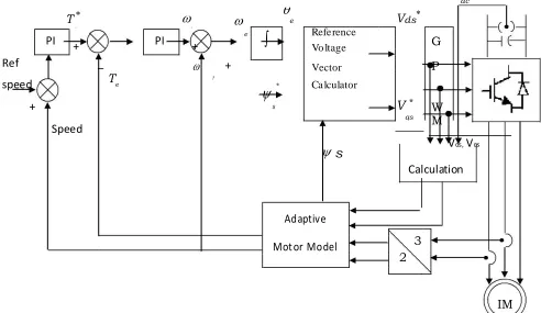
The block diagram of the proposed GPWM based DTC is as shown in Fig. 3. Fro m Fig. 3, it is seen that the proposed GPWM based DTC scheme retains all the advantages of the DTC, such as no co -ordinate transformation, robust to motor parameters, etc. However a space vector modulator is used to generate the pulses for the inverter, therefore the comple xity is increased in co mparison with the DTC method.
IV.PROPOS ED GPWM ALGORITHM B AS ED DTC
In the proposed method, the position of the reference stator flu x vect or s* is derived by the addition of slip speed and
actual rotor speed. The actual synchronous speed of the stator flu x vector s is calculated from the adaptive motor
model.After each sampling interval, actual stator flux vector s is corrected by the error and it tries to attain the reference
flu x space vectors* . Thus the flu x e rror is minimized in each sa mpling interval. The d -a xis and q-a xis co mponents of the
reference voltage vector can be obtained as follo ws:
Refe rence values of the d-a xis and q- a xis stator flu xes and actual values of the d-a xis and q-a xis stator flu xes are co mpared in the reference voltage vector calculator block and hence the errors in the d -axis and q-axis stator flux vectors are obtained as in (6)-(7).
ds
d s*
ds
(6)
qs
qs*
qs(7)
The appropriate reference voltage space vectors due to flu x erro r and stator ohmic drop are given as
v
* R i
ds(8)
ds ds s
T
sv
* R i
q s(9)
qs
qs s
T
sWhere, Ts is the duration of sub cycle or sampling period and it is a half of period of the switching frequency. This implies
vector are fed to the SVPWM b lock fro m wh ich, the actual switching times fo r each inverter leg are calcu lated.
dc
T
eV
dse sl
Refe rence
PI
+
PI
+
e
Vo ltageG
Ref
_
+
VectorP
speed
T
e r * Ca lculator+
sV
*W
qs
M
Speed
s
V
ds,V
qsCalculation
Adaptive
Mot or Model
3
2
IM
Fig.3 Block d iagra m of proposed SVPWM based DTC
V.S IMULATION RES ULTS AND DISCUSS ION
To validate the proposed generalized PWM algorithm based 3-level inverter fed DTC, several numerical simu lation studies have been carried out and results are presented. The details of the induction motor, which is used for simulatio n studies are as follows:
A 3-phase, 4 pole, 4kW, 1440 rp m induction motor with para meters as follows:
Rs = 1.57Ω, Rr = 1.21Ω, Ls = Lr = 0.17H, Lm = 0.165H and J = 0.089Kg.m2.
The steady state simu lation results for various PWM algorithms based 3-level inverter fed DTC drive are shown from Fig. 4 to Fig. 10. Fro m the simulat ion results, it can be observed that as the SVPWM algorith m is a continuous PWM algorith m, it gives continuous pulse pattern and more switching losses. Whereas, the DPWM algorithms cla mp each phase to either positive or negative DC bus for 120 degrees over a fundamental cycle, these reduce the switching frequency and switching losses by 33.33% when co mpared with the SVPWM a lgorith m. Thus, the proposed GPWM algorith m generates a
wide range ofPWM algorithms at a ll modulation indices with reduced comp le xity by varying a para meter k2
(a)
(b
)
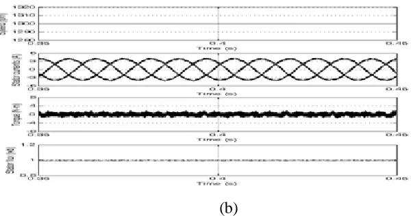
Fig. 4 Simulat ion results for SVPWM based DTC d rive
The Results given in fig.4(a) & (b ) are showing the Simu lation results of speed, currents, torque ,flu x for 3 level VSI fed SVPWM based DTC-IM drive and in fig.(b),the line current spectra with THD of 4.76% is shown .
(b)
Fig. 5 Simulat ion results for DPWMMIN based DTC drive
The Results given in fig.5(a ) showing the line current spectra with THD of 5.13 % and in fig.(b ) ,Simu lat ion results of speed, currents, torque ,flu x for 3 level VSI fed DPWMMIN based DTC-IM drive are shown .
(a)
(b)
Fig. 6.Simulat ion results for DPWMMAX based DTC drive
(a)
(b)
Fig.7. Simulat ion results for DPWM 0 based DTC drive
(a)
(b)
Fig.8 Simu lation results for DPWM1 based DTC drive
(a)
(b)
Fig.9 Simu lation results for DPWM2 based DTC drive
(a)
(b)
Fig.10. Simu lation results for DPWM3 based DTC drive
The Results given in fig.10(a ) showing the line current spectra with THD of 5.17% and in fig.(b) ,Simu lation results of speed, currents, torque ,flu x for 3 level VSI fed DPWM3 based DTC-IM drive a re shown.
VI. CONCLUS ION
A simp le and novel GPWM a lgorith m fo r three leve l inverter fed direct torque controlled induction motor drives is presented in this paper. The proposed algorithm generates a wide range of DPWM a lgorith ms along with SVPWM algorith m by using the instantaneous phase voltages only. Fro m the simulat ion results it can be observed that the proposed
REFERENCES
[1] F. Blaschke “The principle of field orientation as applied to the new transvector closed loop control system for rotating- field machines," Siemens
Review, 1972, pp 217-220.
[2] Isao Takahashi and Toshihiko Noguchi, “A new quick-response and high-efficiency control strategy of an induction motor,” IEEE Trans. Ind.
Applicat., vol. IA-22, no.5, Sep/Oct 1986, pp. 820-827.
[3] Domenico Casadei, Francesco Profumo, Giovanni Serra, and Angelo Tani, “ FOC and DT C: T wo Viable Schemes for Induction Motors Torque
Control” IEEE Trans.Power Electron., vol. 17, no.5, Sep, 2002, pp. 779-787.
[4] Joachim Holtz, “Pulse width modulation – A survey”IEEE Trans. Ind. Electron., vol. 39, no. 5, Dec 1992,pp 410-420.
[5] Heinz Willi Vander Broeck, Hnas-Christoph Skudelny and Georg Viktor Stanke, “ Analysis and realization of a pulse width modulator based on
voltage space Vectors “IEEE Trans.Ind.Applicat.,vol.24,no.1,Jan/Feb 1988.PP 142-150.
[6] Ahmet M. Hava, Russel J. Kerkman and Thomas A. Lipo,” A high –Performance generalized discontinuous PWM algorithm” IEEE Trns.
Ind. Applicat., vol.34, no.5, Sep/Oct 1998, app. 1059-1071.
[7] Ahmet M.Haya,Russel J. Kerkman and Thomas A. Lipo,” Simple analytical and graphical methods carrier-based PWM –VSI drives” IEEE
Trans.Power Electron.,vol. 14 ,no.1,Jan 1999,PP.49-61.
[8] Dae-Woong Chung, Joohn-Sheok Kim and Seung-Ki Sul,”Inified voltage modulation technique for real – time three phase power conversion”IEEE
Trans. Ind. Applicat., vol .34,no.2,Mar/Apr 1998,PP.374-380.
[9] T .Brahmananda Reddy, J.0 Amarnath and D.Subbarayudu ,”Improvement of DT C performance by using hybrid space vector Pulse width
modulation algorithm” International Review of Electrical Engineering ,Vol.4, no.2,Jul-Aug,2007, PP.593-600.
[10] Vladimir Blasko, “ Analysis of a hybrid PWM based on mo dified space-vector and triangle- Comparision methods”IEEE
Trans.,Ind.Applicat.,vol.33,no.3,May/Jun 1997,pp.756-764.
[11] Akira Nabae, Isao T akahashi and Hirofumi Akagi, “A New Neutral-Point- Clamped PWM Inverter” IEEETrans. Ind. Appl.,
vol.IA.17,No.5,pp.518-523,Sep/Oct,1981.
[12] J.Rodriguez, J.S.Lai, F.Z.Peng, “Multilevel Inverters: A Survey of Topologies , Controls and Applications”IEEE
Trans.Ind.Electron.,vol.49,No.4,pp 724-738,Aug 2002.
[13] Antonio Cataliotti, Fabio Genduso, sAngelo Raciti,and Giuseppe Ricco Galluzzo “Generalized PWM-VSI control Algorithm Basedon a Universal
Duty –Cycle Expression: Theroritical Analysis ,Simulation Results, and Experimental Validation” IEEE Transactions on Ind.
Electron.,vol.54,No.3,June 2007,pp 1569-1580.
[14] R.S. Kanchan ,M.R.Baiju,K.K.Mohapatra ,P.P. Ouseph and K.Gopakumar ,”Space Vector PWM signal generation for multilevel inverters using