ISSN (Print) : 2320 – 3765 ISSN (Online): 2278 – 8875
I
nternational
J
ournal of
A
dvanced
R
esearch in
E
lectrical,
E
lectronics and
I
nstrumentation
E
ngineering
(A High Impact Factor, Monthly, Peer Reviewed Journal)
Website: www.ijareeie.com
Vol. 8, Issue 11, November 2019
Design and Implement Area Optimization and
Reduced Delay in Different type of Adders
Ankur Sharama, Abha Sharma
Research Scholar M.Tech. VLSI, RIET, Jaipur, India Assistant Professor, RIET, Jaipur, India
ABSTRACT: Due to continuous scaling of the transistor size and reduction of the operating voltage has led to a significant performance improvement of integrated circuits. Low power consumption and smaller area are some of the most important criteria for the fabrication of DSP systems and high performance systems. At the same time, the power consumption per chip also increases significantly due to the increasing density of the chip.
Therefore comparison has been carried out by assuming the circuits with minimum size transistors, to minimize the power consumption. Power consumption is a function of load capacitance, frequency of operation, and supply voltage. A reduction of any one of these parameter is beneficial. A reduction in power consumption provides several benefits. Less heat is generated, which reduces problems associated with high temperature, such as the need for heat sinks. This provides the consumer with a product that costs less.
From comparison we see that the power consumption of GDI based adder is 50% less from RBSD adder but 26% less speed as compared to conventional RBSD adder. Speed & power dissipation of CMOS adder is 10% & 39% less as compared to RBSD respectively.
Also CMOS adder has high noise margin as compared to other types of adders. Layouts of these adders are designed using Micro wind. From area comparison we see that area of GDI based adder is also 11% less than RBSD adder.
I. INTRODUCTION
Rapid growth in semiconductor technology has led to shrinking of feature sizes of transistors using deep submicron (DSM) process. Modern portable battery operated devices such as cell phones, laptops; PDAs are particularly affected by this as high power dissipation reduces battery service life. The adder is the most commonly used arithmetic block of the Central Processing Unit (CPU) and Digital Signal Processing (DSP), therefore its performance and power optimization is of utmost importance. With the technology scaling to deep sub-micron, the speed of the circuit increases rapidly. At the same time, the power consumption per chip also increases significantly due to the increasing density of the chip. Therefore, in realizing modern Very Large Scale Integration (VLSI) circuits, low-power and high-speed are the two predominant factors which need to be considered. Like any other circuits' design, the design of high-performance and low-power adders can be addressed at different levels, such as architecture, logic style, layout, and the process technology. As the result, there always exists a trade-off between the design parameters such as speed, power consumption, and area. Recently, the requirement of probability and the moderate improvement in battery performance indicate power dissipation is one of the most critical design parameters day by day the demand of probability and mobility is increasing.
Also the area of chip design is taken into consideration while talking about probability. Hence three most widely accepted parameters to measure the quality of a circuit or to compare various circuit styles are area, delay and power dissipation. There are three major sources of power consumption in digital CMOS circuits, which are summarized in the following equation
Leakage
Circuit
Short
Switching
Total
P
P
P
P
ISSN (Print) : 2320 – 3765 ISSN (Online): 2278 – 8875
I
nternational
J
ournal of
A
dvanced
R
esearch in
E
lectrical,
E
lectronics and
I
nstrumentation
E
ngineering
(A High Impact Factor, Monthly, Peer Reviewed Journal)
Website: www.ijareeie.com
Vol. 8, Issue 11, November 2019
directly from power supply to ground. Finally, leakage current power dissipation arises from substrate injection and sub threshold effects, which is primarily determined by fabrication technology considerations. The objective of our dissertation is to design a low-power and smaller area adder and also compare its performance parameter with different types of adder architecture.
1. Improved 14T full adder
Figure 1 shows the schematic configuration of the full adder cell consisting of 14 Transistors. Feedback transistors provide rail-to-rail outputs in XOR-XNOR module. This type of adder ensures both low power and high speed performance. The power consumed by this circuit is less when compared with that of 10T GDI full adder .
Fig 1: Circuit Diagram of Improved 14 T full adder
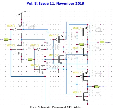
II. GDI ADDER
A new low power design technique that solves most of the problems is known as Gate-Diffusion-Input (GDI) method. This technique reduces power consumption, propagation delay, and area of digital circuits. GDI method is based on the use of a simple cell as shown in below figure. At the first look the design seems to be like an inverter, but the main differences are
1. GDI consist of three inputs- G (gate input to NMOS/PMOS), P (input to source of PMOS) and N (input to source of NMOS).
2. Bulks of both NMOS and PMOS are connected to N or P (respectively), so it can be arbitrarily biasedat contrast with CMOS inverter.
ISSN (Print) : 2320 – 3765 ISSN (Online): 2278 – 8875
I
nternational
J
ournal of
A
dvanced
R
esearch in
E
lectrical,
E
lectronics and
I
nstrumentation
E
ngineering
(A High Impact Factor, Monthly, Peer Reviewed Journal)
Website: www.ijareeie.com
Vol. 8, Issue 11, November 2019
Fig 2: Schematic Diagram of GDI Adder
This method is also suitable for designing fast, low-power circuits, using a less number of transistors, while improving logic level swing and static power characteristics and allowing simple top down design by using small cell library
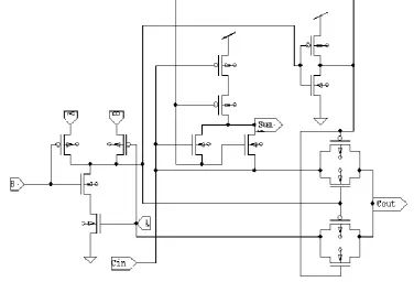
III. RBSD ADDER
RBSD numbers can be represented using the digit set (
1
,
0
,
1
) unlike binary number system, which is represented using binary digit set (0, 1). The decimal value of RBSD number can be calculated by following relation
10
2
n
i
i i
x
D
ISSN (Print) : 2320 – 3765 ISSN (Online): 2278 – 8875
I
nternational
J
ournal of
A
dvanced
R
esearch in
E
lectrical,
E
lectronics and
I
nstrumentation
E
ngineering
(A High Impact Factor, Monthly, Peer Reviewed Journal)
Website: www.ijareeie.com
Vol. 8, Issue 11, November 2019
Fig 3: Schematic Diagram of RBSD Adder
RBSD ADDER
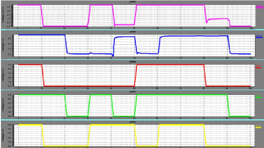
Simulated waveform of RBSD adder is shown below in fig 4.
ISSN (Print) : 2320 – 3765 ISSN (Online): 2278 – 8875
I
nternational
J
ournal of
A
dvanced
R
esearch in
E
lectrical,
E
lectronics and
I
nstrumentation
E
ngineering
(A High Impact Factor, Monthly, Peer Reviewed Journal)
Website: www.ijareeie.com
Vol. 8, Issue 11, November 2019
Parameters like delay and power dissipation is calculated at different VDD and at different VTH, which is shown in table 1 and table 2 respectively.
Table 1: Parameters of RBSD adder at different VDD
VDD(V)
Power Dissipation(mW)
Delay(nS)
Sum Cout
1.8 0.989 0.221 0.990 1.6 0.721 0.328 1.303 1.4 0.494 0.350 1.510 1.2 0.288 0.393 1.995 1.0 0.130 0.734 2.621
Table 2: Parameters of RBSD adder at different VTH
VTH(V) Power
Dissipation(mW)
Delay(nS)
Sum Cout
0.17 0.165 0.218 0.939 0.27 0.240 0.246 0.950 0.37 0.389 0.321 0.998 0.47 0.485 0.374 1.247 0.57 0.789 0.420 1.467
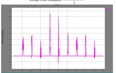
Simulated waveform of RBSD adder which is used for calculation of average power dissipation is shown in fig 5. Formula that is used for average power dissipation is given below
Average Power Dissipation =
2
min
max
P
P
ISSN (Print) : 2320 – 3765 ISSN (Online): 2278 – 8875
I
nternational
J
ournal of
A
dvanced
R
esearch in
E
lectrical,
E
lectronics and
I
nstrumentation
E
ngineering
(A High Impact Factor, Monthly, Peer Reviewed Journal)
Website: www.ijareeie.com
Vol. 8, Issue 11, November 2019
IV. CONCLUSION
In this paper adder has been designed and simulated using 180 nm CMOS technology of tanner tool at a various supply voltage from 1.0V to 1.8 V& compare their results with respect to various parameter. The comparison has been carried out both assuming circuits with minimum transistors size, to minimize the power consumption. Power consumption is a function of load capacitance, frequency of operation, and supply voltage. A reduction of any one of these is beneficial. A reduction in power consumption provides several benefits. Less heat is generated, which reduces problems associated with high temperature, such as the need for heat sinks. This provides the consumer with a product that costs less. In this paper we conclude that
The power consumption of GDI based adder is 50% less from RBSD adder but 26% less speed as compared to conventional RBSD adder.
Speed & power dissipation of CMOS adder is 10% & 39% less as compared to RBSD. Also CMOS adder has high noise margin as compared to other types of adders.
Layouts of these adders are also designed using Micro wind. From area comparison we see that area of GDI based adder is 11% less than RBSD adder.
REFERENCES
[1] N. Firake and S. Akashe, “Power-Delay Product Minimization of Mixed Full Adder Topologies for High-Performance”, African Journal of Computing & ICT, Vol 7. No. 2, pp: 93-98, ISSN 2006-1781, June, 2014.
[2] Ruchika Sharma and Rajesh Mehra, “Design of Error-Tolerant CMOS Adder Usingoptimized Transistor Count”, International Journal of Advanced Research in Computer and Communication Engineering, Vol. 3, Issue 7, ISSN (Print) : 2319-5940, July 2014.
[3] BaminGambo, Lod Tapin and Sarat Chandra Hanjabam, “ Low Power and High Performance Full Adder in Deep Submicron Technology”, Journal of Electronics and Communication Engineering Research Volume 2, Issue 3 pp: 07-16 ISSN : 2321-594, 2014 [4] Namarta and Mr. Sukhjit Singh, “ Comparative Analysis Different Adder Topologies using 180 nm Technology”, International Journal
for Science and Emerging Technologies with Latest Trends, Volume 14, Issue 1 pp: 07-11,ISSN No. : 2277-8136, 2014.
[5] S. Arif Basha & C. V. Subhaskara Reddy, “Low Power Highly Optimized Full Adder By Using Different Techniques With 10 Transistors”, International Journal of Engineering Research, Volume No. 3 Issue No: Special 2, pp: 95-96, ISSN:2319-6890, 22 March 2014.
[6] K Srinivas Raju and Dr. B. R. Vikram, “Competent Fetch Select Adder using 0.12 μm Expertise for Low Power Applications”, International Journal of Research in Modern Engineering and Emerging Technology, Vol. 2, Issue: 2, pp: 16-22,ISSN: 2320-6586, June-July 2014.
[7] Kandimalla Brahmani and Danda Aneesha, “Analysis of Full Adder Design using Various CMOS Design”, International Journal of Engineering & Science Research, Vol-4, Issue-7, pp:409-414, ISSN 2277-2685, July 2014.
[8] T. S. Ananth, A. Vijay and Dr. G.K.D. Prasanna Venkatesan, “Low-Power 1-Bit Full-Adder Cell using Enhanced Pass Transistor Logic and Power Gating”, International Journal of Advanced Technology in Engineering and Volume No. 02, Issue No. 06,pp:1-8 ISSN: 2348 – 7550 ,June 2014.
[9] V. Narayana Reddy and G. Sai Sindhu, “Design of Low Power 4 bit Ripple Carry Adder using DPTA synchronous Adiabatic Logic”, International Journal of Computational Science, Mathematics and Engineering, Volume 1, Issue 5, pp: 50-59, ISSN: 2349-8439, November 2014.
[10] Tran Bich Thuan Pham, Yi Wang and Renfa Li, “Designing one-bit Full-Adder/Subtractor based on Multiplexer and LUT’ sarchitecture on FPGA”, International Journal of Digital Content Technology and its Applications, Volume 7, Number 8, issue 8, pp: 454-464, April 2013.