Vol. 6, Issue 8, August 2017
A Soft Switching Converter with High Voltage
Gain and Amplified Efficiency for PV
Applications
Nadam Lavudya
Assistant Professor, Brilliant Group of Institutions, Ranga Reddy, Telangana India
ABSTRACT: This paper proposes a soft switching converter with high voltage gain for ac and dc photovoltaic applications. Day to day energy usage is snowballing significantly. Dc-Dc converters are the major consequence in renewable grid connected power applications because of the low voltage PV arrays. This shortcoming is overcome by using a novel soft switching dc-dc converter. This proposed concept is used to change the power efficiency by boosting voltage and also reduces the switching losses and efficiency. This problem is handled by using a high gain interleaved dc boost converter with capacitor and leakage inductor. A passive clamp network round the inductors affords the recapture of energy through leakage inductance leading to upgrading in the voltage gain and efficiency. The benefit of passive clamp network is that it condenses voltage stress on the switch. This proposed converter is designed and implemented by MATLAB/Simulation software and the results are results are validated.
KEYWORDS:voltage gain, bi directional DC-DC converter, Inverter,
I. INTRODUCTION
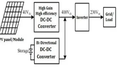
In the last few decades, there has been a drastic increase in the demand for electricity. This has led to rapid use and depletion of fossil fuels. These factors have led the researchers to renewable energy sources such as wind, solar PV and fuel cell stack. Solar Photovoltaic (PV) and fuel cell energy sources play a prominent role among the existing renewable sources poses major challenges such as optimal utilization of the source due to their non-linear characteristics (e.g. Maximum Power Point Tracking (MPPT) is required to track maximum available power from a PV source. They are usually operated at low output voltage levels (typ. 25-50V) because of safety issues. This makes their application to grid connected systems and even some stand-alone loads difficult because a large voltage boosting is required.A direct implication of points (a) and (b) is that the use of a dc-dc converter [1, 2] is essential at the front end, right across the source as shown in Fig. 1.
Fig. 1 Block diagram of a PV power conversion system
Vol. 6, Issue 8, August 2017
losses increase. Due to large duty cycle, the losses in parasitic resistances of inductance and capacitance also increase. Diode reverse recovery becomes a major concern. In view of the above, there is clearly a need to develop and use special high gain, high efficiency dc-dc converters to implement MPPT and to step up voltage level. Several circuit topologies have been proposed in the past [3-6] for this application. They follow one or more of the following philosophies to achieve high voltage at the converter output. (a)Direct voltage step-up using high frequency transformer. (b) Use of coupled inductor to utilize the energy storage capability of the magnetizing inductance of the core to increase the voltage level using turns ratio of the coupled inductor. (c) Use of interleaved coupled inductor that facilitates use of smaller inductors, division of current and higher effective inductance for higher power applications. (d) Active and passive clamp circuits to recover leakage energy in the coupled inductor based high gain converters to reduce losses in leakage inductance. (e) Use of intermediate energy storage capacitors as additional buffers to increase the voltage gain without increasing duty cycle to high value. A brief overview of the high voltage gain topologies reported in the literature is presented in the next section.
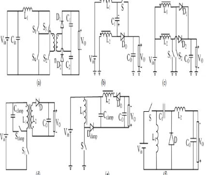
Fig. 2 Circuit diagrams of the high voltage gain dc-dc converters: (a) Isolated current-fed boost converter (b) Coupled inductor boost converter (c) Interleaved coupled inductor boost converter (d )Active clamp converter (e)Passive clamp converter (f) Intermediate Energy storage capacitor based
converter
II.OVERVIEW OF HIGH VOLTAGE GAIN DC-DCCONVERTER TOPOLOGIES
The converters shown in Fig. 2 depict some of the high voltage gain topologies that are representative of the existing configurations. Direct voltage step up using high frequency transformer renders a simple and easily controllable converter providing high gain. Isolated current-fed dc-dc converters [Fig. 2(a), [7-9] are example of this category. However these topologies result in high voltage spikes across the switch (due to leakage inductance) and large ripple in primary side transformer current as the turns ratio in the high frequency transformer increases. The isolated systems are relatively costly, bulky and generally less efficient [10] even though they offer more safety, eliminate issues such as ground leakage current and can provide multiple outputs among other advantages.
Vol. 6, Issue 8, August 2017
while passive clamp network [Fig. 2(e)] [4] consists of passive components such as diode, capacitor and resistor. The passive clamp circuit is more popular to reduce voltage stress across the converter switch by recycling leakage energy [17].
Voltage gain of the converter can be increased without increasing the duty cycle of the switch by connecting an intermediate capacitor in series with the inductor [Fig. 2(f)]. The intermediate energy storage capacitor with coupled inductor charges in parallel and discharges in series with the coupled inductor secondary. Various principles discussed in preceding paragraphs have also been used in combinations to achieve high voltage gain and enhanced features. A coupled inductor type boost converter has been used in association with a passive clamp circuit to achieve high gain and increased efficiency. Converter configurations with coupled inductor in association with a voltage multiplier circuit and/or intermediate capacitor have also been reported to achieve high voltage gain. In recent times, use of coupled inductors along with intermediate capacitors has also become popular. Keeping in mind the merits and demerits of the various schemes described in preceding paragraphs, a novel topology has been proposed in this paper that achieves high voltage through a coupled inductor connected in interleaved manner that charges an intermediate buffer capacitor and a passive clamp network to recover the leakage energy. Coupled inductor leads to the incorporation of 'turn‟s ratio' into the gain expression that leads to high efficiency without increasing the duty ratio. As compared to existing high gain dc-dc converters, the number of passive components used in the proposed converter is less, which reduces the cost and improves the efficiency. Though the proposed converter is applicable to any low voltage source application (e.g. solar PV, Fuel cell stack, battery etc.), this paper focuses only on the solar PV source. All the details of this work are presented in the subsequent sections of the paper.
III. DESCRIPTION OF THE PROPOSED CONVERTER
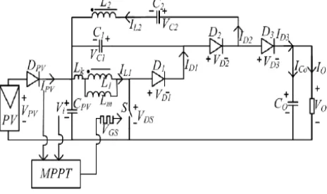
Energy conversion efficiency of solar PV is quite low (about 12–25%) [24]. Therefore, it is essential to use a highly efficient power conversion system to utilize the PV generated power to the maximum. The proposed high gain dc-dc converter configuration is shown in Fig. 3.
Fig. 3 Circuit diagram of proposed dc-dc converter
Vol. 6, Issue 8, August 2017
The gain ratio, n is given by:
𝑛 =𝑉𝐿2 𝑉𝐿1
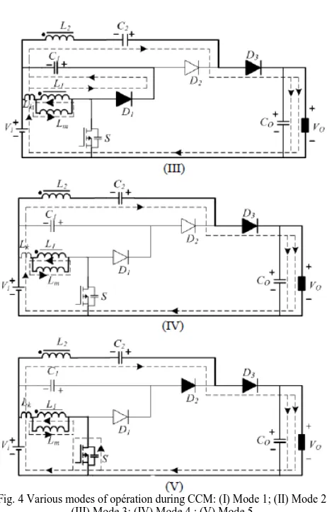
Where, VL1 and VL2 represent the voltages across inductors L1 and L2. The operating modes for continuous conduction mode (CCM) are shown in Fig. 4. Various operating modes are described below:
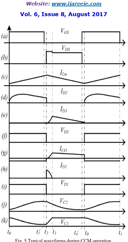
Mode 1[t0-t1]: The switch (S) is turned on at the start of the converter operation. The current flows through the switch and the primary side of the coupled inductor (L1), energizing the magnetizing inductance (Lm) of the coupled inductor. The current path is as shown in Fig. 4(I).
Vol. 6, Issue 8, August 2017
Fig. 4 Various modes of opération during CCM: (I) Mode 1; (II) Mode 2; (III) Mode 3; (IV) Mode 4 ; (V) Mode 5.
Mode 3[t2-t3]: In this mode, diodes D1 and D3 become forward biased. D2 is reverse biased and its current becomes zero in this mode. The leakage energy stored in the primary side of the coupled inductor (L1) is recovered and stored in the clamp capacitor (C1) through D1. Also, the energy is transferred from the input side to the output side through diode D3 as shown in Fig. 4(III).
Mode 4[t3-t4]: This mode begins after the completion of recovery of the leakage energy from inductor L1. The diode D1 now becomes reverse biased while diode D3 remains forward biased in this mode. The current flows from the input side to the output side to supply the load as shown in Fig. 4(IV).
Vol. 6, Issue 8, August 2017
Fig. 5 Typical waveforms during CCM operation.
Vol. 6, Issue 8, August 2017
Fig.7. Voltage across diode d1, d2, d3.
Fig.8. Output voltage of the solar PV system
Fig.9. AC Output Current.
Vol. 6, Issue 8, August 2017
Fig.11. Efficiency versus load curve for the proposed dc-dc converter and comparison with existing versions;
Efficiency plot with respect to load variation of the proposed converter is shown in Fig. 8(i). The efficiency plot of the proposed converter is compared with conventional push-pull converter having identical input output voltage ratings (Vi=40V; Vo=400V) and operating frequency (50kHz). Full load (400W) efficiency of the converter, obtained from experimentation, is 96% (maximum ≈ 97% at lighter load). A comparison is also shown with conventional, hard switched push pull converter (of identical rating, operating frequency and input/output voltage specifications) with and without active clamp across the main switch. The proposed system shows a higher efficiency under all load conditions.
V.CONCLUSION
The high gain, high frequency converter proposed in this paper is suitable for low output voltage sources such as solar PV, fuel cell stack and battery. The circuit efficiency can be achieved nearly 96%. The proposed converter has turns ratio of inductor around 4 or 5 and duty cycle may be 0 to 0.7. High voltage gain is achieved without extreme duty cycle. The reason for high efficiency is reduction in switching losses. Moreover high gain design is implemented to achieve higher value of output voltage. The major advantage of proposed converter is that it is applicable for both AC and DC loads.
REFERENCES
[1] W. Li, and X. He, “Review of Non-isolated High-Step-Up DC/DC Converters in Photovoltaic Grid-Connected Applications,” IEEE Trans. Ind. Electron., vol. 58, no. 4, pp. 1239-1250, April 2011.
[2] E. Mamarelis, G. Petrone, G. Spagnuolo, "Design of a Sliding-Mode- Controlled SEPIC for PV MPPT Applications," IEEE Trans. Ind. Electron., vol. 61, no. 7, pp. 3387-3398, July 2014.
[3] K. W. Ma and Y. S. Lee, “An integrated fly-back converter for dc uninterruptible power supply,” IEEE Trans. Power Electron., vol. 11, pp. 318– 327, March 1996
[4] Q. Zhao and F. C. Lee, “High-efficiency, high step-up dc-dc converters,” IEEE Trans. Power Electron., vol. 18, no. 1, pp. 65–73, Jan. 2003. [5] G. C. Silveira, F. L. Tofoli, L. D. S. Bezerra and R. P. Torrico- Bascope, "A Nonisolated DC–DC Boost Converter With High Voltage Gain and Balanced Output Voltage," IEEE Trans. Ind. Electron., vol. 61, no. 12, pp. 6739-6746, Dec. 2014
[6] C. T. Pan, C. F. Chuang and C. C. Chu "A Novel Transformer-less Adaptable Voltage Quadrupler DC Converter with Low Switch Voltage Stress", IEEE Trans. Power Electron., vol. 29, no. 9, pp. 4787-4796, Sept. 2014.
[7] J. H. Lee, T. J. Liang and J. F. Chen, "Isolated Coupled-Inductor- Integrated DC–DC Converter With Nondissipative Snubber for Solar Energy Applications," IEEE Trans. Ind. Electron., vol. 61, no. 7, pp.
3337-3348, July 2014.
[8] P. Xuewei and A. K. Rathore, "Novel Bidirectional Snubberless Naturally Commutated Soft-Switching Current-Fed Full-Bridge Isolated DC/DC Converter for Fuel Cell Vehicles," IEEE Trans Ind. Electron., vol. 61, no. 5, pp. 2307-2315, May 2014.
[9] C. T. Choi, C. K. Li, and S. K. Kok, "Modeling of an active clamp discontinuous conduction mode flyback converter under variation of operating conditions," in Proc. IEEE PEDS, vol. 2, pp.730-733, 1999.
[10]M. Prudente, L. L. Pfitscher, G. Emmendoerfer, E. F. Romaneli and R. Gules, "Voltage Multiplier Cells Applied to Non-Isolated DC–DC Converters," IEEE Trans. Power Electron., vol. 23, no. 2, pp. 871-887, Mar. 2008.
Vol. 6, Issue 8, August 2017
[15]M. Kwon and B. H. Kwon, "High Step-Up Active-Clamp Converter with Input-Current Doubler and Output-Voltage Doubler for Fuel Cell Power Systems," IEEE Trans. Power Electron., vol. 24, no. 1, pp. 108- 115, Jan. 2009.
[16]K. C. Tseng and C. C. Huang, "High Step-Up High-Efficiency Interleaved Converter With Voltage Multiplier Module for Renewable Energy System," IEEE Trans. Ind. Electron., vol. 61, no. 3, pp. 1311- 1319, Mar. 2014.