A Model of DC-AC 1-Ø Resonant Inverter Using Soft
Switching Boost Converter and with a Prototype
Mr.A.Sreenivasulu1,Mr. D VenkataBramhanaidu2 1, 2
Department of Electrical and Electronics Engineering, SVU College of Engineering, Tirupati, AP, India.
Abstract: In this paper, a novel DC-AC single phase inverter is proposed. When the switches are turned on and off, a conventional inverter generates switching loss because of the hard switching. Thus, the inverter loss is increased. Proposed system contains auxiliary circuit. The converter stage switches perform soft-switching because of the auxiliary circuit. Also inverter stage switches perform ZVS when the dc-link voltage is zero. Therefore all switches perform soft-switching when the switches are turned on and off. Thus the proposed system reduces switching loss and voltage stress. A modifying Prototype DC- AC single phase resonant inverter consists of soft switching boost converter and H-Bridge inverter is presenting.
I. INTRODUCTION
Nowadays, the power electronics are required to develop smaller, lighter, less expensive and reliable system. In order to operate these systems, a switching frequency has to be increased. But, increasing the inverter switching frequencies is dependent on the advances in device technology and makes higher switching losses. [1], [2].
To solve this problem, the soft switching techniques have been adopted in the inverter circuit. By the soft-switching techniques, the switching losses are ideally zero and the switching frequencies can be increased to above the audible range. In this paper, a novel DC-AC single phase resonant inverter using soft switching boost converter is proposed. This proposed inverter consists of soft-switching boost converter and H-bridge inverter. The soft-soft-switching boost converter in proposed inverter additionally has resonant inductor Lr, resonant capacitor Cr, bridge diode and auxiliary switch Q2. When the resonance between resonant inductor and capacitor is generated, the converter switches are turned on and off with soft-switching. Also H-bridge inverter switches are turned on and Off with ZVS when the auxiliary switch is turned off. So all of the switches are turned on and off with soft-switching. [3], [4], [5], [6] Therefore the novel DC-AC single phase resonant inverter using soft-switching boost converter can reduce the switching loss and voltage stress. In this paper, we have analysed the operational principle of the proposed resonant inverter. Simulation results presented to confirm the theoretical analysis.
II. PROPOSED INVERTER
Fig. 1 Proposed novel DC-AC single phase resonant inverter using soft switching boost converter
( ~ )( ~ )( ~ )
[image:3.612.57.533.70.371.2]( ~ )( ~ )( ~ )
Fig. 2 Operation mode diagrams for the novel DC-AC single phase resonant inverter using soft-switching boost converter
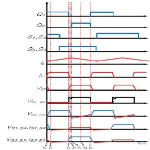
Fig.3 Operation waveforms for the novel DC-AC single phase resonant inverter using soft-switching boost converte
[image:3.612.150.444.406.701.2]Mode 1 (t0 t<t1): The resonant capacitor is discharged through resonant path Cr and Lr. The resonant inductor current begins to
increase linearly from zero. Therefore, the main switch is turned on with ZCS influenced by resonant inductor. The energy of the main inductor is delivered to the load through the switches (S1, S4).
The next mode is started as soon as the resonant capacitor has fully discharged. In this mode, the main inductor current is given by
( ) = ( ) + ( − ) ………. (1)
( )≅ ≅ ( ) ………. (2)
Initial resonant inductor current and capacitor voltage given by
( )≌0 ………... (3)
( )≌ ………... (4)
The resonant period is
= ………... (5)
The resonant impedance is
= ………... (6)
The inductor current and resonant capacitor voltage in resonant period are given by,
( ) = ( − ) + cos ( − ) + sin ( − ) …..(7)
( ) = cos ( − )− sin ( − ) ...……..(8)
Mode 2 (t1 t<t2): When the resonant capacitor is fully discharged to Mode1, the anti-parallel diodes in inverter switches constitute
current path. At this time, the inverter stage is zero. When the inverter stage is in the zero voltage condition, the inverter switches are given to PWM signal (S1, S4). So, inverter switches are turned on and off with ZVS. This mode isG maintained when the main
switch is turned-off. The main inductor current is given by
( ) = ( ) + ( − )………...(9)
The resonant inductor current and resonant capacitor voltage are given by
( )≌ ( )≌ ( ) ……….…. (10)
( )≌ ( )≌0V………... (11)
Mode 3 (t2˺ t<t3): When the switch is turned off with ZVS, the resonant inductor releases energy. Thus, the bridge diode is turned on. The dc-link capacitor is transferred to main inductor and resonant inductor energy through the bridge diode. The resonant capacitor starts to charge main inductor energy. At that time, the resonant inductor current and resonant capacitor voltage are given by
( ) = + − cos ( − )− ( )sin ( − )…….(12)
( ) = − cos ( − ) + − − ( ) sin ( − )………..….(13)
( )≌0 ………... (14)
In this mode, the main inductor current is given by
( ) = ( )− ( − ) ……….………. (15)
( )≌ ……….………. (16)
Mode 4 (t3˺ t<t4): When the resonant inductor energy is fully released, the bridge diode is turned-off. This mode is maintained until the resonant capacitor voltage becomes 400[V]. The main inductor current flows continuously through the inverter switches (S1, S4). In this mode, resonant capacitor voltage is given by
( ) = ( − ) + ( )……… (17)
( )≌ ………...……. (18)
Resonant inductor current is given by
( )≌ ( )≌0 ………...………. (19)
Mode 5 (t4 ื t<t5): This mode is started when the resonant capacitor is fully charged. After that, the auxiliary switch is turned on
charged from the main inductor energy. Because the main inductor current flows through the anti-parallel diode, the auxiliary switch voltage is zero voltage. When the auxiliary switch current path is changed, the next mode starts. In this mode, the main inductor current can be expressed as
( ) = ( )− ( − )……… (20)
Mode 6 (t5 ื t<t6): In this mode, the auxiliary switch current path is changed because the dc-link capacitor starts to discharge. Therefore, the load is supplied the energy by the dc-link capacitor and main inductor. This mode maintains that the main inductor current equal to the resonant current. The main inductor current in this mode is expressed as ( ) = ( )− ( − )……….... (21)
( )≌ ……… (22)
( )≌ ( )≌0 ………….………... (23)
( )≌ ………….………... (24) After this mode ends, returning the mode 1
IV. SIMULATION RESULT
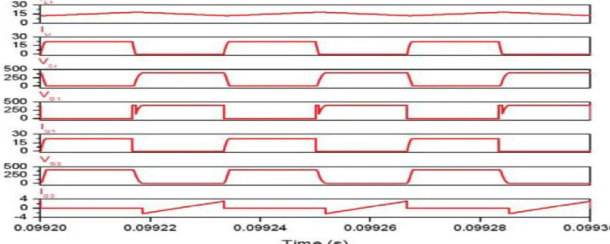
This proposed resonant inverter is simulated to demonstrate the features and theoretical analysis. A 3kW prototype resonant inverter is built and simulated using the PSIM tool. The parameters used for simulations are as follow TABLE1
TABLE1. Simulation parameters
V
dc 200[V]
V
dc-link 400[V]
Main inductor 1000[ μ H]
Resonant inductor 10[ μ H]
Resonant capacitor 10[nF]
DC-Link-Cap 1000[ μ F]
Con. Switching Freq. 30[kHz]
Inv. Switching Freq. 15[kHz]
[image:5.612.93.520.511.682.2]Fig. 4 shows simulation waveforms of converter stage in resonant DC-AC single phase inverter. During the resonance period between the resonant inductor and the resonant capacitor, the main switch and auxiliary switch are turned on and off with ZVS and ZCS.
Fig.5 Principle operation waveforms of the proposed resonant inverter
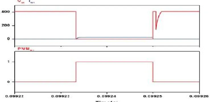
Fig. 6 The waveforms of the voltage and the current of the main switch at turned-on and off with ZVS
Fig. 8The waveforms of the voltage and the current of the inverter switch at turned-on and off with ZVS
Fig. 5 presents principle operation waveforms of the proposed resonant inverter. When the switch current in inverter stage flows through the anti-parallel diode of inverter switch, the inverter switches maintain the freewheeling mode. Therefore, all inverter switches perform the soft-switching under the zero voltage condition.
Fig.6 shows the main switch waveforms of the voltage and the current when the switch is turned and off with ZVS. Fig.7 shows the waveforms of the voltage and the current of the auxiliary switch at turned-on and off with ZVS.
During the resonant period, the bridge diode is turned on. At this time, dc-link capacitor is charged from resonant inductor energy when the current flows through the anti-parallel diode of auxiliary switch. Therefore, the auxiliary switch has zero-voltage condition. At this time, the switch is turned on with ZVS.
Fig. 8 presents the waveforms of the voltage and the current of the inverter switch at turned-on and off with ZVS. All inverter switches have freewheeling mode, under the zero voltage condition. After this mode ends, returning the mode 1.
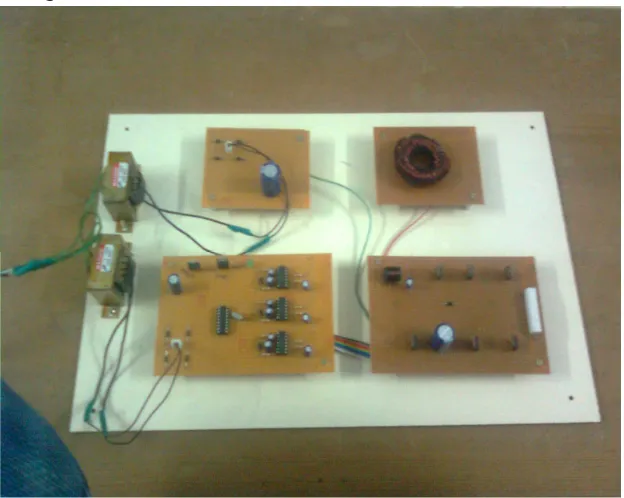
V. PROTOTYPE CIRCUIT AND RESULTS
[image:7.612.97.533.80.256.2]A prototype is designed by using the control circuit as shown in the Fig.5.4 with a specified load values at input 15V and switching frequency 10 kHz, as shown in Fig.5.5
[image:7.612.153.465.453.702.2]DC input voltage from the prototype circuit is 15v
Fig.5.6 DC input voltage
[image:8.612.171.447.335.513.2]The triggering pulse for the switch S1 is shown in Fig. 5.7
Fig 5.7 Switching pulse S1
[image:8.612.165.449.536.719.2]A 30V rms ac voltage is obtained across the resistance RL its frequency 20 kHz as shown in Fig. 5.7
VI. CONCLUSION
In this paper, we proposed a novel DC-AC single phase resonant inverter using soft-switching boost converter. In this topology, all switches perform a soft switching by resonance between the resonant inductor and capacitor. So, the proposed topology can reduce the switching loss and voltage stress. The proposed inverter is analysed through the operation mode, and its validity is proven through simulation.
The 15V DC is step up to 30V. The DC is converted into AC using single phase inverter. The pluses required by the MOSFETS, are generated using PIC micro controller. These pulses are amplified by using driver circuit. This circuit has advantages like reduced hardware and improves response. The experimental results are compared with simulation results.
REFERENCES
[1] D. M. Divan, G. Skibinski, ˈ Zero switching loss inverters for high power applications,ˉ IEEE IAS Rec., pp. 627-634, 1987.
[2] S.R. Park, S.H. Park, C.Y. Won, Y.C. Jung, "Low loss soft switching boost converter", 2008 13th International Power Electronics and Motion Control Conference (EPE-PEMC 2008) pp. 181 - 186. 2008
[3] K. Wang, G. Hua, and F. C. Lee, ˈ "Analysis, design and ZCS-PWM boost converters” in Proc. IEEJ Int. Power Electronics Conf., pp.1202-1207, 1995 [4] G. Hua, X. Yang, Y. Jiang, and F.C. Lee, “Novel zero-current-transition PWM converter”, IEEE Power Electronics Specialist Conf. Rec., pp. 538~544, 1993. [5] H. Ohashi, ‘‘Power Electronics Inovation with Next Generation Advanced Power Devices’’, Proceeding of INTELEC'03, Oct.2003, Yokohama (Japan), pp.9-13 [6] D. M. Divan and G. Skibinski, “Zero switching loss inverters for high power applications,” IEEE IAS Rec., pp. 627-634, 1987
Author Profile
Mr. A.Sreenivasulu was born in Andhrapradesh, India, He received his B.Tech degree in Electrical and Electronics
Engineering from JNTU in 2008. He received his M.Tech in Power Electronics from JNTU Anatapuram in 2011. Pursuing Ph.D. in Annamalai University. His areas of interests are Power Electronics and Electrical Drives.