Radial pn Junction, Wire Array Solar Cells
Thesis by
Brendan Melville Kayes
In Partial Fulfillment of the Requirements for the Degree of
Doctor of Philosophy
California Institute of Technology Pasadena, California
2009
ii
c 2009
iv
Acknowledgements
I was recently reminded of an email I sent to my parents way back in January 2003, in the core of which I wrote “I just spoke to Harry Atwater on the phone while he was driving to Boston from NYC, and him [sic] and Nate have put their heads together and cooked me up what looks like a beauty of a research project. Basically, Harry wants me to design and work out how to build and I guess hopefully build a third generation silicon cell which will take the manufacturing experience of his silicon lab and marry it with the exciting new possibilities afforded by recent work in chemical solar cells. So, apparently, truly somewhere in between Nate’s and Harry’s work, while still allowing me to keep my feet firmly planted in “Applied Physics” (and thus avoid that dirty world of Chemistry). He was talking [about] getting me an office, starting to review papers with me, learning semiconductor device physics over the summer, . . .I’m super excited”. I make no claim to have worked on a “third generation” [1] device in this thesis, but other than that I’m struck by how little has changed since then (particularly with regards to Harry’s ever-busy travel schedule).
First and foremost I would like to acknowledge the guidance and support of my two advisors, Harry Atwater and Nate Lewis. I don’t even know where to begin, except to say that virtually everything I know about that which I’m now trying to make a career out of, namely semiconductors, solar energy conversion, etc. etc. etc., I owe it to these two men. Their encouragement, the challenges they have set for me, the insights, the opportunities -all have contributed to making me feel truly like a different person from who I was when I arrived at Caltech.
I would like to thank my candidacy and thesis committees, which, in addition to my advisors, have been composed of Marc Bockrath, Oskar Painter, Ken Pickar, and Rachid Yazami in various combinations. I would also like to thank all of the other Caltech faculty from whom I took classes while here. Particularly I would like to acknowledge the great teaching skills of Alan Weinstein, Oskar Painter, and Rob Phillips.
I would like to give a big “gracias” to the people at BP Solar, particularly Dave Carlson, Nigel Mason, Juan Manuel Fernandez, In´es Vincueria, and all the people in the Technology group at BP Solar Tres Cantos, both for encouragement and advice along the way, and also for the opportunity to intern at BP Solar.
I am indebted to all of “team nanowire”, namely Mike Filler, Mike Kelzenberg, Jim Maiolo, Stephen Maldonado, Kate Plass, Morgan Putnam, Josh Spurgeon, and the “new-comers” Leslie O’Leary, Dan Turner-Evans, and Emily Warren. I feel the need to single out Prof. Dr. Mike Filler for particular thanks. This thesis would be a very different thing had he not joined the Atwater group as a postdoc two years ago, and his tenacity, discipline, knowledge and intuition have been an inspiration for me. Thanks also to my SURF stu-dent Tom Sadler. Also I would like to thank Melissa Archer, Krista Langeland, Christine Richardson, Katsu Tanabe, and Jimmy Zahler for their help and insight into other aspects of PV.
There are many other people who have helped me in large and small ways in lab through-out my time here (apologies if I forget anyone) - Andrea Armani, Deniz Armani, Julie Biteen, Ryan Briggs, Stanley Burgos, Hsin-Ying Chiu, Jinsub Choi, Vikram Deshpande, Matt Dicken, Ken Diest, Jen Dionne, Edgardo Garc´ıa-Berr´ıos, Florian Gstrein, Hossam Haick, Dave Henry, Pieter Kik, Sungjee Kim, Greg Kimball, Dave Knapp, Andrew Leen-heer, Henri Lezec, Dave Michalak, Gerald Miller, Keisuke Nakayama, Joe Nemanick, Deirdre O’Carroll, Domenico Pacifici, Young-Bae Park, Jen Ruglovsky, Luke Sweatlock, Chee-Seng Toh, Matt Traub, Robb Walters, Lauren Webb, and Marc Woodka.
I would like to thank the entirety of the Atwater and Lewis groups (too many to list here?). Particularly, and on a more personal note, thanks to Mike Filler, Krista Langeland, Christine Richardson, Jen Ruglovsky, and Robb Walters, for making the lab a more enjoy-able place to be. Thanks also to my office-mates, Jimmy Zahler, Jen Dionne, Gerald Miller, Krista Langeland, and Darci Taylor.
vi
Warehouse, and all of the folks at Shipping & Receiving; the folks at the Chemistry machine shop, and Rick Gerhart in the glass shop; all of the staff in all of the different shops and trades; all the staff of the various stockrooms; the janitorial staff for keeping Watson from getting too chaotic; and all of the staff in Caltech Dining Services, and Ernie, for feeding me.
Personally, I would like to thank Dan Braun and Jeff Price for being my best friends in the past few years, and for many more into the future I am sure. Thanks to my non-Atwater/Lewis Caltech friends, particularly Eugene Mahmoud and James Maloney, both of whose careers I will watch with keen interest. Much respect to all of the people who worked, and continue to work, in ways large and small with Engineers for a Sustainable World @ Caltech while I was involved with it, as well as after I left. In particular, in addition to Eugene, I would like to thank Nathan Chan, Janet Hering, Sera Linardi, Ken Pickar, Tim Prestero, Derek Rinderknecht, and John Van Deusen. Thanks to my L.A./N.Z. hybrid friends, namely John Marshall and John Phillips. Thanks to Christina Bianchi for trying to keep me sane recently, with arguable success. Thanks to all of my other L.A. friends, for making it fun. Thanks to my other New Zealand friends, near and (mostly) far, particularly Niki Bogle, Duncan Greive, Brody Nelson, and Mike “Zeke” Simperingham. And my t’ai chi teachers and friends, particularly Rob Lindsay, Bob Goodwin, Yan Yuanhua, Craig Cottrell and Walter Rodriguez, unspeakable gratitude to you all.
Last but certainly not least, to my family, particularly my parents - I truly could not have done this without your love and support. Thank you.
Brendan Kayes
August 2008
Abstract
Radial pn junctions are potentially of interest in photovoltaics as a way to decouple light absorption from minority carrier collection. In a traditional planar design these occur in the same dimension, and this sets a lower limit on absorber material quality, as cells must both be thick enough to effectively absorb the solar spectrum while also having minority-carrier diffusion lengths long enough to allow for efficient collection of the photo-generated carriers. Therefore, highly efficient photovoltaic devices currently require highly pure materials and expensive processing techniques, while low cost devices generally operate at relatively low efficiency.
The radial pn junction design sets the direction of light absorption perpendicular to the direction of minority-carrier transport, allowing the cell to be thick enough for effective light absorption, while also providing a short pathway for carrier collection. This is achieved by increasing the junction area, in order to decrease the path length any photogenerated minority carrier must travel, to be less than its minority carrier diffusion length. Realizing this geometry in an array of semiconducting wires, by for example depositing a single-crystalline inorganic semiconducting absorber layer at high deposition rates from the gas phase by the vapor-liquid-solid (VLS) mechanism, allows for a “bottom up” approach to device fabrication, which can in principle dramatically reduce the materials costs associated with a cell.
viii
Contents
List of Figures xii
List of Tables xv
List of Publications xvi
1 Introduction 1
1.1 Energy, Climate Change, and Photovoltaics . . . 1
1.2 Production of Si for Photovoltaics . . . 3
1.3 Orthogonalizing Light Absorption and Carrier Transport . . . 5
1.4 Nanowires and Vapor-Liquid-Solid Growth . . . 10
1.5 The Radial pn Junction, Wire Array Solar Cell . . . 11
2 Solar Cell Device Physics and the Radial Geometry 13 2.1 Introduction . . . 13
2.2 “To First Order”: Salient Features . . . 13
2.3 Transport Equations in the Radial Geometry . . . 20
2.3.1 Quasineutral Regions . . . 24
2.3.2 Depletion Region . . . 26
2.3.3 Solution . . . 26
2.4 Numerical Assessment of Device Behavior in Si . . . 28
2.4.1 Preliminary Observations . . . 30
2.4.2 Simulation Parameters . . . 35
2.4.3 Quasineutral Region Recombination Dominated Analysis . . . 36
2.5 Application to Direct Band Gap Semiconductors . . . 43
2.6 Axial pn Junction Wire Solar Cells . . . 47
2.7 Conclusion . . . 49
3 Vapor Liquid Solid Growth of Si Wires from SiH4 53 3.1 Introduction . . . 53
3.2 The Vapor-Liquid-Solid (VLS) Process . . . 53
3.3 Catalyst Selection . . . 54
3.3.1 VLS Thermodynamics . . . 55
3.3.2 Temperature Requirements . . . 56
3.3.3 Effect of Catalyst on Optoelectronic Properties of Si . . . 56
3.3.4 Additional Effects of Catalysts Highly Soluble in Solid Si . . . 59
3.3.5 Cost and Availability of Catalyst . . . 60
3.3.6 Oxidation . . . 61
3.4 Results from VLS Growth with SiH4 . . . 61
3.4.1 TEM of SiH4-grown Wires . . . 65
3.5 Single Wire Electrical Measurements . . . 66
3.6 Patterned Growth . . . 68
3.7 Axial Heterostructures . . . 72
3.8 Conclusion . . . 74
4 Growth of Si Wire Arrays from SiCl4 76 4.1 Introduction . . . 76
4.2 SiCl4 and Catalyst Choice . . . 77
4.3 Unpatterned VLS Growth . . . 77
4.3.1 Catalyst Selection . . . 77
4.3.2 Growth from Nanoparticles . . . 81
4.3.3 TEM of SiCl4-grown Wires . . . 82
4.4 Patterned VLS Growth . . . 82
4.5 Effects of Temperature . . . 86
4.6 Changing VLS Growth Catalyst . . . 86
4.7 Changing Wire Diameter and Pitch . . . 89
x
4.7.2 10 μm Pattern . . . 93
4.8 Conclusion . . . 96
5 Device Fabrication and Photovoltaic Measurements of Wire Arrays 98 5.1 Introduction . . . 98
5.2 Fabrication of a Device Using Grown Wires . . . 98
5.2.1 Catalyst Removal . . . 98
5.2.2 Doping: Radial pn Junction Formation . . . 99
5.2.3 Metallization . . . 101
5.3 Characterization of VLS-grown Samples . . . 101
5.4 Previous Fabrication Attempts . . . 107
5.4.1 Previous Fabrication Attempts - I . . . 107
5.4.2 Previous Fabrication Attempts - II . . . 109
5.5 Fabrication of a Device Using Reactive Ion Etching . . . 111
5.6 Characterization of Devices from Reactive Ion Etched Samples . . . 113
5.7 Conclusion . . . 116
6 Outlook 117 6.1 Towards a Solid-State, Flexible, Single-Crystalline Si PV Device . . . 117
6.2 Other Applications of Si Wire Arrays . . . 118
6.3 Conclusion . . . 119
A MatLab Simulation Code 122 A.1 Radial pn Junction Simulation . . . 122
A.1.1 depletionregion.m . . . 133
A.1.2 depletion.m . . . 135
A.2 Planar pn Junction Simulation . . . 136
A.3 Axial pn Junction Wire Simulation . . . 147
A.3.1 axialdifferencebottom.m . . . 149
A.3.2 axialdifferencetop.m . . . 153
B Radial pn Junction, Wire Array Solar Cell Fabrication 157 B.1 Radial pn Junction, Wire Array Solar Cell Fabrication . . . 157
B.1.2 Wire Growth . . . 158
B.1.3 Catalyst Removal . . . 159
B.1.4 Doping: Radial pn Junction Formation . . . 159
B.1.5 Metallization . . . 160
xii
List of Figures
1.1 Planar solar cell schematic . . . 6
1.2 VMJ solar cell schematic . . . 7
1.3 PMJ solar cell schematic . . . 9
1.4 Radial pn junction, wire array solar cell schematic . . . 11
2.1 The AM 1.5 global spectrum . . . 15
2.2 Relative absorption of sunlight Si and GaAs . . . 17
2.3 Absorption of sunlight by Si and GaAs . . . 18
2.4 Generalized band structure . . . 21
2.5 Schematic of a single wire from the radial pn junction cell . . . 23
2.6 Schematic of a conventional planar pn junction cell . . . 24
2.7 Efficiencyη,Jsc, and Voc, versus Land R for a radial pn junction cell . . . 32
2.8 Efficiencyη,Jsc, and Voc, versus Land R for a radial pn junction cell . . . 33
2.9 Efficiencyη,Jsc, and Voc, versus Land R for a radial pn junction cell . . . 34
2.10 Comparison of Jsc in planar and radial geometries, in quasineutral region recombination dominated regime . . . 36
2.11 Comparison of Voc in planar and radial geometries, in quasineutral region recombination dominated regime . . . 37
2.12 Comparison of F F in planar and radial geometries, in quasineutral region recombination dominated regime . . . 38
2.13 Comparison of efficiency in planar and radial geometries, in quasineutral region recombination dominated regime . . . 39
2.15 Comparison of F F in planar and radial geometries, in depletion region
re-combination dominated regime . . . 41
2.16 Comparison of efficiency in planar and radial geometries, in depletion region recombination dominated regime . . . 41
2.17 Comparison of Jsc in planar and radial geometries . . . 44
2.18 Comparison of Voc in planar and radial geometries . . . 45
2.19 Comparison of efficiency in planar and radial geometries . . . 45
2.20 Effect of surface recombination velocity on axial junction carrier concentration 50 3.1 Trap levels in Si . . . 57
3.2 Earth abundance of the chemical elements . . . 60
3.3 Au catalyzed Si wires, grown from SiH4 . . . 62
3.4 Al catalyzed Si wires, grown from SiH4 . . . 63
3.5 Ga catalyzed Si wires . . . 63
3.6 In catalyzed Si wires . . . 64
3.7 Partial phase diagram of growth of Si nanowires from In catalyst . . . 65
3.8 Composite TEM image of SiH4 grown . . . 67
3.9 TEM image showing presence of Au on SiH4-grown Si wire surface . . . 68
3.10 High resolution TEM image of Au-catalyzed, SiH4-grown Si wire . . . 69
3.11 Electrical contacts to single Si wires . . . 70
3.12 Four-point probe measurement of a single Si wire . . . 70
3.13 Au-catalyzed, SiH4-grown Si wires, patterned by electron beam lithography 72 3.14 In-catalyzed, SiH4-grown Si wires, patterned by electron beam lithography . 73 3.15 Ge on Si heterostructures . . . 74
4.1 SEM image of Au-catalyzed Si wire growth . . . 78
4.2 Representative SEM images of wire growth from evaporated Au, Cu and Ni films . . . 79
4.3 SEM images of Al-catalyzed Si wire growth . . . 80
4.4 SiCl4 growth from Au nanoparticles . . . 81
4.5 TEM image of a Au-catalyzed Si nanowire . . . 83
4.6 TEM images of the tips of Au-catalyzed Si nanowire . . . 84
xiv
4.8 Au-catalyzed Si wire array . . . 87
4.9 Degradation of oxide pattern at high growth temperatures . . . 88
4.10 Cu-catalyzed Si wire array . . . 90
4.11 Ni-catalyzed Si wire array . . . 91
4.12 Representative SEM images of 2 and 5 μm patterns . . . 94
4.13 Representative SEM images of 10 μm patterns . . . 96
4.14 Representative SEM images of 10 μm patterns patterned by RIE . . . 97
5.1 Doping profile of SOI planar control . . . 102
5.2 Schematic of VLS-grown wire cell . . . 103
5.3 Light and darkJ-V of VLS-grown wire cell . . . 103
5.4 Schematic of first attempt at VLS-grown wire cell . . . 108
5.5 Light and darkJ-V of first attempt at VLS-grown wire cell . . . 109
5.6 Schematic of second attempt at VLS-grown wire cell . . . 110
5.7 RIE-fabricated Si wire array PV cell . . . 113
5.8 Voc vs. junction area . . . 114
List of Tables
2.1 Comparison of the basic features of the planar and radial geometries . . . . 19
xvi
List of Publications
Portions of this thesis have been drawn from the following publications:
Radial pn junction, wire array solar cells. B. M. Kayes, M. A. Filler, M. D. Henry, J. R. Maiolo, M. D. Kelzenberg, M. C. Putnam, J. M. Spurgeon, K. E. Plass, A. Scherer, N. S. Lewis, and H. A. Atwater, Conference Record of the Thirty-third IEEE Photovoltaic Specialists Conference (2008)
Growth of vertically aligned Si wire arrays over large areas (>1 cm2) with Au and Cu cata-lysts. B. M. Kayes, M. A. Filler, M. C. Putnam, M. D. Kelzenberg, N. S. Lewis, and H. A. Atwater, Applied Physics Letters 91, 103110 (2007)
Synthesis and characterization of silicon nanorod arrays for solar cell applications. B. M. Kayes, J. M. Spurgeon, T. C. Sadler, N. S. Lewis, and H. A. Atwater, Conference Record of the IEEE 4th World Conference on Photovoltaic Energy Conversion1, 221 (2006)
Comparison of the device physics properties of planar and radial p-n junction nanorod solar
cells. B. M. Kayes, N. S. Lewis, and H. A. Atwater, Journal of Applied Physics97, 114302 (2005)
Radial pn junction nanorod solar cells: device physics principles and routes to fabrication
Chapter 1
Introduction
This thesis concerns the description and exploration of a new solar cell design concept, namely the radial pn junction, wire array solar cell. This cell consists of arrays of semicon-ducting wires each with radial pn junctions, potentially enabling a separate optimization of the design requirements for light absorption and carrier extraction, which are two key necessary conditions for efficient energy conversion in a photovoltaic device. We will be-gin, in this chapter, by exploring the motivation for photovoltaics in general and for this design concept in particular, and proceed in later chapters to a detailed theoretical and experimental exploration of the proposed device design.
1.1
Energy, Climate Change, and Photovoltaics
There is much talk in the popular news media, as well as in technical journals, at present about energy supply and climate change. People’s enthusiasm for the former topic is moti-vated largely by tangible factors such as the rising cost of gasoline, perceived to be caused by a diminishing supply of fossil fuels and/or political instability in the regions rich in sup-ply of these fossil fuels. Concerns about fossil fuel supsup-ply have been brought into focus in discussions of “Hubbert’s Peak” [2] [3] or “Peak Oil” - a Google search returns many hits on these subjects. The latter topic, climate change, was the subject of Al Gore’s recent film, “An Inconvenient Truth”, as well as numerous reports including the Stern Review on the economics of climate change released by the UK government in October 2006, [4] and the Intergovernmental Panel on Climate Change’s Fourth Assessment Report released in 2007. [5]
2
to the increased concentrations of carbon dioxide in our atmosphere due to the combustion of fossil fuels. There are now large and growing social, political and economic drivers to generate energy in a way that is renewable and carbon-free. The scale of carbon-free energy required in order to stabilize carbon levels in the atmosphere is alarming. [5] [6] It is the magnitude of the required carbon-free power that provides a strong argument for pursuing solar energy conversion, in that no other renewable energy resource has the potential for generating energy on such a large scale [7] (nuclear power, while potentially able to generate energy at the required scale, is carbon-free but not renewable).
Photovoltaic (PV) devices convert incident photons of high-enough energy directly into electricity. As such they are one of a family of solar energy conversion devices, others include solar thermal (wherein sunlight is used to heat a liquid which is then used to drive a turbine to generate electricity) and photoelectrochemical cells (wherein a photoactive electrode(s) in the cell uses sunlight to directly drive an electrochemical reaction, generating fuel and/or electricity). PVs are favored for many applications because they are modular and can thus be deployed at arbitrarily small or large scales and in particular are well-suited to rooftop deployment (as opposed to solar thermal which requires large-scale deployment), and because of their relatively high efficiency and long-term (30 year) stability (as opposed to photoelectrochemical cells which at the time of writing are limited to lower efficiencies and suffer from stability issues). The PV industry has been growing rapidly, especially in recent years, due primarily to aggressive government-fostered market growth in Japan, Germany and, more recently, Spain. PVs are nearing cost-competitiveness with other sources of electricity, [8] [9] and the drive continues to reduce the cost per kilowatt-hour to increase the adoption of PVs.
Furthermore, Si is nontoxic.
There are two broad approaches to reducing the cost per unit electrical energy generated by solar cell modules. Firstly, one can aim to increase the efficiency of the product, usually by pursuing new cell designs that can take full advantage of high-quality absorber material. Secondly, one can pursue cost reductions while maintaining the efficiency of the product, often done by exploring novel manufacturing approaches but also sometimes with new cell designs and perhaps by exploiting lower-quality, cheaper materials. There is good reason to believe that the record Si cell efficiency for unconcentrated sunlight, of 24.7%, set by UNSW in 1999, [13] will not be significantly exceeded. [14] Thus, in the case of Si, most research efforts have fallen into the second category, i.e., pursuing designs that approach this efficiency but that are more cost-effective at the manufacturing level. Notably, SunPower Corporation has recently announced a cell produced on an industrial pilot line with an efficiency of 23.4%. [15]
This latter approach is also broadly speaking the approach we have favored, through a cell design that has two key advantages over traditional, planar approaches. Firstly, the radial pn junction, wire array solar cell is predicted to exhibit superior tolerance to low ma-terial quality relative to a planar design (see Ch. 2). Secondly, this design, when combined with wire array “peel off” and substrate re-use, allows in principle for a manufacturing approach where the materials costs are greatly reduced because the relatively expensive Si wafers are used only as a (re-usable) growth template and not as the absorber material in the final cell.
1.2
Production of Si for Photovoltaics
The main expense in obtaining Si suitable for the manufacture of solar cells is in the refining and recrystallizing process. This is typically done by first obtaining Si from high-purity SiO2 by reacting with carbon at high temperatures, via reactions like:
SiO2+ 2C−→Si + 2CO. (1.1)
4 decomposed in reactions like
Si + 3HCl−→SiHCl3+ H2 (1.2)
and then re-deposited onto high-purity Si rods at high temperature via reactions such as
2SiHCl3 −→Si + HCl + SiCl4. (1.3)
Si produced from this and similar processes is called polycrystalline silicon, or polysilicon. It is worth noting at this stage that SiCl4 is a byproduct of both processes, in the latter case for example via the reaction written above, and in the former case through side reactions such as
Si + 4HCl −→SiCl4+ 2H2. (1.4)
Overall, for each mole of Si converted to polysilicon, 3 to 4 moles are converted to SiCl4. [16] Given the large amounts of energy required to convert the SiCl4 back to SiHCl3, SiCl4 was until recently used to make fumed silica (silica nanoparticle powder used in fillers, coatings, and adhesives). However, as the demand for polysilicon has grown much more rapidly than the demand for fumed silica, more recently the SiCl4has had to be recycled. [17] Liquid polysilicon is then solidified into large (∼1 m3) boules, typically either via the Czochralski Process (in which a Si seed crystal is pulled slowly out of a molten vat of Si, solidifying as it rises with the same crystal orientation as the seed), or by block-casting (simply cooling the Si at a controlled rate in a large crucible), depending on whether single-crystalline (in the former case) or multisingle-crystalline (in the latter) material is required. These boules are then sawn into “wafers” which can then be processed into solar cells. Wafering induces additional losses in that a significant fraction of the boule simply becomes dust during the sawing process (called “kerf” loss).
basis of its thin film CdTe-based product. There has also been much work on making thin film Si devices, on low cost substrates such as glass. However, with no crystalline “seed” to guide growth, these devices are inherently polycrystalline and efficiencies to date have been limited to less than 10%. [13]
1.3
Orthogonalizing Light Absorption and Carrier Transport
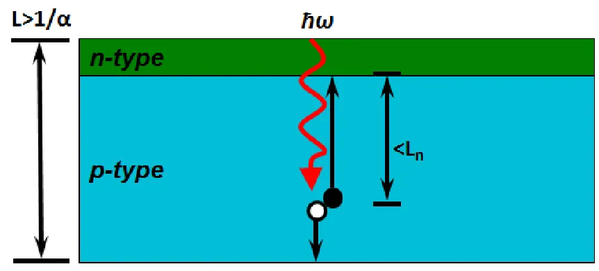
Despite a gradual but consistent decrease in the cost per kilowatt-hour of electricity gener-ated by PVs, [18] the cost is still too high for widespread adoption of this technology. We have been motivated by the potential for radical redesign of the geometry of the PV cell to allow for the use of much lower quality material while retaining reasonable efficiencies, and therefore sharply reducing the cost per kilowatt-hour of PV electricity. Inexpensive candidate materials for use in PV applications generally have either a high level of impu-rities or a high density of defects, resulting in low minority carrier diffusion lengths. [19] Use of such low-diffusion-length material as the absorbing base in a conventional, planar pn junction solar cell geometry (Fig. 1.1) results in devices having carrier collection limited by minority carrier diffusion in the base region. In a solar cell, an incident photon creates an electron-hole pair which is then separated by a built-in electric field. To generate power, the carriers (electrons and holes) must be able to traverse the thickness of the cell. i.e., for a planar solar cell with a p-type base we want:
Ln>1/α (1.5)
and
L >1/α, (1.6)
6
Figure 1.1. Schematic of a traditional planar solar cell design. Shown schematically are the device requirements that when a photon of energy ω generates an electron-hole pair in the p-type base of the cell, the cell thicknessLmust be greater than its optical thickness 1/α, and the minority-electron diffusion lengthLnmust be long enough that any optically-generated minority carrier can reach the pn junction before recombining.
definition, Si has an optical thickness of 125 μm. By employing light-trapping techniques, so that photons pass multiple times through the absorber material before leaving the device, the effective optical thickness of a material is reduced, but equations similar to those above will still apply. This sets a lower limit on the diffusion length that is acceptable for making high-efficiency solar cells from a given material in a traditional, planar pn junction geometry, and thus a lower limit on the material quality and materials costs in fabricating a high-efficiency solar cell. Given the limits to the extent to which light trapping can reduce the need for optically-thick material, [20] [21] [22] materials with diffusion lengths that are very low relative to their optical thicknesses cannot readily be incorporated into high energy conversion efficiency planar solar cell structures.
8
concept of vertical junctions (parallel to incident light) rather than the conventional single horizontal junction (normal to incident light). The merit of such a device lies in the fact that many junctions vertically configured will enable photon-generated minority carriers to have a higher probability of reaching a junction thus increasing carrier collection efficiency and tolerance to radiation damage” (Fig. 1.2). At that time, the goal of the research was to engineer PV devices that were resistant to radiation damage, which is important for deploy-ment in space, to power satellites for example. After a considerable amount of theoretical as well as experimental work in this area, including the demonstration of 15% efficient devices (see, for example, Ref. [26]), the field eventually died out as GaAs became the material of choice for space applications.
10
1.4
Nanowires and Vapor-Liquid-Solid Growth
Nanowires are ubiquitous in the scientific literature, and at the time of writing are being explored by many groups, for example, as potential building blocks for future microelec-tronic circuits as the demands on device size become ever-more demanding. They have also been used as a convenient structure with which to test the properties of very small objects such as quantum confinement and novel transport properties.
Because of these and many other applications, there is a similarly large body of litera-ture on the many different methods of growing nanowires. The Vapor-Liquid-Solid (VLS) technique was first described by Wagner and Ellis in 1964 as a method for growing semicon-ductor “whiskers”. [32] It quickly established itself as a convenient method for producing well-controlled nano- and microwires (where the latter is used to denote wire-like structures with diameters larger than 1 μm) of well-controlled dimensions and orientation, at rapid growth rates. It also has the interesting property that defects tend to be expelled out of the growing crystal, allowing for the growth of single-crystalline material. It is also notewor-thy due to the wide variety of semiconductors and metals that can be grown via the same technique. [33]
In this method of wire growth, semiconductor atoms are introduced in the vapor phase over another semiconductor surface decorated with metal catalyst particles at elevated tem-perature. If the temperature is above the eutectic temperature of the metal-semiconductor alloy, the catalyst particle can act as a sink for semiconductor atoms. As the metal cata-lyst dissolves more and more of the semiconductor, it eventually becomes supersaturated, at which point solid semiconductor is “frozen” out of the alloy. As the gas continues to impinge on the catalyst, the semiconductor grows in one dimension only, in a direction determined by epitaxy with the substrate crystal orientation.
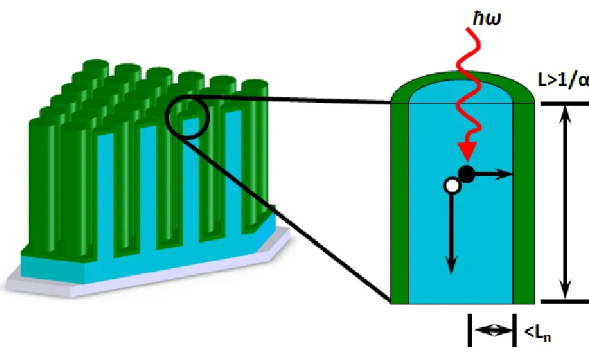
Figure 1.4. Schematic of the radial pn junction, wire array solar cell design (image credit: M. D. Kelzenberg). Shown schematically are the device requirements that when a photon of energy ω generates an electron-hole pair in the p-type core of a wire, the cell thickness (= wire length) L must be greater than its optical thickness 1/α, but that low minority-electron diffusion lengths Lncan be tolerated simply by tuning the wire radius so that any optically-generating minority carrier is within a diffusion length of the pn junction.
deposition (LPCVD) systems, which allowed for much lower processing temperatures (∼ 500◦C rather than∼1000◦C), and also allowed for smaller-diameter wires to be grown. [39] SiCl4 did not disappear completely however, and it has been shown recently that the HCl that is formed in-situ when growing from SiCl4 may make for much easier epitaxy than is possible with SiH4 without significant effort. [40]
1.5
The Radial pn Junction, Wire Array Solar Cell
12
Chapter 2
Solar Cell Device Physics and the Radial
Geometry
2.1
Introduction
In this chapter we will begin by providing motivation for the radial pn junction geometry, and follow with a detailed theoretical comparison of the performance of a PV device with a radial junction vs. one with a planar junction. The chapter concludes with a discussion of similar cylindrical structures with axial, rather than radial, pn junctions.
2.2
“To First Order”: Salient Features
Solar cell efficiency, η, is defined as the ratio of electrical power out (at an operating con-dition of maximum power output), Pout, divided by total optical power in, Pin, typically under AM1.5G1 illumination [43] (see Fig. 2.1) at an intensity of 0.1 W/cm2, i.e.,
η = Pout
Pin (2.1)
= Voc×Jsc×F F
Pin , (2.2)
where the open-circuit voltage Voc is the voltage or bias across the cell when no current is flowing, the short-circuit current densityJsc is the current density at zero bias, and the fill 1AM1.5G stands for Air Mass 1.5, Global illumination. “Air Mass 1.5” indicates that the sunlight has been
attenuated by passage through the Earth’s atmosphere a distance equal to 1.5 times the shortest path (which
is when the sun is directly overhead). “Global” indicates that both direct and diffuse components of sunlight
are included, “AM1.5D”, where the D stands for “Direct” would indicate that only direct illumination is
14
factorF F is the ratio of the maximum electrical power output to the product ofVocandJsc. As minority carrier diffusion length decreases, planar solar cell geometries lose efficiency due to losses in Jsc, Voc and F F. Considering a solar cell as an ideal diode in parallel with a pure light-generated current source leads to the following expression for current generation in a planar pn junction solar cell: [44]
J =Jsc−J0 exp qV kBT −1 . (2.3)
This in turn leads to the following expression for Voc:
Voc= kBT
q ln Jsc J0 + 1 (2.4) ≈ kBT q ln Jsc J0 , (2.5)
whereq= 1.602193×10⁻¹⁹C is the magnitude of the electronic charge,kB= 1.38073×10⁻²³ m2 kg s−2 K−1 is Boltzmann’s constant, and the temperatureT is assumed to be 300 K.
For the purposes of this section, we will treat the minority carrier diffusion length, Ln
(orLp for holes), as the sole metric by which material quality is judged. This quantity is a measure of the average distance a carrier can move from the point of its generation before it recombines. Diffusion length is related to carrier mobility and lifetime by the following expressions: [45]
Ln=Dnτn (2.6)
=
kBT
q μnτn, (2.7)
with similar expressions in the case of holes. As will be discussed in more detail below, for recombination processes dominated by recombination through mid-gap traps (“Shockley Read Hall” recombination [46] [47]), the minority carrier lifetime can also be related to trap density: [45]
τn0= σnNrvth1 , (2.8)
Figure 2.1. The AM 1.5 global (AM 1.5G) spectrum. [43]
Jsc can be considered a measure of the number of light-generated carriers that are swept across the pn junction per unit time, assuming ideal majority carrier transport and collection. We expect thatJsc will increase asLn increases, until some limiting value, when either Ln becomes much larger than the cell thickness, or much larger than the “optical thickness” of the material.
Optical thickness denotes the thickness of material required to absorb all of the above-bandgap photons. Absorption is described by Beer’s Law, which states that light is atten-uated exponentially as a function of material thickness, at each wavelength. The strength of absorption, as a function of wavelength, is given by a material’s absorption coefficient
16 material of thicknessL is
Γ(L) =
dλΓ0(λ)e−L/α(λ). (2.9) Therefore, the total absorption of a piece of material of thicknessL, neglecting all reflection effects, is
Abs(L) = Γ(0)−Γ(L) =
dλΓ0(λ) 1−e−L/α(λ)
. (2.10)
It is tempting to define a wavelength-independent optical constant, say α, to define a wavelength-independent exponential attenuation of light into the semiconductor, i.e., such that
Abs(L)≈
dλΓ0(λ) 1−e−L/α
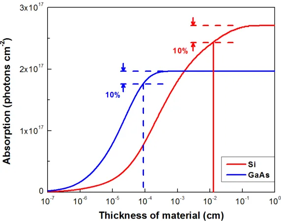
= 1−e−L/α dλΓ0(λ). (2.11) This is, however, impossible, as displayed in Fig. 2.2, where the expressions 2.10 and 2.11 are compared. We therefore define the “optical thickness” of a material to be that thick-ness required to absorb 90% of the above-band-gap photons, and give this the loose desig-nation “1/α”, with the understanding that this does not imply that a single, wavelength-independent, absorption coefficient can adequately describe light absorption in the material. This thickness is 125 μm for Si and is only 891 nm for GaAs (Fig. 2.3).
In the next few paragraphs we will motivate the potential benefits of a radial pn junction geometry with an intuitive model to describe the effects of reducing diffusion length in PV devices. Assume that we have an “optically-thick” (i.e., 125 μm thick) Si PV device with a p-type base, a negligibly thin emitter, insignificant surface recombination, and baseline parameters of the record Si solar cell (the UNSW PERL cell [13]), namelyVoc= 0.706 V,Jsc
= 0.0422 A/cm2, and F F = 0.828, so that η = 24.7%. This means that J0 ≈5.8×10⁻¹⁴ A/cm2 , from Eq. 2.3. Then consider the effect of reducing minority electron diffusion lengthLn. Assume that carrier generation per unit volume is independent of depth into the cell (this is an oversimplification, with a more realistic description given above), and that all carriers generated withinLn of the pn junction are collected, while the rest are not (this is also an oversimplification, with a more realistic treatment given in the next section). i.e., For a planar geometry, assume that
Jsc = 0.0422×Ln
L , Ln≤L (2.12)
18
125 μm) is the cell thickness. Then we can calculate Vocfrom Eq. 2.5, and η from Eq. 2.1, assuming that F F is unaffected by changes inLn.
In the radial pn junction geometry, assume that we again have a 125 μm thick device, this time in the shape of a cylinder, with an emitter layer on the top surface as well as on the side walls. Assume that the cylinder radius is set equal to the minority electron diffusion length Ln, so that, with the additional assumption that all carriers generated within Ln
of the pn junction are collected, Jsc is independent of Ln. Voc can then be calculated by assuming that J0 scales with pn junction area, i.e., that
Voc= kBT
q ln
Jsc J0γ
+ 1
, (2.13)
whereγ is the area of the junction in the cylindrical geometry relative to the area of the top surface of the cylinder (see, for example, [49]). Again, efficiency η can then be calculated from Eq. 2.1. The results of this simple comparison between what we might hope to expect in both geometries are given in Table 2.1.
Table 2.1. Comparison of the basic features of the planar and radial geometries
Ln (μm) 125 100 10 1
Planar cell Jsc (A/cm2) 0.0422 0.0338 0.00338 0.000338
Voc (V) 0.706 0.700 0.641 0.581
FF 0.828 0.828 0.828 0.828
Efficiency (%) 24.7 19.6 1.8 0.2
Radial junction cell Junction Area Increase 3 3.5 26 251
Jsc (A/cm2) 0.0422 0.0422 0.0422 0.0422
Voc (V) 0.678 0.674 0.622 0.563
FF 0.828 0.828 0.828 0.828
Efficiency (%) 23.7 23.5 21.7 19.7
20
in a planar geometry. In reality, carrier generation is highly non-uniform through the cell thickness and occurs much more strongly at the top of the cell, i.e., close to the pn junc-tion. As stated above, in reality light is attenuated exponentially with material thickness, at each wavelength, with shorter wavelengths being absorbed most strongly. Furthermore, the model used above, that collection is guaranteed for carriers within a diffusion length of the junction, and zero for those further away, is not accurate either. Fill factor is also affected by changes in diffusion lengths, and no attempt was made to consider this in the above. Also, we have ignored any issues associated with the inevitably less-than-100 % packing fraction that we will have in the radial geometry (close-packed cylinders can fill at mostπ/(2√3)≈90 % of space) - this may have the effect of reducing theJsc in the radial case although the details are far from trivial. Finally, we have neglected to treat the effects of the emitter, the wire surfaces, and the pn junction region, and the latter especially will prove to be extremely important as we shall see.
Nevertheless, this simple analysis does point to some of the key features we expect to see in the novel geometry. The radial junction is expected to exhibit a much higher tolerance to reduced diffusion lengths than the planar geometry, due to its ability to retain high carrier collection independent of diffusion length. This is paid for by a loss inVoc as junction area increases, but because this is a logarithmic dependence it is a lesser effect. In the planar geometry we expect large losses in Jsc as Ln decreases, and that this will also affect Voc, leading to intolerable losses in efficiency at low (10 μm for Si) diffusion lengths.
2.3
Transport Equations in the Radial Geometry
In order to gain a quantitative understanding of how the radial junction geometry should perform relative to a planar geometry, it is necessary to solve the carrier transport equa-tions in a cylindrical coordinate system. A model for the radial pn junction solar cell was constructed by extending the analysis of the planar cell geometry [44] to a cylindrical ge-ometry. The cell was divided schematically into four regions: the quasineutral part of the n-type emitter region (of width x1), the depletion region of the n-type material (of width
x2), the depletion region of the p-type material (of width x3), and the quasineutral part of the p-type base region (of width xd) (Fig. 2.4).
approxima-Figure 2.4. Generalized band structure for a pn heterojunction structure. Shown are the conduction and valence band energies, Ec and Ev, as well as the equilibrium Fermi energy
[image:37.612.166.480.183.438.2]22
tion was invoked. The emitter layer (i.e., the exterior “shell” of the wire) was assumed to be n-type, while the base (i.e., the interior “core” of the wire) was assumed to be p-type (see Fig. 2.5. The analogous schematic for the planar structure is shown in Fig. 2.6). Light was assumed to be normally incident on the top face of the wire, with no reflection losses. Re-combination was assumed to be purely due to the Shockley-Read-Hall reRe-combination from a single trap level at midgap; [47] other recombination processes, such as Auger recombi-nation, were neglected. However, surface recombination effects were included, by assuming a minority carrier surface recombination velocityS at ther = R surface.
To simplify the analysis and to allow for analytic solutions, the minority carrier trans-port in the wire structure was assumed to be purely radial. The approximation of one-dimensional carrier transport is valid when the variation in carrier concentration in the z
direction occurs over a much longer length scale than that in the r direction. This is an appropriate assumption for a radial pn junction wire in a material that is collection limited, that is, one with an optical thickness (see Ch. 2.2) that is much greater than the diffusion length of minority carriers. In this case, the variation in carrier concentration in the axial direction is primarily due to light absorbtion and occurs over a large distance relative to the variation in carrier concentration in the radial direction, which occurs due to diffusion and drift resulting from the potential drop at the pn junction interface.
Although individual wires may have a high resistance, the IR drop in a wire can still be very low because of the very small current that will pass through each wire. Given a resistivity ∼10−2 Ω cm (appropriate for Si with doping ∼1018 cm−3), [50] a wire length ∼ 100 μm, and a current density ∼ 0.05 A cm−2, the IR drop in a wire due to series resistance is∼10−5 V. Hence, it was reasonable to assume, as we did, that the exterior of the wire was an equipotential surface relative to the core of the wire.
The total photogenerated carrier flux was calculated by an integration that is equivalent to summing up the contributions at each value of z at a given bias, and the dark current was calculated for the entire junction area neglecting the ends. The bias was then varied, creating a current-density versus voltage (J−V) curve (not shown), from which the open-circuit voltage, short-open-circuit current density, fill factor, and efficiency could be calculated.
24
Figure 2.6. A conventional planar solar cell is a pn junction device. Light is incident on the top surface. The top surface (“emitter”) is n-type, the base is p-type. Ec is the conduction band energy,Evis the valence band energy, andEf is the Fermi energy. The n-type material has thicknessd1; the p-type material has thicknessd2. The total cell thicknessL=d1+d2. Recombination at the sidewalls is neglected; i.e., it is assumed that lateral dimension of the cell is much greater than its vertical thicknessL - the aspect ratio of the cell is greatly exaggerated in this schematic.
normal incidence, light that is incident on the top of a wire will remain within the wire due to total internal reflection, while light that is not incident on the top of a wire may pass through many rods while traversing the cell due to the high-aspect ratio of the wires. The details await further study.
2.3.1 Quasineutral Regions
In analogy to treatments of planar pn junctions, [44] the minority-carrier movement in the quasineutral region of the p-type base (i.e. core) material was assumed to be governed by the transport equation,
∇2n− n
Ln2 = ∂2n
∂r2 +
1
r ∂n
∂r − n Ln2 =−
α2Γ0
Dn e α2z
, (2.14)
diffusion coefficient. The boundary conditions are
n(0) = finite, (2.15)
n(x4) = n0
eqV /kBT −1
, (2.16)
where V is the applied bias, and the temperatureT is assumed to be 300 K. The current density in the p-type quasineutral region,Jp, is thus
Jp = 2x4 L
0 Jp(z)dz
R2 , (2.17)
where
Jp(z) =−qDn ∂n
∂r
r=x4
, (2.18)
and R and Lare the radius and length of the wire, respectively.
In the quasineutral region of the n-type emitter, the transport equation is
∂2p ∂r2 +
1
r ∂p
∂r − p Lp2 =−
α1Γ0
Dp e α1z
, (2.19)
wherep =p−p0 is the excess minority-hole concentration with respect to the equilibrium valuep0 ,Lp is the diffusion length of minority holes, α1 is the absorption coefficient of the n-type material, andDp is the minority-hole diffusion coefficient. The boundary conditions were
p(R−x1) = p0
eqV /kBT −1
, (2.20)
Spp(R) = −Dp ∂p
∂r
r=R
, (2.21)
where Sp is the surface-recombination velocity of holes at the external surface of the wire. Hence, the current density in the n-type quasineutral region,Jn, is
Jn= 2(R−x1) L
0 Jn(z)dz
R2 , (2.22)
where
Jn(z) =qDp ∂p
∂r
r=R−x1
26 2.3.2 Depletion Region
The depletion region width was obtained by solving Poisson’s equation in the depletion region, assuming that the electric fieldE was zero outside of the depletion region, thatE
was continuous across the junction, whereis the dielectric constant of the semiconductor, and that ionized donors and acceptors were the sole constituents of charge (i.e. the depletion approximation was invoked).
The light-generated current density in the depletion region, Jgdep, was calculated by
assuming that all incident light that was absorbed produced carriers that were collected, which is reasonable given the strength of the electric field within this region. Hence, in the p-type part of the depletion region
Jgdep,p(V) =qΓ0
1−e−α2L d22−x42
R2 , (2.24)
whereas in the n-type part of the depletion region
Jgdep,n(V) =qΓ0
1−e−α1L(d2+x2)2−d22
R2 . (2.25)
The recombination current density in the depletion region was approximated by assum-ing that the potential in the depletion region was a linear function ofr. The recombination current density for the entire depletion region was calculated by multiplying the maximum recombination rate by a small volume centered about this maximum recombination point, in analogy with the standard treatment of the planar case. [51]
2.3.3 Solution
Solving the above equations with the stated assumptions produced the following expression for theJ-V behavior of the device:
J = (J0p+J0n)
eqV /kBT −1
−Jlp−J n
l +Jrdep(V)−Jgdep,p(V)−Jgdep,n(V), (2.26)
J0p =−2qn0LDn
Lp2 β5
β12
I1(β5)
I0(β5), (2.27)
J0n=−2qp0LDp
Lp2 β2
β12
f1K1(β2)−f2I1(β2)
f1K0(β2) +f2I0(β2)
, (2.28)
Jlp =−2qΓ0Ln 2
Lp2 β5
β12
I1(β5)
I0(β5)
1−e−β6, (2.29)
Jln=−2qΓ0 β2
β12
K1(β2) (f1−β4I0(β2))−I1(β2) (f2+β4K0(β2))
f1K0(β2) +f2I0(β2)
×1−e−β3, (2.30)
Jgdep,p(V) =−qΓ0
d22−x42
R2
1−e−β6, (2.31)
Jgdep,n(V) =−qΓ0
(d2+x2)2−d22
R2
1−e−β3, (2.32)
Jrdep(V) =−qLUmax
r22−r12
R2 , (2.33)
where In(x) andKn(x), n= 0 or 1, represent modified Bessel’s functions of the first and second kinds, respectively.
The dimensionless parameters are defined as
β1=R
Lp, (2.34)
β2=R−x1
Lp , (2.35)
β3=α1L, (2.36)
β4=LpSp
Dp , (2.37)
β5=x4
Ln, (2.38)
β6=α2L, (2.39)
f1=f1(β1, β4)
=I1(β1) +β4I0(β1), (2.40)
f2=f2(β1, β4)
28 Additionally,
Umax =√ni,∗
τn0τp0sinh
qV
2kBT
. (2.42)
r1(V) =r(V)−(x2(V) +x3(V))
2 κ, (2.43)
r2(V) =r(V) +(x2(V) +2 x3(V))κ, (2.44)
r(V) =x4+ log Na ni,p log
NaNd
ni,pni,n
(x2(V) +x3(V)), (2.45)
κ= πkBT
q(Vbi−V), (2.46)
Vbi−V =qNd
2n (d2+x2)
2logd2+x2
d2
+qNd 4n d2
2+ (d
2+x2)2
+qNa 2p x4
2logx4
d2
+qNa 4p
d22−x42, (2.47)
whereNa,ni,p,p, andτn0are the dopant (acceptor) density, intrinsic carrier concentration, dielectric constant, and lifetime in the depletion region, respectively, for the p-type material.
Nd,ni,n,n, andτp0are the analogous quantities for the n-type material. Also,ni,∗=ni,por
ni,n, depending on whether the maximum recombination point lies in the p-type or n-type material. From Eq. (2.47), x2(V) and x3(V) can be found numerically, given the built-in voltage Vbi:
Vbi= kBT
q log
NaNd ni,pni,n
+ΔEc
q , (2.48)
where ΔEc is the conduction-band offset (= 0 for homojunctions).
2.4
Numerical Assessment of Device Behavior in Si
for Si and GaAs. [48] The current densityJ was calculated by numerically integrating over wavelength, at each value of the forward bias V, to obtain a value for the total current density as a function of bias.
Two regimes were treated - (1) the trap density in the quasineutral region was assumed to be independent of the trap density in the depletion region, with the trap density in the depletion region set at a low level such that depletion region traps had negligible effect on cell performance, and (2) the trap density was assumed constant through the material, and thus the minority-carrier lifetimes in the quasineutral region and in the depletion region were identical. For a solid-state device the latter scenario is likely to be more realistic, but treating the two cases separately allowed us to gain insight into the different regimes of cell performance. Also, depending on the specific fabrication process used to make the radial pn junction cell, the former regime may also be realizable. The lifetimes in the depletion region are given by [45]
τn0 = 1
σnNrvth, (2.49)
τp0 =σpNrvth1 , (2.50)
whereσn andσp are the cross sections for electron and hole capture, respectively,Nr is the density of recombination centers, and vth is the thermal velocity. To first order, σn =σp, so that τn0=τp0.
In case (2), the high doping levels we considered (1018 cm−3) implies that [47]
τn≈τn0, (2.51)
τp≈τp0, (2.52)
so that τn = τp = τn0 = τp0, where τn is the lifetime of minority electrons in the p-type quasineutral region, andτpis the lifetime of minority holes in the n-type quasineutral region. In turn, these lifetime values yield values forLn and Lp through the relations [45]
Ln=τnDn, (2.53)
30 where
Dn,p= kBT
q μn,p. (2.55)
Hence, given values for μn and μp, [52] in this case only one parameter, i.e. τn, needs to be specified to determine the values ofτn,τp,τn0,τp0,Ln, and Lp.
In case (1), the assumption that τn =τp and τn0 =τp0 was retained, butτn0 was held fixed (at 1 μs, or, equivalently, trap density Nr was held fixed at 1014 cm−3, while τn was allowed to vary independently. Then the above relations were used to relate Ln and Lp
to τn. This set of conditions simulated the situation in which the impurity profile was not constant throughout the sample. Case (1) led to quasineutral region recombination always being the dominant recombination mechanism, while in case (2) quasineutral region recombination dominated for τn 40 ns, with depletion region recombination dominating for shorter lifetimes.
2.4.1 Preliminary Observations
The behavior of the cells was first investigated as a function of doping levels in the emitter and base, emitter thickness, and wire radius. Some general conditions for an optimal cell thus became apparent. At a given value of the minority-electron diffusion length, radial junction cells favored high doping. Furthermore, smaller wire radii necessitated high doping to prevent full depletion of the wire core. Carrier mobility is coupled to the doping in a well known fashion in Si, [52] the lifetime is related to the trap density in (2.49) and (2.50) above, and the mobility, lifetime, and diffusion length are related in (2.53)-(2.55). At a fixed trap density, increasing the doping will decrease the mobility and hence decrease the diffusion length. On the other hand, increasing the doping level will increase the built-in voltage, through (2.48). And because carriers travel a mean distance of one diffusion length through a quasineutral region before recombining, setting the wire radius approximately equal to the minority-electron diffusion length allows carriers to traverse the cell radially even if the diffusion length is low, provided that the trap density is relatively low in the depletion region.
length of the wire became much greater than the optical thickness of the material. Also,Jsc
was essentially independent of wire radius, provided that the radius was less thanLn. The value ofJsc decreased steeply for R > Ln. Jsc was essentially independent of trap density in the depletion region.
The open circuit voltage Voc decreased with increasing wire length, and increased with increasing wire radius. The extent to which Voc decreased with increasing wire length depended strongly on the trap density in the depletion region: as the trap density became high (>∼3×1015 cm−3 for Si) in the depletion region, theVoc declined rapidly. The trap density in the quasineutral regions, on the other hand, had relatively less effect on Voc.
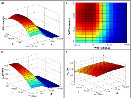
We can thus identify two regimes. In the regime of low depletion region trap density (3× 1015 cm−3 for Si), in which quasineutral region recombination dominates depletion region recombination, Voc is lost through the geometric increase in pn junction interface area γ, and the subsequent decrease in light-generated current relative to dark current, per unit junction area, as described above in Ch. 2.2, as well as in [49]. In the regime in which depletion region recombination dominates (Nr 3×1015 cm−3 for Si), the high trap density effectively greatly increases the dark current, in addition to the geometrical effects. The optimal wire dimensions are obtained when the wire radiusR is between about 0.5 and 1 times the minority carrier diffusion length in the core of the wires (Ln for a p-type core) and a length that is determined by the specific trade-off between the increase in Jsc
and the decrease in Voc with length (Figs. 2.7, 2.8, and 2.9). If the trap density in the depletion region is relatively low (i.e., <∼3×1015 cm−3 for Si), the maximum efficiency occurs for wires having a length approximately equal to the optical thickness (∼ 125 μm for Si). For higher trap densities in the depletion region, shorter wire lengths are optimal.
Because majority carrier transport issues are neglected, this model shows that in the planar case the efficiency reaches a limiting value as the thickness increases. In contrast, the efficiency of the radial pn junction cell attains a maximum as a function of thickness - if the thickness is increased further, the efficiency is reduced. This behavior can be understood by realizing that the light-generated current density goes as
Jl∼(1−e−αL), (2.56)
32
34
current density goes as
J0 ∼L. (2.57)
The competition between these two effects determines the optimum thickness of the radial pn junction cell for maximum energy conversion efficiency.
2.4.2 Simulation Parameters
Given these observations, a comparison of the radial and planar junction geometries was undertaken in Si with the following parameters. An n+ / p+ structure was assumed, with the top layer and the external shell (the emitter) being n+ in the planar and radial junction cells, respectively. The wire radius was set equal to the minority electron diffusion length
Ln, a condition that was found to be near-optimal in all cases. In many cases the optimal radius was in fact less than Ln (with the optimal value tending to fall between 0.5 and 1 times the minority carrier diffusion length), but the difference in performance as R was varied in this range was small for our purposes (usually less than 0.5% absolute, whereas if
Rwas increased significantly aboveLnthe drop in performance was much more significant). A fixed ratio between Ln and R simplified the analysis while allowing us to examine key features of the design. Other parameters were set as follows:
Nd=1×1018 cm−3, Na=1×1018 cm−3, μp =95 cm2 V−1 s−1,
⇒Dp =kBT
q μp = 2.46 cm
2 s−1,
μn=270 cm2 V−1 s−1,
⇒Dn=kBT
q μn= 6.98 cm
2 s−1,
d1 =x1+x2 ≥1×10⁻⁶ cm, Sp =Sn= 1×105 cm s−1, σp =σn= 1×10⁻¹⁵ cm2,
36
Figure 2.10. Short-circuit current density Jsc vs. cell thickness L and quasineutral region minority-electron diffusion length Ln for (a) a conventional planar pn junction Si cell and (b) a radial pn junction Si cell. In both cases the short-circuit current density is unaffected by decreasing the trap density in the depletion region. In the radial pn junction case, the cell radiusR is set equal toLn, a condition that was found to be near optimal.
where the ≥ symbol indicates that d1 was set equal to 1 × 10⁻⁶ cm, unless this was too small to allow the full voltage dropVbi to occur across the pn junction. In the latter case,
d1 was set equal to the minimum value required to achieve a voltage drop Vbi. The model assumes that the materials are not doped so heavily as to become degenerate; [45] also, the model does not account for Auger recombination. [53] Since these effects both become significant at higher dopings levels, the doping was not set to an even higher value.
2.4.3 Quasineutral Region Recombination Dominated Analysis
In the first analysis, the trap density in the quasineutral region was assumed to be inde-pendent of the trap density in the depletion region, with the trap density in the depletion region set at a low level (1014cm−3), such that depletion region recombination was included but had negligible effect on cell performance. This led to quasineutral region recombination dominated loss mechanisms at all parameters considered.
Figure 2.11. Open-circuit voltageVoc vs. cell thicknessLand quasineutral region minority-electron diffusion length Ln for (a) a conventional planar pn junction Si cell and (b) a radial pn junction Si cell. Depletion region trap density is held fixed at a relatively low level, Nr= 1014cm−3, so that depletion region lifetimeτn0 = 1 μs, leading to quasineutral region dominated recombination. In the radial pn junction case, the cell radius R is set equal toLn, a condition that was found to be near optimal.
to ≈35 mA/cm2 as the wire radius increased above 1μm, whereas in the planar geometry
Jsc dropped from 34 to 4 mA/cm2 asτn decreased from 14μs to 14 ps (so that Lndropped from 100 μm to 100 nm in the quasineutral region of the p-type material). Note that a Si cell of thickness L = 100 μm is not optically thick, in that it absorbs less than 90% of the incident photons with energy above the bandgap (see 2.2 above). Jsc approached ∼43 mA/cm2 in both geometries as Ln approached 1 mm, in the limit of large L (> 1 mm). The radial pn junction design overcomes the problems of carrier collection that are present in the conventional planar geometry.
38
Figure 2.12. Fill factor F F vs. cell thicknessL and quasineutral region minority-electron diffusion length Ln for (a) a conventional planar pn junction Si cell and (b) a radial pn junction Si cell. Depletion region trap density is held fixed at a relatively low level,Nr= 1014 cm−3, so that depletion region lifetimeτn0= 1μs, leading to quasineutral region dominated recombination. In the radial pn junction case, the cell radiusRis set equal toLn, a condition that was found to be near optimal.
the depletion region was held fixed at 1μs. In the planar geometry the open-circuit voltage dropped from 0.59 to 0.49 V over the same range.
The fill factor was nearly constant at ∼0.8 as a function of L and Ln for both planar and radial geometries in this regime, reaching a maximum of∼0.84 within the range ofL,
R, andLnconsidered (Fig. 2.12).
Taken together, the factors discussed above meant that the efficiency of the radial pn junction solar cell remained high despite a high quasineutral-region trap density (Fig. 2.13). In the planar geometry, a high quasineutral-region trap density led to a very lowJsc. This behavior inevitably results in a low efficiency for such systems (Fig. 2.13(a)). In contrast, for the radial pn junction, Jsc can attain high values even for very large trap densities in the quasineutral regions. Voc, and thus the overall efficiency, can remain high.
Figure 2.13. Efficiency η vs. cell thickness L and quasineutral region minority-electron diffusion length Ln for (a) a conventional planar pn junction Si cell and (b) a radial pn junction Si cell. Depletion region trap density is held fixed at a relatively low level,Nr= 1014 cm−3, so that depletion region lifetimeτn0= 1μs, leading to quasineutral region dominated recombination. In the radial pn junction case, the cell radiusRis set equal toLn, a condition that was found to be near optimal.
that τn ≈ 1.4 ns) in the quasineutral regions and τn0 = 1 μs in the depletion region, the maximal efficiency of the radial pn junction geometry was 13%, compared with 5% in the planar geometry. This maximal efficiency occurred for a radial pn junction cell between 100 and 240 μm thick, whereas the efficiency saturated in the planar geometry when thickness exceeded 5μm.
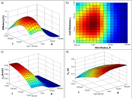
2.4.4 Homogeneous Trap Distribution Analysis
The situation was also analyzed in the case thatτn0=τp0=τn=τp, so that the trap density was assumed constant through the material. In this case, quasineutral region recombination was the dominant loss mechanism only until some critical value of depletion region trap density (or, equivalently, ofτn0 andτp0), and for trap densities above this, depletion region recombination began to dominate.
The results forJscare shown above in Fig. 2.10. These results, for both planar and radial pn junction cells, were unaffected by changing the trap density in the depletion region.
40
Figure 2.14. Open-circuit voltageVoc vs. cell thicknessLand quasineutral region minority-electron diffusion length Ln for (a) a conventional planar pn junction Si cell and (b) a radial pn junction Si cell. Depletion region trap density is set equal to quasineutral region recombination density, leading to depletion region dominated recombination at low values of Ln. In the radial pn junction case, the cell radiusR is set equal to Ln, a condition that was found to be near optimal.
case (Fig. 2.14). In the planar case, the open-circuit voltage is independent of cell thickness and decreases as the quasineutral region electro
![Figure 1.3.Schematic of the Parallel Multjunction (PMJ) solar cell design (after [27]).](https://thumb-us.123doks.com/thumbv2/123dok_us/309255.1032156/25.612.112.540.140.424/figure-schematic-parallel-multjunction-pmj-solar-cell-design.webp)
![Figure 2.1. The AM 1.5 global (AM 1.5G) spectrum. [43]](https://thumb-us.123doks.com/thumbv2/123dok_us/309255.1032156/31.612.133.499.119.431/figure-the-am-global-am-g-spectrum.webp)