http://dx.doi.org/10.4236/jemaa.2015.72004
Grating Lobe Suppression with Element
Count Optimization in Planar Antenna Array
B. Rama Sanjeeva Reddy, D. Vakula
Department of Electronics and Communication, National Institute of Technology, Warangal, India Email: [email protected], [email protected]
Received 6 February 2015; accepted 24 February 2015; published 26 February 2015
Copyright © 2015 by authors and Scientific Research Publishing Inc.
This work is licensed under the Creative Commons Attribution International License (CC BY). http://creativecommons.org/licenses/by/4.0/
Abstract
The novel approach of this paper describes the suppression of grating lobe level with the element count optimization in planar antenna array. Rectangular lattice (RL) and triangular lattice (TL) structures are chosen for determining the achievable array element patterns (EP) and further suppressing the grating lobe level. The element spacing and number of elements (10 × 20 array) are taken into account for particular lattice. Grating lobe peaks are observed for the 200-element planar array at maximum scan angle (θ) with the set frequency of 3 GHz. Further, it is found that 14˚ bore sight elevation of rectangular lattice produces a transformed field of view, which permits a reduction in element count of 20.39% compared with 10˚ bore sight elevation. Finally, the typi-cal values of elevation, element count and array size (25 cm2) are trained using artificial neural
network (ANN) algorithm and element count is predicted after testing the network. The network shows a high success rate.
Keywords
Rectangular Lattice (RL), Triangular Lattice (TL), Element Pattern (EP), Artificial Neural Network (ANN)
1. Introduction
re-sults when array elements located in close proximity interact in a manner that alters the element count and ele-ment patterns.
Because of the difficulty associated with predicting these effects, grating lobe level is traditionally considered an obstacle to array design. Grating lobe typically tends to make the active element pattern more directive than the ideal element pattern indicating high scan roll off of the array.
One of the important array design parameters is element spacing. It is often desirable to design a planar array with larger element spacing so that more real estate can be made available for transmission lines and discrete components [2].
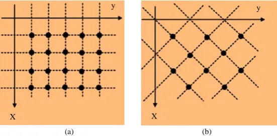
However, to avoid the formation of high grating lobes, element spacing is limited to less than 1λ0 for broad-side beam design and less than 0.6λ0 for a wide-angle scanned beam. In designing a wide-angle scanned planar array, rectangular and triangular lattice structures are taken as shown in Figure 1.
Selection of the maximum element spacing corresponding to the minimum number of controlled elements in the limited-scan arrays results in the presence of the array factor grating lobes in real space [3].
The higher level of lobe is usually undesirable, since it corresponds to lowering the array gain due to taking a part of the radiated power away from the main lobe [3].
The grating lobes of a planar array antenna are conveniently shown in the projection coordinates space as given in Equation (1), by making use of the direction cosines u and v, where
sin cos , sin sin .
u=
θ
ϕ
v=θ
ϕ
(1)The rectangular lattice array with axes parallel to array edges, the incipient grating lobes in the array plane given by Equation (2), determines the optimum lattice spacing is given by [3],
[
]
1
sin L sin .
θ
′ = −λ
+θ
(2)
2. Analysis of Grating Lobes
The grating lobe constraint restricts array element spacing and is a result of the array periodicity. The periodicity imposes constraints on element spacing in order to avoid the formation of unwanted radiation peaks called grat-ing lobes. First gratgrat-ing lobe is parallel to the array when the beam is scanned to an angle
θ
′
off bore sight and the length of the array (L = Nd, N = number of elements and d = inter element spacing). The position of the first outside (array from bore sight) null for an array beam steered to θ and is given as [3],(
1 sin)
d=λ + θ′ (3)
As
θ
′
= 60˚, the separation d can be large as 0.536λ before the grating lobe peak emerges from the plane of the array as defined by Equation (3). For element (k, l), the phase of element relative to (1, 1) element, ψkl is given as,(
)
(
)
0 1 sin cos 0 1 sin sin
kl k k dx k l dy
ψ = − θ ϕ+ − θ ϕ (4)
where k0 = 2π/λ0 and the planar array radiation is given by Equation (5),
X
y
X
y
[image:2.595.175.451.569.705.2](a) (b)
(
)
(
)
0( 1) sin cos 0( )1 sin sin1 1
, , e x y
K L
j k k d k l d
e
k l
S θ ϕ S θ ϕ − θ ϕ+ − θ ϕ
= =
= ⋅
∑∑
(5)(
,)
e
S θ ϕ is array element radiation pattern and the grating lobes occur [4] when
(
1)
y(
1)
x d
d
k u l v m
λ − + λ − = (6)
m is integer number. This condition can only be met if to start with ,
x y
u p v q
d d
λ λ
= = where p & q are integer
numbers.
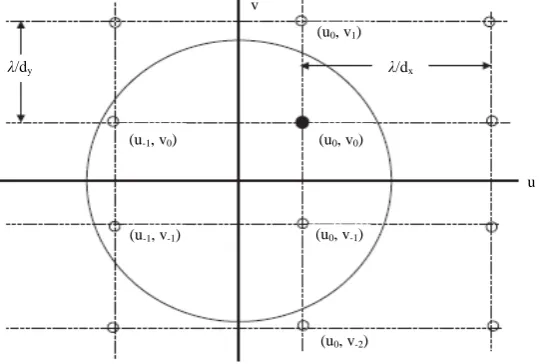
Subject to the condition that, these lobes fall within the unit circle of u2+v2<1. In u-v space, the area with circle of radius “one” corresponding to real angles θ and φ (−90˚ < θ < 90˚, 0˚ < φ < 360˚) and is called visible space as in Equation (6). The area outside this is called invisible space with complex angles. For an element dis-tance equal to one wavelength, grating lobes occur in the principal planes (u = 0, v = 0). Choosing the larger spacing for dy λ and with v = 0, generates a lobe (u0, v−1) as shown inFigure 2.
This often yields unsatisfactory results since grating lobes changes the element performance from the isolated response. The array designer must balance avoiding undesired mutual coupling effects with eliminating grating lobes due to the element spacing at the high end of the frequency band [4] [5]. This limits the array bandwidth when designing with traditional elements.
Elements that are typically used in wideband arrays also tend to be deep and not amenable to conformal ap-plications. These limitations have prevented array designers from providing array systems that are wideband, planar, and free from grating lobes over a large scan volume. The spacing of the array’s elements should be chosen such that grating lobes do not occur when the main beam is steered within the boundaries of the specified field of view [5] [6]. In addition, it is desirable to space the elements as far apart as possible, in the context of the grating lobe constraint, in order to minimize array cost and complexity, since larger separation permit a giv-en aperture to be filled using fewer elemgiv-ents [7].
3. Optimization of Element Count in Planar Arrays
Artificial Neural Network is used for this problem in optimizing the element count taking in to account the grat-ing lobe level for a given array area and variation of bore sight elevation from 10˚ to 40˚ with a step of 2˚.
The ability of these networks to generalize relationships between inputs and outputs is a key to their effec-tiveness [8]. The accuracy of a properly trained network depends on the accuracy of the data used to train the network. Therefore care must be taken while generating training data, whether the data is generated by simula-tion or experimentally [9]. The data patterns generated are well trained and confined in retrieving the actual and
(u-1, v0) (u0, v0)
(u0, v-1)
(u-1, v-1)
(u0, v-2)
u v
(u0, v1)
λ/dx
[image:3.595.177.447.521.703.2]λ/dy
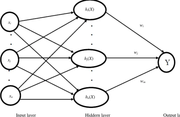
predicted values of both rectangle and triangular lattice structures. The inputs of the network are expressed as vector {X}, hidden layer is represented by h(X) and output layer is denoted by {Y} as represented in Figure 3 [10].
4. Results and Discussion
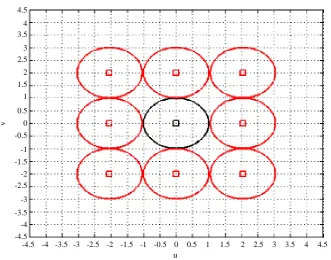
Grating lobe patterns are generated for the case of rectangular lattice planar array antenna structure with element spacing of dx = 0.29λ, dy = 0.5λ as shown inFigure 4.
Input layer Hiddern layer Output layer xn
xj
xi
wi
wj
wm
hn(X)
hj(X)
hi(X)
Figure 3.Artificial neural network structure (radial basis function).
v
u -2.5
0 1
4.5 4 3.5 3 2.5 2 1.5 1 0 0.5 -0.5 -1 -1.5 -2 -2.5 -3 -3.5 -4 -4.5 -4.5
[image:4.595.143.458.188.393.2]-4 -3.5 -3 -1.5 -2 -0.5 -1 0.5 2 1.5 3 2.5 4 3.5 4.5
Figure 4.Grating lobe diagram for rectangular lattice planar array antenna for dx = 0.29λ, dy =
Different values of inter element spacing of planar array elements considered in order to control the grating lobe levels. The patterns are generated for the case of rectangular and triangular lattice structure. Inter element spacing for the rectangular lattice structures are shown in Figures 4-6 and the triangular lattice structures are represented from Figures 7-9.
[image:5.595.149.479.145.399.2]v u -2.5 0 1 4.5 4 3.5 3 2.5 2 1.5 1 0 0.5 -0.5 -1 -1.5 -2 -2.5 -3 -3.5 -4 -4.5 -4.5 -4 -3.5 -3 -1.5 -2 -0.5 -1 0.5 2 1.5 3 2.5 4 3.5 4.5
Figure 5.Grating lobe diagram for rectangular lattice planar array antenna for dx = 0.39λ, dy
= 0.5λ.
v u -2.5 0 1 4.5 4 3.5 3 2.5 2 1.5 1 0 0.5 -0.5 -1 -1.5 -2 -2.5 -3 -3.5 -4 -4.5 -4.5 -4 -3.5 -3 -1.5 -2 -0.5 -1 0.5 2 1.5 3 2.5 4 3.5 4.5
Figure 6. Grating lobe diagram for rectangular lattice planar array antenna for dx = 0.49λ, dy
[image:5.595.145.477.436.696.2]v
u -2.5
0 1
4.5 4 3.5 3 2.5 2 1.5 1 0 0.5 -0.5
-1 -1.5 -2 -2.5 -3 -3.5 -4 -4.5 -4.5
-4 -3.5 -3 -1.5 -2 -0.5
-1 0.5 2 1.5 3 2.5 4 3.5 4.5
Figure 7. Grating lobe diagram for triangular lattice planar array antenna for dx = 0.29λ, dy = 0.5λ.
v
u -2.5
0 1
4.5 4 3.5 3 2.5 2 1.5 1 0 0.5 -0.5
-1 -1.5 -2 -2.5 -3 -3.5 -4 -4.5 -4.5
-4 -3.5 -3 -1.5 -2 -0.5
-1 0.5 2 1.5 3
2.5 4 3.5 4.5
It is observed that with the position change of the grid points in the lattice, the fine tuning of the grating lobes are controlled. Simulations are carried using MATLAB software.
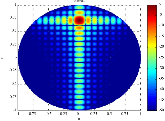
Array element patterns (EP) with normalized (dB) and general values (dB) are also generated for triangular lattice structure and are as shown in Figure 10, Figure 11. Further, the performance of the grating lobes is ex-tended with optimization of element count using ANN.
v
u -2.5
0 1
4.5 4 3.5 3 2.5 2 1.5 1 0 0.5 -0.5 -1 -1.5 -2 -2.5 -3 -3.5 -4 -4.5 -4.5
[image:7.595.145.483.459.706.2]-4 -3.5 -3 -1.5 -2 -0.5 -1 0.5 2 1.5 3 2.5 4 3.5 4.5
Figure 9.Grating lobe diagram for triangular lattice planar array antenna for dx = 0.49λ, dy =
0.5λ.
0
-5
-10
-15
-20
-25
-30
-35
-40
-45
-50 -0.75
v
Pattern
-1
-1 -0.75 -0.25 u -0.5
-0.5 -0.25 0 0.25 0.75
0.5 1
0.25 0.5 0.75 1 0
The optimized element count for triangular array element pattern provides element savings of 13%, 13.2% and 25.03% for 10˚, 14˚ and 26˚ bore sight elevations respectively, relative to the optimum rectangular lattice.
[image:8.595.144.481.184.420.2]The data patterns are well trained and tested further in determining the predicted element count. Table 1 shows the actual and predicted element count values for the inputs selected for the rectangular lattice structure. The network performs high success rate.
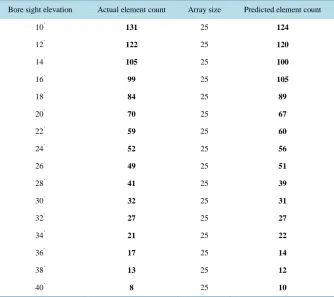
Table 2 shows the actual and predicted element count values for the inputs selected for the triangular lattice structure. The network performs high success rate.
0
-5
-10
-15
-20
-25
-30
-35
-40
-45
-50 -1 -0.75 -0.5
-0.25 0
0.25 0.5 0.75 1
u v -0.75 -1
-0.5 -0.25 0 0.25 0.5 0.75 1 -50 -40 -30 -20 -10 0
d
B
Pattern
[image:8.595.142.480.453.724.2]Figure 11. Total array pattern plot (dB) for 10 × 20 triangular array.
Table 1.Actual and predicted values of optimum element count (rectangular lattice).
Bore sight elevation Actual element count Array size Predicted element count
10˚ 152 25 151
12˚ 139 25 139
14˚ 121 25 119
16˚ 114 25 110
18˚ 102 25 101
20˚ 89 25 87
22˚ 81 25 82
24˚ 74 25 71
26˚ 66 25 64
28˚ 59 25 52
30˚ 54 25 50
32˚ 47 25 48
34˚ 42 25 45
36˚ 34 25 39
38˚ 24 25 22
Table 2. Actual and predicted values of optimum element count (triangular lattice).
Bore sight elevation Actual element count Array size Predicted element count
10˚ 131 25 124
12˚ 122 25 120
14˚ 105 25 100
16˚ 99 25 105
18˚ 84 25 89
20˚ 70 25 67
22˚ 59 25 60
24˚ 52 25 56
26˚ 49 25 51
28˚ 41 25 39
30˚ 32 25 31
32˚ 27 25 27
34˚ 21 25 22
36˚ 17 25 14
38˚ 13 25 12
40˚ 8 25 10
5. Conclusion
An approach of grating lobe suppression with the array element count optimization using neural network is ob-tained. Analysis on the grating lobe and conditions applied for suppression is explained and performed with maximum scan angle. With change in the bore sight elevation value in rectangular and triangular structures, the grating lobes are observed for different inter element spacing using MATLAB simulation. The element count decreases with the increase in bore sight elevation. Comparison of both lattice structures gives the proper opti-mization of element count with the variation in different values of elevation. As observed, the optimum element savings of about 25.03% for 26˚ elevations is achieved for triangular array when compared with optimum rec-tangular array. Element count optimization for grating lobe suppression is obtained using radial basis function ANN. The network shows a high success rate for element count for RL and TL structures.
References
[1] Grillo, G. and Sergei Skobelev, P. (2011) Phased Array Antennas with Optimized Element Patterns. 2nd Edition, Ar-tech House, London.
[2] Denisenko, V.V. (2005) A Multi-Element Phased Antenna Array of the Ka Band. Antenny, 1, 7-14.
[3] Visser, H.J. (2005) Array and Phased Array Antenna Basics. 2nd Edition, John Wiley & Sons Ltd., Hoboken.
http://dx.doi.org/10.1002/0470871199
[4] Huang, C., Zhao, Z., Feng, Q. and Luo, X. (2011) Suppression of Grating Lobes from a Corrugated 2 × 2 Slot Antenna Array with Element Spacing beyond a Wavelength. IET Microwaves, Antennas Propagation, 5, 1607-1612.
http://dx.doi.org/10.1049/iet-map.2010.0575
[5] Toyama, N. (2005) Aperiodic Array Consisting of Sub Arrays for Use in Small Mobile Earth Stations. IEEE Transac-tions on Antennas and Propagation, 53, 2004-2010. http://dx.doi.org/10.1109/TAP.2005.848486
[6] Chang, K. (2005) Encyclopedia of RF and Microwave Engineering. Vol. 6, 252-254.
http://dx.doi.org/10.1002/0471654507
[8] Patnaik, A., Anagnostou, D.E. and Christodoulou, C.G. (2004) Applications of Neural Networks in Wireless Commu-nications. IEEE Antennas and Propagation Magazine, 46, 130-137. http://dx.doi.org/10.1109/MAP.2004.1374125
[9] Bregains, J.C., Dorado, J., Gestal, M., Rodriguez, J.A., Ares, F. and Pazos, A. (2002) Avoiding Interference in Planar Arrays through the Use of Artificial Neural Networks. IEEE Antennas and Propagation Magazine, 4, 61-65.
http://dx.doi.org/10.1109/MAP.2002.1043149