© 2019, IRJET | Impact Factor value: 7.211 | ISO 9001:2008 Certified Journal
| Page 6831
WIRELESS POWER TRANSFER SYSTEM USING PULSE DENSITY
MODULATION BASED FULL BRIDGE COVERTER
HEMA SANKARI K
1, YASODA K
21 ME –Power Electronics And Drives, Department of Electrical and Electronics , Government College of Technology,
Coimbatore, Tamil nadu, India
2 Assistant Professor, Department of Electrical and Electronics, Government College of Technology, Coimbatore
Tamil nadu, India
---***---Abstract -
The pulse density modulation (PDM) basedzero-voltage switching (ZVS)-full bridge converter is proposed for wireless power transfer (WPT) systems. The converter has the advantages of both direct conversion ratio control and load independent soft switching. These advantages reduce the overall system complexity and power loss. However, the converter suffers from the limitations of large low frequency subharmonics, a narrowed modulation and a large modulation delay. These limitations are caused by the existing PDM strategy, which was designed to generate a symmetric ZVS current to reduce the switching losses. The main objective of the proposed PDM strategy is to reduce the dead time voltage with an ideal ZVS current and also to overcome the aforementioned limitations. The converter employs a ZVS branch between switching nodes to provide a ZVS current and specially designed modulator to obtain the current. The performances and response of the converter are compared with the existing PDM strategy and the results shows that the proposed PDM strategy achieved lower subharmonics, wider modulation range and faster response.
Key Words: Dead-time, pulse-density-modulation(PDM), wireless power transfer (WPT), zero-voltage-switching (ZVS).
1.INTRODUCTION
Near-Field magnetic coupling-based wireless power transfer (WPT) is a promising technology for fully automated electric vehicles, industrial robots, and consumer electronics [1-10]. In these applications, WPT systems must cope with various coupling and load conditions, and therefore, necessitate output regulation and efficiency maximization capabilities [11-17]. These capabilities rely on flexible and efficient power conversion techniques. The recently proposed pulse-density-modulation (PDM) zero-voltage-switching (ZVS) full-bridge converter [18] is well suited to meet the requirements of WPT systems as the converter can directly control the conversion ratio while achieving soft switching regardless of the coupling and load conditions.
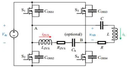
The circuit diagram and ideal operating waveforms of the PDM ZVS full-bridge converter described in [18] are shown in Fig. 1 and Fig. 2, respectively. The pulse density d of the switch-node voltage uAB is modulated to control the
equivalent conversion ratio when driving a resonant load. A ZVS branch that consists of a ZVS inductor LZVS and a dc
blocking capacitor Cb is connected between the switch nodes
A and B to provide a ZVS current iZVS that
charges/discharges the switch output capacitances COSS1-4
in dead-time transients to achieve soft switching. The equivalent series resistance (ESR) of the ZVS branch is denoted by RZVS .
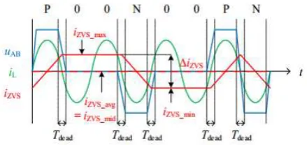
The waveforms shown in Fig.2 were derived from the existing PDM strategy [18], whose block diagram is shown in Fig. 3. The strategy was elaborately designed to generate a symmetric iZVS to ensure the ideal ZVS for minimizing
the switching loss. However, the converter with the existing PDM strategy suffers from the limitations of 1) large low-frequency subharmonics on uAB, 2) a narrowed modulation
[image:1.595.333.547.592.705.2]range, and 3) a large modulation delay. The large low-frequency subharmonics are created by the nested frequency modulator “FM” and lead to large ripples on the converter input and output power. The modulation range is narrowed by the lower limit on the pulse density d. The limit is to prevent “FM” from falling into a too long modulation period but it reduces the range of conversion ratio. The large modulation delay is introduced by the small accumulation coefficient ke that ensures the stability of the delta-sigma loop.
Fig -1: Circuit diagram of PDM ZVS full-bridge converter
This paper finds that even with an asymmetric iZVS, the
ideal ZVS can still be ensured if Cb is removed, waveforms
© 2019, IRJET | Impact Factor value: 7.211 | ISO 9001:2008 Certified Journal
| Page 6832
average (−0.5 A) and a near-zero midrange, and the absolutevalues of the minimum and maximum iZVS both equal the
[image:2.595.57.277.145.249.2]optimal current (1 A) for ideal ZVS.
Fig .2. Ideal operating waveforms with the existingPDM strategy
The mechanism is explained in Section II by the topology and principle and Section III by the negative feedback effect of the dead-time voltage. By using this effect, Section IV proposes a simplified PDM strategy that allows asymmetric iZVS and
overcomes the limitations of the existing PDM strategy. A WPT system are given in Section V and Section VI shows the simulation result, respectively. Section VI concludes the paper
2. TOPOLOGY AND PRINCIPLE
Fig. 1 shows the schematic of the main circuit of the proposed PDM ZVS full-bridge converter that operates in inversion mode. The converter is fed by a dc input voltage of magnitude vin and drives a series resonant tank, which has inductance L, capacitance C, and resistance R. The converter is comprised of a conventional full bridge with switches S1-4 and a ZVS branch that consists of a ZVS inductor LZVS and a dc
blocking capacitor Cb. The ZVS branch is connected between
the two switching nodes A and B of the two half bridges. Fig. 2 shows the ideal waveforms when the pulse density d of uAB equals 0.5. As compared with conventional full-bridge converters, some pulses of uAB are removed and the blanks are denoted by “0”. The ratio of the number of remaining positive (P) and negative (N) pulses to the total number of P, N and “0” is called pulse density d.
If the switching frequency fs of the pulses equals the resonant frequency fr, i.e.
The resonant current iL will be in phase with uAB, as shown
in Fig. 2. As per the “magnitude-density balance” principle [5], the root-mean-square (RMS) value of the fundamental component of uAB at fs is
Therefore, d is the control degree of freedom
of the converter. If Cb is large enough, such that
The absolute peak value of iZVS is
To fully discharge the switch output capacitance during dead time Td, |iZVS_pk| must be large enough and the
range of LZVS is given by
where COSSQ is the charge equivalent switch output
capacitance
2. NEGATIVE FEEDBACK EFFECT OF DEAD-TIME
VOLTAGE
2.1
Dead-time Transients and Switching Modes
As shown in Fig.2 and Fig. 4, a PDM ZVS full-bridge converter may have six types of dead-time transients when uAB changes between the positive (P), negative (N), and
zero (0) states. In Fig. 5, the six types of transients are denoted by 1) Nto-0, 2) 0-to-P, 3) N-to-P, 4) P-to-0, 5) 0-to-N, and 6) P-to-N, respectively, and classified into two groups, i.e. the rising transients and the falling transients. Within the transients, the load current iL is neglected because it crosses
zero when the load is tuned at resonance, and iZVS is
treated as constant because the dead-time period Tdead is
much shorter than the pulse width of uAB. The values of iZVS
in the three types of rising transients are assumed to be identical and equal the minimum value iZVS_min. Similarly,
the values of iZVS in the falling transients are assumed to
equal the maximum value iZVS_max.
The boundary current values are ioptimal, −ioptimal, and 0, where ioptimal is the optimal current for ideal ZVS, i.e. the minimum current that can fully charge/discharge the switch output capacitances in a dead time period:
COSSQ is the charge equivalent switch output
capacitance, which is a function of the converter dc side voltage Vdc
2.2 Dead-Time Voltage
The integrals of uAB during dead-time transients are
functions of iZVS_min and iZVS_max, and can be
expressed as the midrange ZVS current iZVS_mid and
the peak-to-peak ZVS current Δizvs as
(1)
(2)
(3)
(4)
(5)
(6)
© 2019, IRJET | Impact Factor value: 7.211 | ISO 9001:2008 Certified Journal
| Page 6833
ΔiZVS is determined by the relationship of
where Ts is the fundamental switching period, i.e. the switching period when d = 1. When the ZVS inductance is optimized as
2.2 The Negative Feedback Effect
Since the densities of the positive and negative pulses in uAB are equal, the average of uAB depends only on uAB_Tdead_avg:
3. PROPOSED PDM STRATEGY
3.1Operating Principle
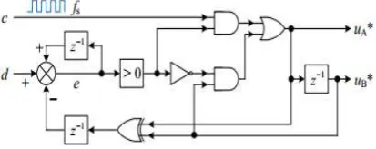
Utilizing the negative feedback effect of the dead-time voltage, a simplified PDM strategy that allows asymmetric ZVS currents is proposed for the ZVS full-bridge converters without dc blocking capacitors. The block diagram of the strategy is shown in Fig. 3.
[image:3.595.36.274.93.207.2]The input signals include a continuous pulse c and a specified pulse density d. The frequency of c equals the fundamental switching frequency fs = 1/Ts. The range of d is [0, 1]. The output signals are uA* and uB*, which are the references for the switch nodes A and B, respectively. The strategy uses an adder, a comparator, five logic gates, and three delay units. The delay units are triggered by the rising and falling edges of c. Therefore, the iteration frequency of the strategy is 2fs. In each iteration, the difference between d and uA* XOR uB* is accumulated and the result is denoted by e. If e > 0, uA* equals c, otherwise equals the previous uA*. uB* always equals the previous uA*.
Fig -3: Block diagram of the proposed PDM strategy
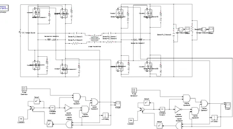
[image:3.595.307.562.322.654.2]4. THE WPT SYSTEM
Fig. 4 shows a WPT system that employs PDM ZVS fullbridge converters on both transmitting and receiving sides as inverter and rectifier, respectively.The inverter converts the input dc voltage vinto its switching node voltage u1and injects energy into the transmitting side resonator, which has inductance L1, capacitance C1, and equivalent series resistance(ESR) R1. The resonant current on the transmitting side is denoted by iL1. Symmetrically, the rectifier converts the output dc voltage voto its switching node voltage u2and absorbs energy from the receiving side resonator, which has inductance L2, capacitance C2, and ESR R2. The resonant current on the receiving side is denoted by iL2. In addition, the mutual inductance between L1and L2is M, the filter capacitance is Cf, and the load resistance is RL.
Table -1: CONVERTER PARAMETERS
SL.
NO
QUANTITY
SYMBOL VALUE
1. Converter dc side voltage 40V
2. Dead time period 50ns
3. Charge equivalent switch output capacitance 600pF
4. Optimal current for ideal ZVS 1A
5. Fundamental switching period 1µs
6. Fundamental switching frequency 1MHz
7. ZVS inductance 10µH
8. Peak-to-peak ZVS current 2A
9. ZVS branch resistance 0.1Ω
(8)
(9)
(10)
[image:3.595.79.286.656.738.2]© 2019, IRJET | Impact Factor value: 7.211 | ISO 9001:2008 Certified Journal
| Page 6834
Fig -4: Circuit diagram of the WPT systemThe transmitting side modulator modulates u1using an independent clock signal and a specified pulse density d1.
The RMS value of the fundamental component of u1is
[image:4.595.43.282.98.278.2]The receiving side modulator modulates u2using the pulses synchronized with iL2and a specified pulse density d2. The RMS value of the fundamental component of u2is
Table -2:
PARAMETERS OF THE WPT
SL.NO SYMBOL QUANTITY VALUE
1. Resonant inductances 75.3 μH
2. Resonant capacitances 400 pF
3. Resonant frequencies 0.917 MHz
4.
Fundamental switching
frequency 0.917 MHz
6. SIMULATION RESULTS
6.1 Steady-State Performances
[image:4.595.53.532.468.734.2]The steady-state performances of the converter were tested to confirm the ZVS operation and investigate the subharmonics of uAB. The measured power losses of the converter with different d were about 0.2 W, which were much lower than the calculated hard switching power losses, indicating that the ZVS was achieved by both the two PDM strategies. The measured waveforms when d = 0.5 compares the subharmonics of |uAB| with normalized units.
|uAB| is of interest because the positive and negative pulses
© 2019, IRJET | Impact Factor value: 7.211 | ISO 9001:2008 Certified Journal
| Page 6835
subharmonic at 0.25fs was eliminated by the proposed one.As the remaining subharmonics were concentrated closer to fs, the power flow can be controlled more smoothly and the electromagnetic interferences can be suppressed more easily. Similar results were also obtained with different d.
Fig.5. Proposed pdm strategy
6.2 Sinusoidal Responses
The sinusoidal responses of the converter were tested to investigate the range of the achievable d. The measured responses when the specified d = 0.5+0.5sin(4000πt), i.e. a biased 2 kHz sine wave with a maximum of 1 and a minimum of 0. The existing PDM strategy needed an appropriate lower limit on d to ensure the stability and continuous operation, while the proposed one could accurately follow the specified d, covering the full range of [0, 1].
6.3 Step Responses
The step responses of the converter were tested to investigate the modulation delay. The measured responses when the specified d steps between 0.2 (the lower limit of the existing PDM strategy) and 1. With the existing PDM strategy, the modulation delays were about 4 μs (4Ts) and 10 μs (10Ts) for the step up and down, respectively, depending on the accumulation coefficient ke. In contrast, uAB responded to the changes of d immediately when using the proposed PDM strategy. The fast response can simplify the system level dynamical analysis and control [20-22] as the modulation can be treated as ideal
Fig.6. Pulse density values of D1=0.89,D2=0.90
Fig.7. Pulse density values of D1=0.705,D2=0.65
© 2019, IRJET | Impact Factor value: 7.211 | ISO 9001:2008 Certified Journal
| Page 6836
Table -3:REPORTED WPT SYSTEMS WITH MEPT
INPUT
VOLTAGE D1 D2
OUTPUT DC VOLTAGE INPUT DC POWER OUTP UT DC POWE
R
EFFIC ENCY
40V 0.70 0.6 40V 39.1W 31.50
W 80%
40V 0.46 0.5 40V 19.6W 16.0W 82%
40V 0.89 0.9 40V 17.5W 15.3W 88%
3. CONCLUSIONS
In a ZVS full-bridge converter, the switch-node voltage in dead-time transients depends on the ZVS current. The average switch-node voltage in multiple dead-time transients can provide a strong negative feedback effect that pushes the midrange ZVS current toward zero regardless of its average value so that the ideal ZVS can be ensured even with an asymmetric ZVS current. This effect is utilized by the proposed PDM strategy to overcome the limitations of the existing PDM strategy for ZVS full-bridge converters. As compared with the existing one, the proposed PDM strategy exhibits lower low frequency subharmonics, wider modulation range, and faster response. With these advantages, PDM ZVS full-bridge converters can be one of the ideal choices for WPT systems.
REFERENCES
[1] C. T. Rim and C. Mi, Wireless Power Transfer for Electric Vehicles and Mobile Devices. John Wiley & Sons, 2017 [2] A. Daga, J. M. Miller, B. R. Long, R. Kacergis, P.
Schrafel, and J. Wolgemuth, "Electric fuel pumps for wireless power transfer: enabling rapid growth in the electric vehicle market," IEEE Power Electron. Mag., vol. 4, no. 2, pp. 24-35, 2017.
[3] C. C. Mi, G. Buja, S. Y. Choi, and C. T. Rim, "Modern advances in wireless power transfer systems for roadway powered electric vehicles," IEEE Trans. Ind. Electron., vol. 63, no. 10, pp. 6533-6545, 2016.
[4] S. Y. Choi, B. W. Gu, S. Y. Jeong, and C. T. Rim, "Advances in wireless power transfer systems for roadway-powered electric vehicles," IEEE J.Emerg. Sel. Topics Power Electron., vol. 3, no. 1, pp. 18-36, 2015.
[5] G. A. Covic and J. T. Boys, "Modern trends in inductive power transfer for transportation applications," IEEE J. Emerg. Sel. Topics Power Electron., vol. 1, no. 1, pp. 28-41, 2013.
[6] S. Y. R. Hui, W. X. Zhong, and C. K. Lee, "A critical review of recent progress in mid-range wireless power transfer," IEEE Trans. Power Electron., vol. 29, no. 9, pp. 4500-4511, 2014.
[7] G. A. Covic and J. T. Boys, "Inductive power transfer," Proc. IEEE, vol.101, no. 6, pp. 1276-1289, 2013.
[8] J. T. Boys and G. A. Covic, "The inductive power transfer story at the University of Auckland," IEEE Circuits Syst. Mag., vol. 15, no. 2, pp. 6-27, 2015. [9] H. Li, J. Li, K. Wang, W. Chen, and X. Yang, "A maximum
efficiency point tracking control scheme for wireless power transfer systems using magnetic resonant coupling," IEEE Trans. Power Electron., vol. 30, no. 7, pp. 3998-4008, 2015.
[10] H. Li, J. Fang, S. Chen, K. Wang, and Y. Tang, "Pulse density modulation for maximum efficiency point tracking of wireless power transfer systems," IEEE Trans. Power Electron., vol. 33, no. 6, pp. 5492-5501,2018.
[11] M. Fu, H. Yin, M. Liu, and C. Ma, "Loading and power control for a high efficiency class E PA-driven megahertz WPT system," IEEE Trans. Ind. Electron., vol. 63, no. 11, pp. 6867-6876, 2016.
[12] X. Dai, X. Li, Y. Li, and A. P. Hu, "Maximum efficiency tracking for wireless power transfer systems with dynamic coupling coefficient estimation," IEEE Trans. Power Electron., vol. 33, no. 6, pp. 5005-5015,2018. [13] W. Zhong and S. Y. R. Hui, "Maximum energy efficiency
operation of series-series resonant wireless power transfer systems using on-off keying modulation," IEEE Trans. Power Electron., vol. 33, no. 4, pp. 3595-3603,2018.
[14] Z. Huang, S.-C. Wong, and C. K. Tse, "Control design for optimizing efficiency in inductive power transfer systems," IEEE Trans. Power Electron., vol. 33, no. 5, pp. 4523-4534, 2018.
[15] M. F. Fu, H. Yin, X. E. Zhu, and C. B. Ma, "Analysis and tracking of optimal load in wireless power transfer systems," IEEE Trans. Power Electron., vol. 30, no. 7, pp. 3952-3963, 2015.
[16] H. Li, K. Wang, J. Fang, and Y. Tang, "Pulse density modulated ZVS fullbridge converters for wireless power transfer systems," IEEE Trans.Power Electron., vol. 34, no. 1, pp. 369-377, 2019.
[17] M. A. de Rooij, "The ZVS voltage-mode class-D amplifier, an eGaN FETenabled topology for highly resonant wireless energy transfer," in Proc.IEEE Appl. Power Electron. Conf. Expo., 2015, pp. 1608-1613.
[18] Z. U. Zahid, Z. Dalala, and J. S. J. Lai, "Small-signal modeling of seriesseries compensated induction power transfer system," in Proc. IEEE Appl.Power Electron. Conf. Expo., 2014, pp. 2847-2853.