Simulation of III-V Material Based Steep Slope Tunnel FET for RF
Harvester Application
Saravana Selvan
1, 2,*, Goh Kooh Yik
2,
Gobbi Ramasamy
1, Mukter Zaman
11Faculty of Engineering, Multimedia University, Cyberjaya, Malaysia 2Faculty of Engineering & Computer Technology, AIMST University, Bedong, Malaysia
Received 20 July 2018; received in revised form 29 August 2018; accepted 16 October 2018
Abstract
Due to the limitation of Sub-threshold Swing (SS) of 60 mV/dec in CMOS, alternately Tunnel FETs (TFETs) are more attractive in recent years since it has high energy efficiency and better switching performance even at a reduced voltage level. Because it has the benefits of Band to Band Tunneling (BTBT) behavior of operating mechanism and achieved a steep slope characteristic of less than 60 mV/dec. Despite these merits due to the band to band tunneling, the conventional Silicon based TFET is suffered from very low and limited ON-state current due to indirect and large energy gap feature. In the indirect band gap, the conservation of momentum occurs only when the absorption and emission of a photon are required which makes the absorption coefficient lower and limits the flow of electron. To address this problem, in this paper, a Hetero-Junction Tunnel FET (HTFET) devices employing with different lower bandgap materials (InAs/GaSb and InGaAs/InP) are designed by using Silvaco TCAD device simulator. The overall DC and analog/RF performance of HTFET devices are being extracted and investigated suitable for RF energy harvesting applications. The InAs/GaSb HTFET has shown a superior in characteristics by achieving a higher ON-state current of 2.3 mA/µm at Vgs = 1V, OFF current leakage of 4.18 x 10⁻¹¹ A/µm, SS of 22.18 mV/dec and cut-off frequency range from MHz to GHz in operation. Under very low ambient RF level or sub-milliwatt (< 0 dBm) level conditions, the conventional CMOS based rectifier in RF harvester shows very poor performance and probably fails to convert RF signal into DC output voltage. This is due to the SS limitation of 60 mV/dec. Hence, HTFET based RF harvester is proposed and implemented in the circuit level by using the Keysight ADS software. The result indicates that a two-stage Dickson voltage multiplier design using InAs/GaSb HTFET can able to produce a DC output of 1.9 V, 1.6 µA @ 0 to -10 dBm, maximum efficiency of 59 % @ -14 dBm, operating frequency of 850 MHz at 10 kΩ loads with a sensitivity of 0 to -25 dBm.
Keywords: tunnel FET, band to band tunneling (BTBT), sub-threshold Swing (SS), RF harvester
1.
Introduction
In recent decades, the continuous downscaling of CMOS creates a fundamental performance limitation such as short channel effects, high power dissipation due to leakage currents, low Ion/Ioff current ratio and sub-threshold Slope (SS of ≥ 60 mV/dec) at room temperature [1-2]. This is due to the phenomenon of drift-diffusion injection carrier mechanism in current MOSFETs. Hence the research is being carried out to find a new alternate device. Recently Tunnel FET has attracted huge attention and a most promising device for ultra-low power analog and digital circuits because it offers very low leakage current, low power dissipation, the steep sub-threshold slope of (less than 60 mV/dec) and fits best into the low standby power region [3-5]. TFETs are highly immune to short channel effects due to the band to band tunneling behavior of
*Corresponding author. E-mail address: [email protected]
injection carrier mechanism on the source side as well as the scaling of gate length is possible along with the tunneling barrier width of less than 5nm. Moreover, TFET is independent of thermal factor kT/q not likely in MOSFETs. Silicon-based TFET is highly preferred since it can be easily fabricated and manipulate because of the existing CMOS technology supports it. However, the performance of Si-TFET is very poor in terms of ON-state current compared to MOSFETs due to indirect and large energy gap [6-7] and it fails to achieve the required current for the advanced technology nodes [8].
To overcome the above problem, recently a number of techniques were proposed by the researchers in their work by using high-k gate dielectric [9], gate stacking [10], strain engineering [11], and by using lower band gap material [12]. In order to accomplish a large on-drive current in TFET, small bandgap materials are desirable. Germanium (Ge) is also similar to Si, which is more CMOS compatible. It has been attracted by most of the researchers because of the very small gap of 0.67 eV compared to Si. However, it can increase the current mobility but it suffers from large leakage current [13]. Some of the research works have included the hetero-junction of both Si and Ge for attaining higher ON state current [14]. Next, to the Si and Ge, small band gap with low energy mass and higher tunneling probability properties of III-V compound materials are preferred [15]. By combining the metallic group III from the periodic table and the non-metallic group V from the periodic table, III-V compound material is formed. The application of III-V materials such as InAs, GaSb, InGaAs, AlGaSb, GaAsSb etc., are quite promising to be used for designing the TFET in recent days [16]. There are some simulation studies were performed by the researchers to find the physical insights of TFET and optimize the device design for enhancing the performances [17-18]. However, still, there are challenging remains in the III-V semiconductor-based TFET to achieve a very good steep sub-threshold slope and analog characteristics suitable for ultra-low power applications. Hence in this work, a TCAD simulation study of hetero-junction and different low band gap materials of InAs/GaSb and InGaAs/InP based TFETs are investigated. Since the effective tunneling mass of III-V materials is small compared to tunneling mass of Si. To enhance the electro-static control of drain currents through the gate electrode, a double gate structure is employed in both the TFETs. The III-V material based TFETs considered in this work are simulated in Silvaco TCAD and their performances are analyzed in terms of output dc characteristics and analog/RF parameters. Finally, an ultra-low power RF energy harvester application is chosen for implementing our HTFET.
2.
Device Structure and Simulation Setup
TFET is a three terminal device similar in structure to MOSFET. The n-type TFET consists of P+ doped acting as a source, an intrinsic channel of I, and N+ doped region acting as a drain terminal. The height of the channel barrier height is controlled by the electrostatic control of the gate terminal voltage like same in MOS transistor. The operating mechanism of TFET is unique and different from MOSFET. The basic operating mechanism of TFET is based on Band-To-Band Tunneling (BTBT). BTBT involves tunneling of carriers from the valence band into the conduction band through the forbidden band gap or vice versa. Band diagrams of an n-type TFET are shown in Fig. 1(a) in the OFF-state and in the ON-state. When the gate voltage is close to zero, the TFET is in the OFF-ON-state. The conduction band in the channel lies above the valence band in the source. As a result, BTBT is inhibited and the TFET is in the OFF-state with extremely low drain current. When the gate voltage is increased, the gate voltage modulates the carrier density below the gate and the conduction band in the channel is pushed down. When a sufficiently high voltage is applied to the gate, there is band bending at the source such that the valence band in the source and the conduction band in the channel get aligned, as shown in Fig. 1(a). As a result, the electrons in the valence band of source terminal can tunnel into the conduction band of the channel. The electrons that tunnel into the channel are swept to the drain terminal by the positive bias of the drain. The band diagrams of a p-type TFET in OFF-state and ON-state are shown in Fig. 1(b).
blocked and the TFET is in the OFF-state. When a sufficiently large negative voltage is applied to the gate, the valence band in the channel is pushed above the conduction band of the source as shown in Fig. 1(b). As a result, holes are injected into the channel, which is subsequently swept to the drain terminal by the negative bias of the drain. The high energy carriers distributed in the Fermi-Dirac tail are rejected by the band gap in the source and hence it cannot contribute to the movement process [19]. It is fundamentally the lower temperature of carriers involved in the transportation process through tunneling window which results in a steep slope SS of less than 60 mV/dec. The tunneling probability of electrons across the potential barrier in the source-channel TFET junction is analytically solved by WKB (Wentzel Kramers Brillouin) approximation [20] as
(a) n-type TFET in OFF state and ON state (b) p-type TFET in OFF state and ON state
Fig. 1 BTBT Operation of n-type TFET and p-type TFET
2
exp 4 2
* 3
3
g Si
D ox Si
ox g
m E
I T b b t t
eh E
(1)
where m* and Eg is the carrier effective mass and energy band gap of material, ∆φ stands for energy range where tunneling is taking place, e is the charge of electron and h is Planck’s constant. εox and εsi is the dielectric of oxide and body substrate respectively. tox and tsi is the thickness of oxide and body substrate respectively.
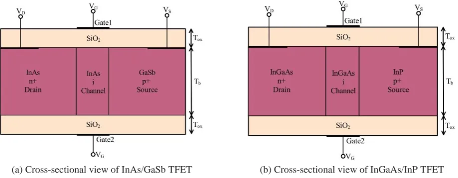
(a) Cross-sectional view of InAs/GaSb TFET (b) Cross-sectional view of InGaAs/InP TFET
Fig. 2 The cross-sectional view of III-V material based HTFET devices
values are lower than the conventional Si. The reduced effective mass value of holes and electrons has the advantage of an increase in tunneling the barrier. The high mobility and direct band gap feature of III-V materials can also improve the tunneling current.
Table 1 Material Parameters used in the simulation
Parameters InAs GaSb InGaAs InP
Effective mass of electron tunneling (me) 0.023 0.042 0.043 0.08 Effective mass of hole tunneling (mh) 0.4 0.4 0.052 0.012
Mobility of electron (cm2/V.s) 33000 5000 12000 5400 Mobility of Hole (cm2/V.s) 400 850 300 200
Energy Band Gap Eg (eV) 0.36 0.72 0.75 1.35
Permittivity 15.15 15.7 13.9 12.5
A common double gate electrode structure is chosen in this work because it gives better electrostatic control on the channel of the device. The combined effect features of material engineering will reduce the energy barrier at source-channel junction leads to improve the BTBT rate and SS. III-V materials of 10nm body thickness and gate oxide material of SiO2 with a dielectric value of ε=3.9 is chosen for this study. The device design parameters used in the TCAD simulations are shown in Table 2.
Table 2 Device design parameters used in the simulation
Parameters Value
SiO2 layer thickness (Tox) 1.5 nm
Body Thickness (Tb) 10 nm
Source length (Ls) 50 nm
Gate length (Lg) 20 nm
Drain length (Ld) 50 nm
Source, Channel & drain doping 1x10
22 atoms/cm-3, 1x10¹⁶ atoms/cm-3 & 1x10¹⁹ atoms/cm-3 Gate 1 & Gate 2 metal work function 4.5 eV (Chromium)
To do an extensive simulation of III-V TFET devices, Silvaco 2D Atlas device simulator is used in this work [21]. The non-local band to band tunneling model is employed in this simulation for modeling the tunneling process accurately as well as considering the spatial variation of energy band. To introduce the trap-to-band phonon-assisted tunneling in our device, trap assisted model is considered. The tunneling probability across the junction is calculated by using the Wentzel-Kramers-Brillouin (WKB) method. Shockley-Read-Hall (SRH) generation and recombination model is adopted to include the effect of carrier recombination and account the leakage currents. To account the transfer of electrons and holes in the simulation, the drift-diffusion transport model is considered. To incorporate the temperature dependent carrier mobility, Lombardi Constant Voltage Temperature (CVT) mobility is used [22]. Since the body thickness of our simulated III-V TFET devices is more than 5nm, here the quantum transport model and Band Gap Narrowing (BGN) is not considered in our work [23].
3.
TCAD Simulation Results and Discussion
3.1. DC performance analysis
probability of electrons moving from VB of the source to CB of the channel is taken place. However, it is observed that InAs/GaSb HTFET has closer alignment of energy gap on source-channel junction when compared to InGaAs/InP TFET. Since the energy band gap values of InAs and GaAs values are very less compared to InGaAs and InP values which can be referred to in Table 1.
(a) Energy band diagram of InAs/GaSb TFET (b) Energy band diagram of InGaAs/InP TFET
Fig. 3 Energy band diagram of III-V material based HTFET devices
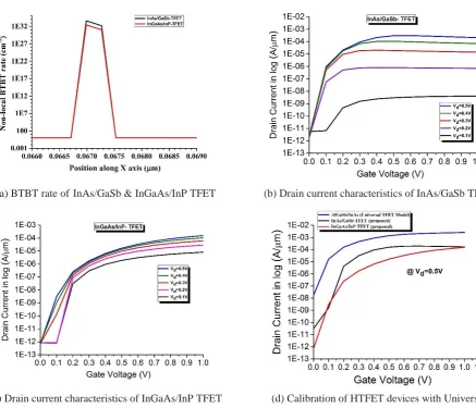
(a) BTBT rate of InAs/GaSb & InGaAs/InP TFET (b) Drain current characteristics of InAs/GaSb TFET
(c) Drain current characteristics of InGaAs/InP TFET (d) Calibration of HTFET devices with Universal
Fig. 4 BTBT rate and Drain current characteristics of III-V TFET devices
shown in Fig. 4(a). The high BTBT rate involves in the source channel interface leads to the flow of high ON state drain current. The drain current transfer characteristics of both the HTFET at different Vds values are shown in Fig. 4(b) and (c). There it can be seen that an ON-drive current of 1.59 x 10⁻⁴ A/µm and 1.65 x 10⁻⁵ A/µm achieved by both the devices InAs/GaSb and InGaAs/InP TFET at Vgs =0.5V & Vds= 0.5V respectively. Both the HTFET devices are comparatively giving very good drain current characteristics and it is calibrated with Universal TFET model as observed in Fig. 4(d). It is preferred that our simulated III-V devices curves are more or less try to achieve the same as Universal TFET characteristics. The Universal TFET model is available in nano-hub website [24] in which double gate AlGaSb/InAs is considered in this work as a calibrated model. The InAs/GaSb TFET achieved a maximum current value is 2.3 mA/µm at Vgs = Vds= 1V which is comparatively greater than InGaAs/InP TFET. The OFF current values can be extracted from Id-Vgs characteristics of a particular device and it is very important to be considered at ultra-low power applications. The obtained OFF-state current value of InGaAs/InP TFET is very low of 8.66 x 10⁻¹³ A/µm when compared with InAs/GaSb TFET of 4.18 x 10⁻¹¹ A/µm. The InGaAs/InP combination forms a staggered band alignment which creates a high depletion region or big tunneling barrier at the source-channel interface and makes the OFF-state current becomes lower. In the case of InAs/GaSb HTFET, although it has shown an improvement in high ON state current it shows a high OFF state current comparative than InGaAs/InP HTFET due to the formation of a broken gap. A very low value of device OFF current indicates that standby power consumption to be very low when it is used in analog and digital circuits.
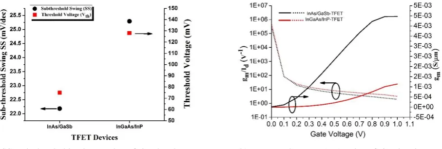
The point sub-threshold slope is calculated by taking the maximum slope of the log Id versus Vgs curve. The calculated values are 22.18 and 21.11 mV/dec respectively. The average SS of the simulated device is calculated by using the Eq. (2).
t off
vt off
V V SS
LogI LogI
(2)
The calculated SS values of InAs/GaSb HTFET and InGaAs/InP HTFET are 22.18 and 25.29 mV/dec respectively. It is noted that very low SS achieved by III-V TFET device indicates a very steeper slope characteristic. Hence it is expected that a higher Ion/Ioff ratio can be obtained even at a very low supply voltage of less than 0.5 V. The HTFET devices achieve a higher Ion/Ioff ratio of 109. Hence, it can be a promising device for a reduced dynamic power dissipation of digital circuits. Due to the very steep SS and very low OFF-state leakage current of HTFET, it will lead to having a low threshold or turn-on voltage. The calculated threshold voltage value of simulated HTFET devices is 75 mV and 128 mV respectively. The calculated SS and threshold voltage values for simulated III-V TFET devices are shown in Fig. 5(a). The SS achievement of less than 60 mV/dec achieved by the simulated III-V TFET devices indicates that its switching speed is very high which is very essential in the case of ultra-low power and energy efficient applications. In addition to that, OFF state leakage and the threshold voltage parameter trade-offs can be relaxed because of the tunneling operating mechanism. The achievement of low threshold voltage indicates that the device sensitivity can be increased. From the DC analysis response of simulated III-V TFET devices, it is observed to be suitable for ultra-low power applications.
3.2. Analog/Radio Frequency (RF) performance analysis
D m
GS I g
V
(3)
The value of gm with the variation of Vgs, atVds = 1V for the HTFET devices are shown in Fig. 5(b). As per the Eq. (3), the value of gm is directly depended on the exponential increase in the value of the drain current (Id). The simulated InAs/GaSb HTFET device has a good exponential increase in Id with the variation of Vgs characteristics, and then it achieves a higher gm value of 1.65 x10
-3 (S/μm). The higher value of g
m providedby the HTFET devices which mean it can be a suitable choice for analog amplification circuits. In the same Fig. 5(b) (refer dotted line), the variation of Transconductance to the current ratio (gm/Id) with the increase in Vgs is also shown. It is referred to as a governing factor for the net transconductance generation efficiency of a device. It represents the efficiency of the device to convert the bias current into transconductance. This parameter is strongly related to analog performance (i.e) higher the gm/Id value ensures the better amplification per unit drain current. In the low sub-threshold region of Vgs less than 0. 1V, both the HTEFT devices provide a very high gm/Id of around 5 x 10⁵ (V-1). As the Vgs increases further, the gm/Id value of both the HTEFT gets degrades very faster. Hence it is very difficult to provide the linear output to the circuit’s level. However, it can be most suitable for the design of ultra-low power analog circuit applications. It is noted that simulated III-V HTFET devices are having non-linearity problem and there is a lack of noise performance analysis, which may be considered as future work. Then only the prediction of analog performance would be complete.
(a) SS and Threshold voltage value of simulated TFET (b) Transconductance (gm) value of simulated TFET
Fig. 5 SS, Threshold voltage and Transconductance (gm) value of simulated III-V TFETs
The variation of output conductance (gd) with Vds for III-V TFET devices at Vgs = 1V are shown in Fig. 6(a). It is observed that at a lower value of Vds, the drain control decreases and the drain current rises non-linearly. As a result, it provides a small increase in the output conductance (gd) until a certain Vds voltage of 0.5V. After that, it enters into the saturation region. This minimum value of gd isobtained due to Drain Induced Barrier Lowering (DIBL) and channel length modulation, so the current is constant in the saturation region. In the same time, at a reduced gate voltage of Vgs, there is a sufficient drain control at a lower value of Vds. Hence it can be predicted that the III-V HTFET simulated devices have more advantages in producing high gains at low power supply because the gd decreases at a lower value of Vgs and Vds. However, at under low Vgs, theoutput resistance (r0) of HTFET shows larger since there is no PN junction formed on the drain side. It can be clearly observed from (r0) curve in Fig. 6(a) which is exactly the inverse of gd. It is calculated that InAs/GaSb TFET and InGaAs/InP TFET obtains a minimum DIBL value of 135.6 mV/V and 44.4 mV/V respectively. It can be employed to achieve a higher value of intrinsic gain Av by
.
m
v m o
d
g
A
g r
g
(a) Variation of gd and r0 as a function of
drain voltage at Vgs = 1V (b) Intrinsic gain of simulated device at Vds=1V
Fig. 6 Output conductance (gd), Output resistance (r0), and Intrinsic gain of simulated III-V TFET devices
The Fig. 6(b) shows the Intrinsic gain of the simulated device with respect to the gate to source voltage at Vds=1V in which InGaAs/InP TFET has achieved a higher gain compare to InAs/GaSb TFET. Since the output conductance (gd) and output resistance (r0) values are very low values over the variation of the gate voltage as referred to in Fig. 6(a). The proposed InGaAs/InP TFET can provide a high intrinsic gain Av of 24.5 at a gate voltage of 0.1 V.
(a) Gate to drain capacitance (Cgd) values (b) Gate to source capacitance (Cgs) values
Fig. 7 Gate to drain capacitance (Cgd) and Gate to source capacitance (Cgs) values of III-V TFETs at Vds=1V
2m T
gd gs g f
C C
(5)
2 m
gd
g GBP
C
(6)
FT is the transient frequency where the current gain of the device becomes unity and GBP is the measure of the device performance in high-frequency ranges calculated at DC gain of 10. InAs/GaSb TFET has very good fT response and achieves a higher frequency value (in GHz range) at lower Vgs as shown in Fig.8(a).This is due to the combined effect of the higher value of gm at smaller Vgs and the reduced value of Cgs + Cgd. Similarly, it is noticed that GBP value for InAs/GaSb TFET is a significantly higher range in frequency compared to the InGaAs/InP device due to the effect of lower Cgd as shown in Fig. 8(b). Thus, the simulated hetero-junction InAs/GaSb and InGaAs/InP TFET devices will be suitable for high radio frequency circuit and ultra-low power applications. The summary of simulated III-V material based TFET results are tabulated in Table 3. It is observed that both the simulated TFETs are achieved a very good DC and analog characteristics at very low gate voltages.
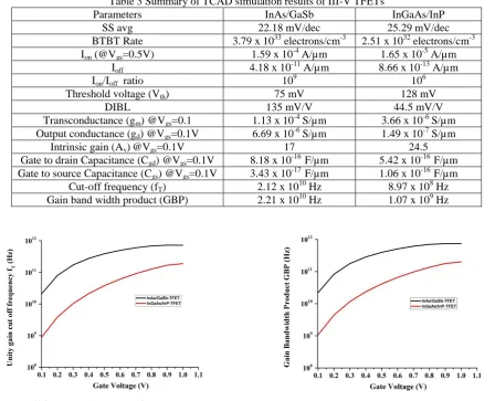
Table 3 Summary of TCAD simulation results of III-V TFETs
Parameters InAs/GaSb InGaAs/InP
SS avg 22.18 mV/dec 25.29 mV/dec
BTBT Rate 3.79 x 1033 electrons/cm-3 2.51 x 1032 electrons/cm-3 Ion (@Vgs=0.5V) 1.59 x 10⁻⁴ A/µm 1.65 x 10⁻⁵ A/µm
Ioff 4.18 x 10⁻¹¹ A/µm 8.66 x 10⁻¹³ A/µm
Ion/Ioff ratio 109 106
Threshold voltage (Vth) 75 mV 128 mV
DIBL 135 mV/V 44.5 mV/V
Transconductance (gm) @Vgs=0.1 1.13 x 10⁻⁴ S/µm 3.66 x 10⁻⁶ S/µm Output conductance (gd) @Vgs=0.1V 6.69 x 10⁻⁶ S/µm 1.49 x 10⁻⁷ S/µm
Intrinsic gain (Av)@Vgs=0.1V 17 24.5
Gate to drain Capacitance (Cgd) @Vgs=0.1V 8.18 x 10⁻¹⁶ F/µm 5.42 x 10⁻¹⁶ F/µm Gate to source Capacitance (Cgs) @Vgs=0.1V 3.43 x 10⁻¹⁷ F/µm 1.06 x 10⁻¹⁶ F/µm Cut-off frequency (fT) 2.12 x 10¹⁰ Hz 8.97 x 10⁸ Hz Gain band width product (GBP) 2.21 x 10¹⁰ Hz 1.07 x 10⁹ Hz
(a)Cut-off frequency fT values of simulated TFETs (b) Gain band width product (GBP) of simulated TFETs
Fig. 8 Cut-off frequency (fT) and gain band width product (GBP) variation with gate to source voltage at Vds = 1V
4.
TFET Modeling for RF rectifier
It has been referred from Table 3 that compared to InGaAs/InP TFET, the simulation results of InAs/GaSb TFET shows
that excellent linear current onset at the very low gate and drain voltages of 0.1 to 0.5V. It also noted that Radio Frequency
above TFET could be a suitable device for ultra-low power RF applications. Nowadays, RF energy harvesting circuits using
a rectifying antenna (rectenna) are getting more attention and it may be a viable solution for powering ultra-low power
sensors. Currently, the RF rectifier in the rectenna circuit is facing a major challenge that under very low ambient RF level
condition, it shows very poor performance and probably fails to convert RF signal into a required dc output voltage. This is
due to the subthreshold voltage limits or weak sensitivity of the rectifying device used in the rectifier [26]. Hence, our
simulated III-V TFET has the potential for supporting this RF rectifier circuit due to very steep slope characteristics and
superior performance at very low voltages [27]. To illustrate this potential, a lookup table based Verilog-A TFET model has
been employed for circuit simulations. The schematic of Verilog-A transistor model is shown in Fig. 9. The lookup table is
generated by extracting the model parameters based on TCAD simulations running at fine step drain-source voltage bias Vds
and gate-source voltage bias Vgs range from 0 to 50 mV. This lookup table model consists of two-dimensional tables having
the transfer characteristics Ids (Vds, Vgs), gate-source capacitance Cgs (Vds, Vgs), and gate-drain capacitances Cgd (Vds,
Vgs) values. The device transient characteristics are obtained through charge models. The drain and source terminal charge
(Qgs, Qgd) can be calculated by using Cgs and Cgd from lookup tables.
Fig. 9 Verilog-A TFET model Schematic
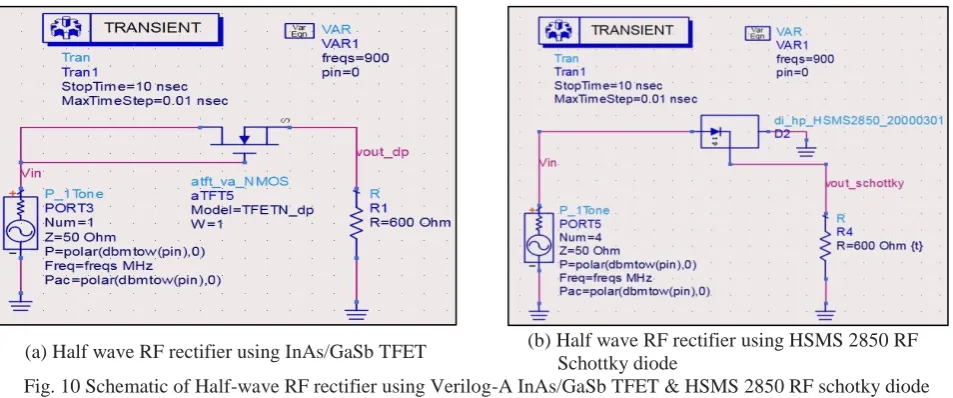
A simple half wave RF rectifier is designed by using Verilog A simulated III-V TFETs and Avago HSMS 2850
Schottky diode. The circuit consists of an RF power source input of 0 dBm at a frequency of 900 MHz is shown in Fig. 10.
The RF rectifier circuit is simulated by using Advanced Design System (ADS) software which is a commercial tool for RF
designers.
(a)Half wave RF rectifier using InAs/GaSb TFET (b) Half wave RF rectifier using HSMS 2850 RF
Schottky diode
Fig. 10 Schematic of Half-wave RF rectifier using Verilog-A InAs/GaSb TFET & HSMS 2850 RF schotky diode
(a) RF Input wave form at 900 MHz & 0 dBm (b) Rectified output voltage of HTFETs & HSMS 2850 Fig. 11 Simulated Input and Output waveforms of Half-wave RF rectifier using Verilog-A HTFETs & HSMS 2850
4.1. Implementation of simulated HTFETs in RF Harvester Circuit
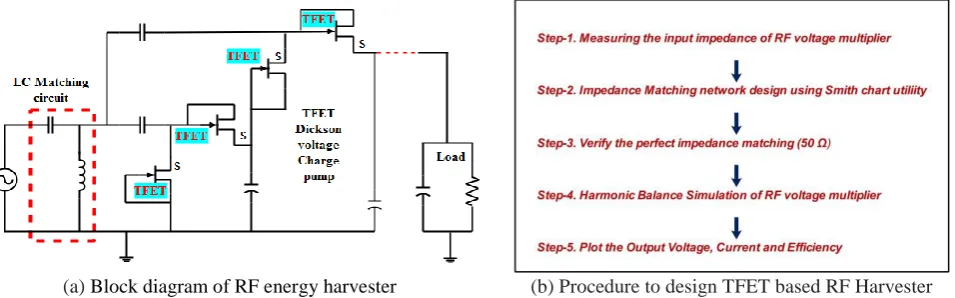
The general block diagram of RF energy harvester is shown in Fig. 12(a). It consists of receiving antenna as a source, impedance matching, and charge pump/voltage multiplier circuit. It is very challengeable to design when the harvester deals with very low RF power levels of less than 0 dBm available in the environment.
(a) Block diagram of RF energy harvester (b) Procedure to design TFET based RF Harvester Fig. 12 General block diagram and the steps followed to design TFET based RF Harvester
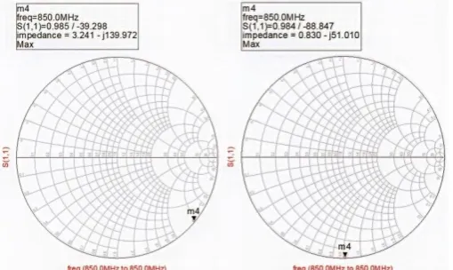
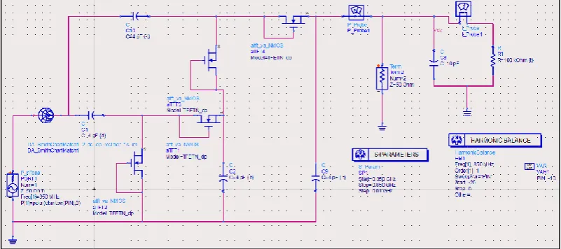
To design the RF harvester circuit, the design procedures to be followed exactly for efficient conversion of RF to DC output voltage. The steps involved in the Tunnel FET based RF harvester design using ADS software is shown in Fig. 12(b). Before going to the design steps, it was verified in the previous section that InAs/GaSb and InGaAs/InP TFETs can be modeled and operated as a diode in high-frequency input. In this work, the harvester operating frequency is set at 850 MHz for all the simulations because in most of the GSM mobile towers in Malaysia are sending the RF signal at this range only. The voltage multiplier is also known as the “charge pump” which is widely used in most of the Energy harvesting ICs. In this work, voltage multiplier made of Dickson topology connection is used for an improved DC output voltage. A two-stage TFET based Dickson voltage multiplier is proposed for minimizing the circuit size. The first stage of Dickson voltage multiplier is functioning as a rectifier only. To measure the input impedance of two-stage voltage multiplier, a port terminal impedance of 50 Ω is connected in both input and output of it. The S parameter simulator tool available in ADS software is used to find the input impedance value of it. By running an S parameter simulation at 850 MHz frequency, the input impedance value of two-stage voltage multiplier can be measured from the reflection coefficient S11 parameter which is shown in Fig. 13(a). The obtained values are 3.2-j140Ω and 0.83-j51Ω for InAs/GaSb and InGaAs/InP TFET based voltage multiplier circuits respectively. While measuring the input impedance value, we have considered the width of T1 = 40 um and T2 = 80 um.
The obtained input impedance value of the voltage multiplier circuit from the first step is added into the smith chart tool as load impedance Zload. The standard antenna impedance of 50 Ω is entered as source impedance Zsource on the smith chart. The schematic of the smith chart tool used in our design is shown in Fig. 13(c). The impedance matching values obtained by using smith chart for InAs/GaSb TFET based voltage multiplier are L= 28.53nH and C= 14.14pF. Similarly, we have obtained the impedance matching values for InGaAs/InP TFET based voltage multiplier circuits are L= 79.26nH and C= 3.60pF. It is necessary to verify that the whole RF harvester circuit impedance value should be around 50 Ω in the third step. This ensures that maximum power has been transferred from source to load. To verify it, again we need to measure the input impedance of the voltage multiplier with the addition of calculated LC matching elements between the source and load. It has been observed from Fig. 13(b) that the measured input impedance value with the inclusion of LC matching networks are 51.057-j0.855Ω and 49.99-j1.11Ω for InAs/GaSb and InGaAs/InP TFET based harvester circuits respectively.
(a) Measured input impedance value of InAs/GaSband InGaAs/InP TFET based harvester circuit
(b) Measured input impedance value of InAs/GaSb and InGaAs/InP TFET based harvester circuit with LC matching
(a) Measured input impedance value of InAs/GaSband InGaAs/InP TFET based harvester circuit
(b) Output results of current, voltage and efficiency of InAs/GaSb TFET based harvester circuit
(c) Output results of current, voltage and efficiency of InGaAs/InP TFET based harvester circuit
Fig. 14 Schematic design and DC output results of TFET based RF Harvester
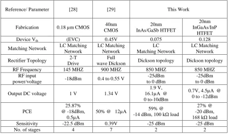
it can able to produce an output voltage of 1.9 V, a current of 16.1 µA @ 0 to -10 dBm which is shown in the Fig. 14(b). It can generate the maximum efficiency of 59 % @ -14 dBm at 100 kΩ loads with a sensitivity of -25 dBm. The comparative RF harvester simulation results are summarized in Table 4. Similarly, the InGaAs/InP TFET based RF harvester design generates the maximum efficiency of 27% @ -20dBm, 168 kΩ load with output voltage and current of 0.7 V and 4.5 µA @ 0 to -12dBm. The performance of InGaAs/InP TFET in RF harvester circuit is weak compared to InAs/GaSb TFET due to the formation of staggered band alignment design.
Table 4 Comparative summary of RF harvester simulation results using III-V TFETs
Then, in step II, the effect of the type of the carried cargo on the probability of theft was simulated. For this purpose,
10,000 transport cases, identical for each of the 12 types of cargo, were created. Based on the received data, it was possible
to compare the impact of the cargo type on the probability of theft.
In step III, the costs of loss were calculated based on the appropriate algorithms. For variant I - a carriage without cargo
monitoring systems and for variant II - a carriage with cargo monitoring systems, the cost of loss was calculated from Eq. (1).
5.
Conclusions
In this paper, two different III-V material InAs/GaSb & InGaAs/InP based hetero-junction TFET has been designed and simulated by using Silvaco 2D Atlas simulator. The designed TFET devices have been investigated in terms of DC and analog/RF performance Figure of Merits (FOMs). It has been observed that InAs/GaSb HTFET has shown better performance in terms of SS, drain current, gate to drain capacitance and frequency compared to InGaAs/InP HTFET, due to the formation of broken gap alignment. To implement the above HTFETs in circuit-level simulation, a look-up table based Verilog A TFET model has been created. A two-stage Dickson voltage multiplier based RF harvester made of Verilog A HTFETs has designed and studied. The Harmonic Balance simulation of InAs/GaSb TFET based RF harvester operates at 850 MHz provides the DC output voltage of 1.9 V, output current of 16.1 ”µA @ 0 to -10 dBm. It can generate the maximum efficiency of 59 % @ -14 dBm at 100 kΩ loads with a sensitivity of -25 dBm. Hence based upon this simulation study, InAs/GaSb III-V material based TFET could be a future device for ultra-low power RF harvester circuits.
Conflicts of Interest
The authors declare no conflict of interest.
Reference/ Parameter [28] [29] This Work
Fabrication 0.18 µm CMOS 40nm CMOS 20nm InAs/GaSb HTFET 20nm InGaAs/InP HTFET
Device Vth (EVC) 0.45V 0.075 0.128
Matching Network LC Matching Network LC Matching Network LC Matching Network LC Matching Network Rectifier Topology 2-T
Drive
Full
wave Dickson Dickson topology Dickson topology
RF Frequency 145 MHZ 900 MHZ 850 MHZ 850 MHZ
RF input
power/voltage -18dBm 0.4 to 0.55 V
-25dBm to 0 dBm
-25dBm to 0 dBm
Output DC voltage 1 V 1.34 V
1.9 V, 16.1µA @ 0 to-10dBm
0.7V, 4.5µA @ 0 to -12dBm
PCE
25.87% @ -18dBm,
0.5µA
50% @ 12µA 59% @
-14 dBm, 100 kΩ load
27% @ -20 dBm, 168 kΩ load
Sensitivity -22.5 dBm 0.39V -25 dBm -25 dBm
References
[1] Z. Abbas and M. Olivieri, “Impact of technology scaling on leakage power in nano-scale bulk CMOS digital standard cells,” Microelectronics Journal, vol. 45, no. 2, pp. 179-195, February 2014.
[2] N. Collaert, A. Alian, H. Arimura, G. Boccardi, G. Eneman, J. Franco, T. Ivanov, D. Lin, R. Loo, and C. Merckling, “Ultimate nano-electronics: new materials and device concepts for scaling nano-electronics beyond the Si roadmap,” Microelectronic Engineering, vol. 132, pp. 218-225, January 2015.
[3] S. Datta, H. Liu, and V. Narayanan, “Tunnel FET technology: a reliability perspective,” Microelectronics Reliability, vol. 54, no. 5, pp. 861-874, May 2014.
[4] U. E. Avci, D. H. Morris, and I. A. Young, “Tunnel field-effect transistors: prospects and challenges,” IEEE Journal of the Electron Devices Society, vol. 3, no. 3, pp. 88-95, 2015.
[5] H. Liu, S. Datta, and V. Narayanan, “Steep switching tunnel FET: a promise to extend the energy efficient roadmap for post-CMOS digital and analog/RF applications,” International Symposium on Low Power Electronics and Design (ISLPED), 2013 IEEE International Symposium, September 2013, pp. 145-150.
[6] H. Lu and A. Seabaugh, “Tunnel field-effect transistors: state-of-the-art,” IEEE Journal of the Electron Devices Society, vol. 2, no. 4, pp. 44-49, May 2014.
[7] V. Vijayvargiya, B. Reniwal, P. Singh, and S. Vishvakarma, “Impact of device engineering on analog/RF performances of tunnel field effect transistors,” Semiconductor Science and Technology, vol. 32, no. 6, May 2017.
[8] P. Y. Wang and B. Y. Tsui, “Experimental demonstration of P-channel germanium epitaxial tunnel layer (ETL) tunnel FET with high tunneling current and high on/off ratio,” IEEE Electron Device Letters, vol. 36, no. 12, pp. 1264-1266, December 2015.
[9] S. Kumar, E. Goel, K. Singh, B. Singh, M. Kumar, and S. Jit, “A compact 2-D analytical model for electrical
characteristics of double-gate tunnel field-effect transistors with a SiO 2/High-$ k $ stacked gate-oxide structure,” IEEE Transactions on Electron Devices, vol. 63, no. 8, pp. 3291-3299, June 2016.
[10] P. Pandey, R. Vishnoi, and M. J. Kumar, “A full-range dual material gate tunnel field effect transistor drain current model considering both source and drain depletion region band-to-band tunneling,” Journal of Computational Electronics, vol. 14, no. 1, pp. 280-287, March 2015.
[11] J. Z. Huang, Y. Wang, P. Long, Y. Tan, M. Povolotskyi, and G. Klimeck, “High-performance complementary III-V Tunnel FETs with strain engineering,” arXiv preprint arXiv:1605.00955, 2016.
[12] S. Takagi and M. Takenaka, “Ultra-low power MOSFET and tunneling FET technologies using III-V and Ge,” 2017 IEEE International Compound Semiconductor Integrated Circuit Symposium (CSICS), December 2017, pp. 1-4. [13] A. Beohar, A. P. Shah, N. Yadav, and S. K. Vishvakarma, “Design of 3D cylindrical GAA-TFET based on germanium
source with drain underlap for low power applications,” 2017 International Electron Devices and Solid-State Circuits (EDSSC), 2017, pp. 1-2.
[14] S. Glass, C. Schulte-Braucks, L. Kibkalo, U. Breuer, J. Hartmann, D. Buca, S. Mantl, and Q. Zhao, “Examination of a new SiGe/Si heterostructure TFET concept based on vertical tunneling,” 2017 Fifth Berkeley Symposium on Energy Efficient Electronic Systems & Steep Transistors Workshop (E3S), October 2017, pp. 1-3.
[15] E. Lind, E. Memišević, A. W. Dey, and L. E. Wernersson, “III-V heterostructure nanowire tunnel FETs,” IEEE Journal of the Electron Devices Society, vol. 3, pp. 96-102, January 2015.
[16] C. Convertino, C. B. Zota, H. Schmid, A. M. Ionescu, and K. E. Moselund, “III-V heterostructure tunnel field-effect transistor,” Journal of Physics: Condensed Matter, vol. 30, no. 26, June 2018.
[17] J. Mehta, W. Borders, H. Liu, R. Pandey, S. Datta, and L. Lunardi, “III-V tunnel FET model with closed-form analytical solution,” IEEE Transactions on Electron Devices, vol. 63, no. 5, pp. 2163-2168, May 2016.
[18] V. P. H. Hu and C. T. Wang, “Optimization of III-V heterojunction tunnel FET with non-uniform channel thickness for performance enhancement and ambipolar leakage suppression,” Japanese Journal of Applied Physics, vol. 57, no. 45, March 2018.
[19] M. Thewissen, B. Sorée, and W. Magnus, “The miniband alignment Field-Effect Transistor: a superlattice-based steep-slope nanowire FET,” arXiv preprint arXiv:1609.09372, 2016.
[20] Y. Taur, J. Wu, and J. Min, “An analytic model for heterojunction tunnel FETs with exponential barrier,” IEEE Transactions on Electron Devices, vol. 62, no. 5, pp. 1399-1404, May 2015.
[21] I. Silvaco, “ATLAS user’s manual,” Santa Clara, CA, Ver, vol. 5, 2011.
[23] S. Anand, S. I. Amin, and R. Sarin, “Analog performance investigation of dual electrode based doping-less tunnel FET,” Journal of Computational Electronics, vol. 15, pp. 94-103, 2016.
[24] H. Lu, T. Ytterdal, and A. Seabaugh, “Universal TFET model (Version 1.6.8),” nanoHUB, 2015.
[25] K. Boucart and A. M. Ionescu, “Double-gate tunnel FET with High-k gate dielectric,” IEEE Transactions on Electron Devices, vol. 54, pp. 1725-1733, 2007.
[26] S. S. Chouhan, M. Nurmi, and K. Halonen, “Efficiency enhanced voltage multiplier circuit for RF energy harvesting,” Microelectronics Journal, vol. 48, pp. 95-102, 2016.
[27] S. Kim, R. Vyas, J. Bito, K. Niotaki, A. Collado, A. Georgiadis, and M. M. Tentzeris, “Ambient RF energy-harvesting technologies for self-sustainable standalone wireless sensor platforms,” Proceedings of the IEEE, vol. 102, no. 11, 2014, pp. 1649-1666.
[28] J. Wang, Y. Zheng, S. Wang, M. Liu, and H. Liao, “Human body channel energy harvesting scheme with -22.5 dBm sensitivity 25.87% efficiency threshold-compensated rectifier,” in Circuits and Systems (ISCAS), 2015 IEEE International Symposium on, 2015, pp. 89-92.
[29] W. Wang, H. Wong, and Y. Han, “A high-efficiency full-wave CMOS rectifying charge pump for RF energy harvesting applications,” Microelectronics Journal, vol. 46, pp. 1447-1452, 2015.
Copyright© by the authors. Licensee TAETI, Taiwan. This article is an open access article distributed under the terms and conditions of the Creative Commons Attribution (CC BY-NC) license