Effect of Thickness and Ageing Time on Optical Properties of Zinc
Oxide Film using Sol-Gel Method
Affa Rozana Abdul Rashid1,2*, Nur Aqilah Kamarudin1, Ili Salwani Mohamad3,4 and Mohd Natashah
Norizan3,4
1Faculty of Science and Technology, Universiti Sains Islam Malaysia, 71800, Nilai, Negeri Sembilan, Malaysia. 2Frontier Materials Research Group (FMRG), Faculty of Science and Technology, Universiti Sains Islam
Malaysia (USIM), Bandar Baru Nilai, Negeri Sembilan, Malaysia.
3School of Microelectronic Engineering, Universiti Malaysia Perlis, Pauh Putra Campus, 02600 Arau, Perlis, Malaysia.
4Center of Excellence Geopolymer and Green Technology, School of Materials Engineering, Universiti Malaysia Perlis (UniMAP), P.O. Box 77, D/A Pejabat Pos Besar, 01000, Kangar, Perlis, Malaysia.
ABSTRACT
Zinc oxide (ZnO) is a semiconductor material which is widely used as thin films due to its advantages in wide band gap, high electron mobility, large exciton binding energy and others. The uniqueness of this semiconductor material is a different fabricating method may differentiate its optical characteristics such as transmittance and absorbance allowing it to suit various applications. In this research, ZnO thin films were prepared by the sol–gel method on glass substrate. Zinc acetate dihydrate, isopropyl alcohol, and monoethanolamine were used as a precursor, solvent, and stabiliser respectively. The effects of ageing and thickness of ZnO on optical properties were discussed. The thickness of thin films varied according to the number of dips in coating, which were 1 dip, 3 dips, 5 dips, or 7 dips. Meanwhile, the ageing duration varied between 12 hours, 24 hours, or 48 hours. The influence of thickness and ageing on the optical properties of ZnO were investigated by ultraviolet-visible (UV-Vis) spectroscopy. When the thickness is increased, the transmittance and the band gap are reduced due to compressive stress and lattice defects. When the ageing duration is increased, the film becomes smoother.
Keywords: Zinc Oxide, Sol-Gel Method, Transparent Conductive Oxide.
1. INTRODUCTION
Transparent conductive oxides (TCO) are generally used in fabricating transparent conductive films (TCF). Nowadays, TCF are very important in modern optoelectronic devices such as light emitting diodes (LED) and solar cells. Hence, the manufacturing process and the optical properties of TCFs like optical transmittance and optical energy band gap are required to be investigated to obtain the optimum properties depending on its application. For example, LEDs require high transmittance and solar cells need high absorbance to produce the best performance in its application.
Zinc Oxide (ZnO) presents a new class of TCO material and has become technologically important due to the wide range of electrical and optical properties by adequate dopings and processing conditions together with the high chemical and mechanical stabilities [1]. With a wide band gap semiconductor, energy of 3.37 eV and a large exciton binding energy of 60 meV, ZnO has been widely studied in varistors, transparent conductors, transparent U.V. protection films, ultraviolet sensors [2], VOC sensors [3,4], and so on. Furthermore, ZnO has high electron mobility of ~2000 cm²/Vs at 80 K [5]. In addition, ZnO has many advantages such as good
188
transparency that makes the anion, in zinc salt, critical for the preparation of transparent and stable ZnO colloids. Other properties of ZnO favorable for electronic applications include its stability to high-energy radiation and to wet chemical etching. These properties make this material a potential candidate in many different optoelectronic applications. There are many techniques that can be used to synthesize ZnO films such as laser ablation, electrochemical depositions, thermal decomposition, radio frequency sputtering [1], spray pyrolysis [6], precipitation techniques [7], chemical vapour deposition [8] and pulsed laser deposition (PLD) techniques [9].
However, all these techniques require advanced and expensive equipment. The sol-gel technique is widely used for ZnO thin film fabrication due to several advantages compared to other techniques such as high quality deposited films, cost effectiveness, and suitability for mass production. Many researchers have shown that the properties of ZnO of sensing films are affected by the film structure, morphology, film thickness [9], which are determined by the film preparation procedure such as sol concentration, sol pH value, preheating temperature, annealing temperature [10], ageing time [11] and so on. Sol–gel method is a wet chemical technique which usually depends on solution conditions. Therefore, the effect of sol ageing time and the film thickness are important to be studied since in the ageing process, some properties of the sol will change and have significant impacts on the properties of ZnO films.
2. METHODOLOGY
(a) (b)
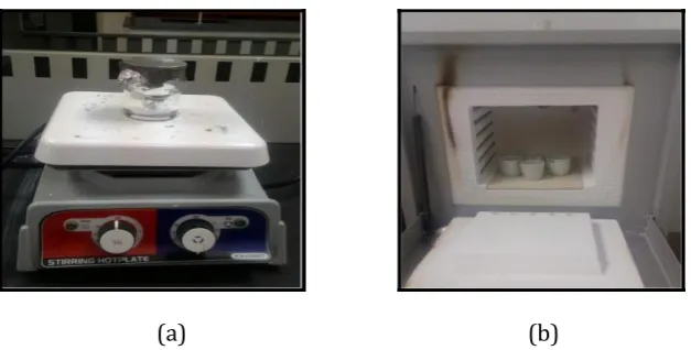
Figure 1. Procedure of (a) stirring process to obtain clear solution and (b) annealing process.
ZnO thin films were prepared by the sol–gel method. As a starting material, zinc acetate dehydrate was used. Isoprophyl alcohol and monoethanolamine (MEA) were used as a solvent and stabiliser, respectively. Zinc acetate dehydrate was dissolved in a mixture of isoprophyl alcohol and MEA solution at room temperature. At the same time, MEA acts as a base and a complexing agent [12]. The molar ratio of MEA to zinc acetate was kept constant at 0.2. The solution was stirred on hotplate stirrer for 2 hours to yield a clear and homogeneous solution as shown in Figure 1(a), which served as a coating solution after cooling to room temperature. The solution was aged for various durations, which were 12 hours, 24 hours, and 48 hours at room temperature. The glass substrates were cleaned with acetone. Film deposition was carried out in air at room temperature. The glass substrates were coated by a dipping process at room temperature after the specific ageing duration of the three samples. The substrates with one
layer of dip coating were then dried and preheated at 200C for 10 minutes in an oven to
189 which was 24 hours. The procedures from coating to drying were repeated for 1, 3, 5, and 7 times for four samples to increase the film thickness. The absorbance, transmittance, and energy band gap of thin film were determined by using UV-Vis. The thickness of thin film was measured by using a profilometer.
3. RESULTS AND DISCUSSION
3.1 Effects of Thickness on Optical Properties of ZnO
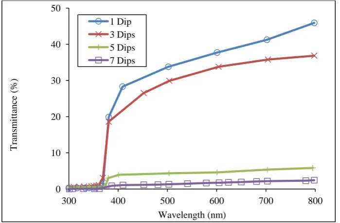
Figure 2. Optical transmittance versus wavelength for ZnO thin film at different layers of coatings.
Figure 2 shows the optical transmittance of ZnO thin film at different thickness in wavelengths ranging from 300 to 800 nm. From the figure, the samples with 1 coating and 3 coatings have a transmittance in a range of 30% to 40%, while the samples with 5 coatings and 7 coatings have a transmittance in a range 3% to 5%. It shows that the thickness of the film decreases the intensity of optical transmittance. The intensity of optical transmittance and transparency of film decreased with the increase in film thickness. The decrease in optical transmittance when the film thickness increases might be due to the presence of native defects and impurities.
According to Myoung et al. [9], as the thickness of film increases, the intensity of emissions
decreases and the intensity of emission depends on the crystalline quality of thin films. Better
crystalline quality results in better optical properties. From a previous study, Kumar et al. [13]
has discovered the effect of film thickness by using SEM images. The surface roughness of the film increased with increasing film thickness. It is due to the formation of larger grains as well as an increase in the porosity of the film. The crystalline quality also decreases when the grain size increases which is due to competition of neighboring crystals with one another for growth.
The optical properties of the thin film describe the nature of the band gap and can be evaluated by extrapolating the linear line part of the curves. The direct band gap of the films were calculated using the relationship as equation (1),
( g)n
hv A hv E
(1)
0 10 20 30 40 50
300 400 500 600 700 800
T
ran
sm
ittan
ce
(
%)
Wavelength (nm) 1 Dip
190
(a) (b)
(c) (d)
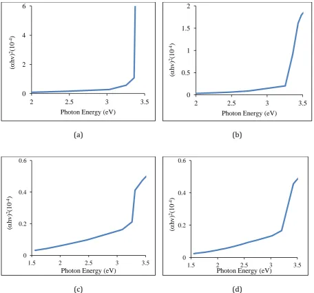
Figure 3. Plot of (αhv)² versus photon energy for direct optical transition of the ZnO thin films of different thickness from (a) 1 dip coated (b) 3 dips coated (c) 5 dips coated (d) 7 dips coated.
where α is the absorption coefficient, A is a constant, hv is the photon energy, n is a constant determining the type of optical transition and Eg is the energy band gap. Figure 3 shows the band gap energy estimated from the absorption edge for ZnO thin film at different thickness. The energy band gap decreased with the increasing of film thickness. The sample that was coated with only 1 dip had a band gap of 3.35 eV, and it decreases to 3.24 eV and 3.20 eV after coating with 3 dips and 5 dips respectively. The lowest energy band gap is ZnO that was coated with 7 dips which is 3.10 eV. This might be due to the variation in lattice defects and stress [13]. The lattice that has compressed is expected to obtain a wide band gap. The grain size is directly related to the compressive stress of film [14]. The stress decreased with the increase of grain size as well as increasing thickness. This is because the compressive stress reduced the density of stress induced defects in the film and also improved the crystal perfection [15].
3.2 Effects of Ageing on Optical Properties of ZnO Thin Films
The initial sol particles with small size were formed through a series of hydration and poly-condensation reactions. The sol will continue to react chemically when the films aged and sol particles agglomerate to become larger. Figure 4 shows the optical transmittance spectra of ZnO
0 2 4 6
2 2.5 3 3.5
( hv) 2(1 0 -4)
Photon Energy (eV)
0 0.5 1 1.5 2
2 2.5 3 3.5
( hv) 2(1 0 -4)
Photon Energy (eV)
0 0.2 0.4 0.6
1.5 2 2.5 3 3.5
( hv) 2(1 0 -4)
Photon Energy (eV)
0 0.2 0.4 0.6
1.5 2 2.5 3 3.5
( hv) 2(1 0 -4)
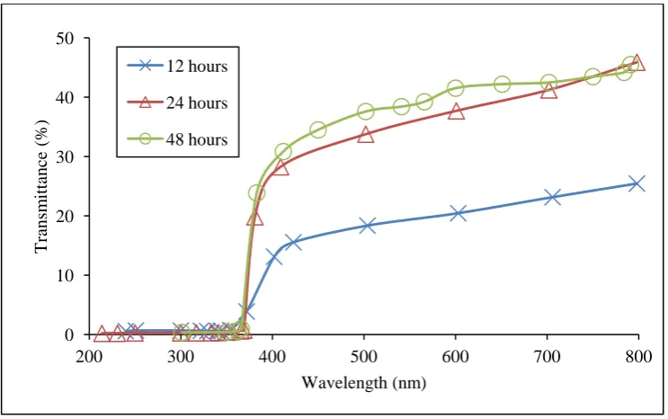
191 thin film at different ageing times in wavelengths ranging from 300 nm to 800 nm. From the figure, the samples which aged for 24 hours and 48 hours have a transmittance in the range of 30% to 40%, while the sample aged for 12 hours has transmittance below 30%. It shows that the ageing process increases the intensity of optical transmittance. The sample aged for 48 hours obtained the highest optical transmittance, while the lowest optical transmittance was obtained when ZnO thin film was aged for 12 hours. This is due to surface scattering and grain boundary scattering that affects the optical transmittance.
Y. Li et al. explained the effect of ageing on the structural properties of ZnO where the surface
roughness gradually decrease and the ZnO grains get more uniform with the increase of ageing time [16]. In relation to Figure 4, it means that the surface of samples aged for 12 hours is relatively rough and its grain boundary is not regular, so the surface scattering and grain boundary scattering are strong. In relation with the previous study, it can be summarized that the surface roughness decreases with increasing ageing time [16], we can relate that the samples that were aged for 24 hours and 48 hours have more uniform grain sizes and have grain boundaries that are clear and regular. As a result, the transmittance of these two samples increased.
Figure 4. Optical transmittance versus wavelength for ZnO thin film at different ageing times.
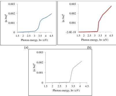
Estimated band gap energy from the absorption edge of the films with different ageing times is shown in Figure 5. The ZnO thin film that aged for 12 hours has a band gap of 3.20 eV, and it increased to 3.29 eV for ZnO that aged for 24 hours. This might be due to the structural homogeneity and crystallinity. As the ageing time increases, the surface roughness are decreased [11] and the lateral size is increased. However, ZnO thin film that aged for 48 hours has a band gap of 3.27 eV. It is shown that the ageing process has little effect on optical properties of ZnO thin film when the ZnO is aged from 24 hours to 48 hours because the refractive index becomes saturated [16] and more difficult to change when ageing time is prolonged up to 24 hours.
0 10 20 30 40 50
200 300 400 500 600 700 800
T
ran
sm
ittan
ce
(
%)
Wavelength (nm) 12 hours
24 hours
192
(a) (b)
Figure 5. Plot of (αhv)² versus photon energy for direct optical transition of the ZnO thin films at different ageing times (a) 12 hours (b) 24 hours and (c) 48 hours.
4. CONCLUSIONS
Thickness of film and ageing time play an important role in determining the optical properties of ZnO thin films. As the layers of thin film were increased, the transmittance reduces due to the larger grain formation and porosity. Films that were coated with 7 layers gave the lowest values of band gap which might be due to the variation in lattice defects and stress. Compressive stress reduced the density of stress in the film and improved the crystal perfection. Meanwhile, when the ageing time was increased from 12 hours to 48 hours, the transmittance spectra increased, showing that the surface roughness gradually decrease and the grain size becomes uniform.
ACKNOWLEDGEMENTS
This project was sponsored by the Kementerian Pendidikan Malaysia (KPM) through grant scheme (USIM/RAGS/FST/36/50215). The author would also like to thank the Photonic Laboratory, Universiti Sains Islam Malaysia for guidance and support.
0 0.001 0.002 0.003
1.5 2 2.5 3 3.5 4 4.5
(
h
v)²
Photon energy, hv (eV)
-2.6E-18 0.001 0.002 0.003
1.5 2 2.5 3 3.5 4 4.5
(
h
v)²
Photon energy, hv (eV)
0 0.001 0.002 0.003
1.5 2 2.5 3 3.5 4 4.5
(
h
v)²
193
REFERENCE
[1] R. A. Rashid, P. S. Menon, S. Shaari. Journal of Nonlinear Optical Physics & Materials. 22, 3
(2013) 1350037.
[2] R. A Rashid, P. S Menon, S Shaari. Optoelectronics and Advanced Materials, Rapid
Communications 7, 11-12 (2013) 835-839.
[3] S. Shaari, A. R. A. Rashid, P. S. Menon, N. Arshad. Advanced Science letters 19, 5 (2013)
1306-1309.
[4] V. Srikant & D. R. Clarke, Journal of Applied Physics 83 (1998) 5447-5451.
[5] P. P. Sahay, S. Tewari, S. Jha, M. Shamsuddin, J. Mater. Sci. 40 (2005) 4791-4793.
[6] S. S. Kumar, P. Venkateswarlu, V. R. Rao & G. N. Rao, International Nano Letters 3, 30
(2013) 1-6.
[7] X. L. Cheng, H. Zhao, L. H. Huo, S. Gao, J. G. Zhao, Sens. Actuators B 102 (2004) 248-252.
[8] J. M. Myoung, W. H. Yoon, D. H. Lee, I. Yun, S. H. Bae & S. Y. Lee, The Japan Society of
Applied Physics 41 (2002) 28-31.
[9] J. Sengupta, R. K. Sahoo, K. K. Bardhan, C. D. Mukherjee. Materials Letters 65 (2011)
2572-2574.
[10] N. C. Ani, S. A. Kamaruddin, N. Nayan, M. Z. Sahdan, Int. J. Nanoelectronics and Materials 8,
(2015) 12-21.
[11] L. Znaidi, T. Touam, D. Vrel, N. Souded, S. B. Yahia, O. Brinza, A. Fischer & A. Boudrioua.
Coatings 3 (2013) 126-139.
[12] Vinod Kumar, Neetu Singh, R., M., Mehra, Avinashi Kapoor, L., P., Purohit, H., C., Swart, Thin
Solid Films 539 (2013) 161-165.
[13] K. Srinivasarao, G. Srinivasarao, K. V. Madhuri, K. Krishna Murthy & P. K. Mukhopadhyay, Indian Journal of Materials Science, 684730 (2013) 1-7.
[14] Yao J. G. Lu,a Z. Z. Ye,b Y. J. Zeng et al. Journal of Applied Physics 100 (2006) 073714.