Design of High Performance Dynamic CMOS
Circuits in Deep Submicron Technology
SALENDRA.GOVINDARAJULU*1, DR. T.JAYACHANDRA PRASAD2
1
Associate Professor, Department of E.C.E, RGMCET, Nandyal, JNTU, A.P-INDIA,
2
Principal, RGMCET, JNTU,A.P-INDIA,
*Corresponding AuthorE-mail address: [email protected]
Abstract
Technology scaling of transistor feature size has provided a remarkable advancement in silicon industry for the last three decades. The demand and popularity of portable electronics is driving designers to strive for small silicon area, higher speeds, low power dissipation and reliability. Compared to static CMOS logic, dynamic logic offers good performance. Wide fan-in logic such as domino circuits is used in high-performance applications. Dynamic domino logic circuits are widely used in modern digital VLSI circuits. These dynamic circuits are often favoured in high performance designs because of the speed advantage offered over static CMOS logic circuits. This paper compares static CMOS, domino (dynamic) logic design implementations of 16-bit Ripple carry adder, 16-bit Comparator and Linear Feedback Shift Register (LFSR) in terms of CMOS layout power consumption, delay, power delay product, area for 65 nm and 45 nm technologies. The techniques are compared by performing detailed transistor simulations on benchmark circuits using Microwind 3 and DSCH3 CMOS layout CAD tools.
Key words: CMOS, Domino logic,Dynamic logic, Layout, Power consumption,Static logic.
I.Introduction
Salendra Govindarajulu et. al. / International Journal of Engineering Science and Technology Vol. 2(7), 2010, 2903-2917
II. Sources of Power Dissipation
The power consumed by CMOS circuits can be classified into two categories:
A. Dynamic Power Dissipation
For a fraction of an instant during the operation of a circuit, both the PMOS and NMOS devices are “on” simultaneously. The duration of the interval depends on the input and output transition (rise and fall) times. During this time, a path exists between VDD and Gnd and a short-circuit current flows.
However, this is not the dominant factor in dynamic power dissipation. The major component of dynamic power dissipation arises from transient switching behaviour of the nodes. Signals in CMOS devices transition back and forth between the two logic levels, resulting in the charging and discharging of parasitic capacitances in the circuit. Dynamic power dissipation is proportional to the square of the supply voltage. In deep sub-micron processes, supply voltages and threshold voltages for MOS transistors are greatly reduced. This, to an extent, reduces the dynamic power dissipation.
B. Static Power Dissipation
This is the power dissipation due to leakage currents which flow through a transistor when no transactions occur and the transistor is in a steady state. Leakage power depends on gate length and oxide thickness. It varies exponentially with threshold voltage and other parameters. Reduction of supply voltages and threshold voltages for MOS transistors, which helps to reduce dynamic power dissipation, becomes disadvantageous in this case. The subthreshold leakage current increases exponentially, thereby increasing static power dissipation.
III. Circuit Techniques
A. Ripple Carry Adder (16 bit):
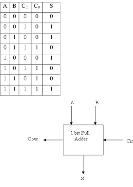
Full adder: A full adder is a logical circuit that performs an addition operation on three binary digits. The full adder produces sum and carry values, which are both binary digits. These are used in multipliers; multipliers are used in digital filters. Fig1 shows Full adder circuit. Table1 shows truth table of full adder.
Fig1: 1-bit Full adder
Table 1: Truth table of 1-bit Full adder
A B Cin C0 S
0 0 0 0 0
0 0 1 0 1
0 1 0 0 1
0 1 1 1 0
1 0 0 0 1
1 0 1 1 0
1 1 0 1 0
1 1 1 1 1
Fig2: Schematic symbol for 1-bit Full adder
Salendra Govindarajulu et. al. / International Journal of Engineering Science and Technology Vol. 2(7), 2010, 2903-2917
Fig3: N bit Ripple carry adder Structure
B. 16 Bit Comparator:
Binary comparators or digital comparators compare digital signals at their input terminals and produces output depending upon the condition of the inputs. For example A is grater, equal or smaller to input B. A comparator is a circuit which compares the relative magnitudes of two numbers. If A and B are two input binary numbers to the comparator, Comparator compares and gives the output as logic 1 when A>=B. Fig4 shows the static comparator circuit. Fig5 is the schematic symbol of 1-bit comparator. Table2 shows the truth table of comparator. Fig6 shows N-bit comparator structure.
Fig4: Schematic symbol of 1bit Comparator
Table2: Truth table of Comparator
Cin Ai Bi Cout Decision
0 0 0 0 A<=B
0 0 1 0 A<B
0 1 0 1 A>B
1 0 0 1 A>B
1 0 1 0 A<=B
1 1 0 1 A>B
Fig5: N bit comparator structure
C. Linear Feed Back Shift Register:
LFSR is a shift register when clocked moves the signal through from one flip flop to next. Some of the outputs are combined in XOR configuration to form feed back mechanism. A LFSR can be formed by performing XOR on the outputs of two or more of the flip flop together and feeding those outputs back into the input of one of the flip flops as shown in Fig.
Salendra Govindarajulu et. al. / International Journal of Engineering Science and Technology Vol. 2(7), 2010, 2903-2917
Fig 7: Structure of Master-Slave D Flip Flop
The initial value of the LFSR is called the SEED. The sequence of values produced by the register is completely determined by its current or previous state likewise, because the register has finite numbers of possible states, it must be eventually enter a repeating cycle. However, a LFSR with a well chosen feed back function can produce a sequence of bits which appears random in nature. The list of bits position that affects the next state is called the tap sequence.
Table3: Pattern Generated by LFSR
Clk Pulse FF1 OUTPUT FF2 OUTPUT FF3 OUTPUT FF4 OUTPUT
The logic hardware of LFSR contains D flipflop, 2 input OR gate, 2 input XOR gate and inverters. The most imp component of LFSR Design is D flip flop.
Applications of LFSR
1. Used in BIST (Built in Self Test).
2. In Cryptography it is used to generate public and private Keys.
3. In Communications for generating Pseudo Random Numbers generation.
IV. Design and Layout Aspects:
Static logic and Dynamic logic (Domino logic) :
The largest difference between static logic and dynamic logic is that in dynamic logic, a clock signal is used. Dynamic logic is over twice as fast as normal logic; it uses only fast N transistors. Static logic is slower because it uses slow P transistors to compute logic. Dynamic logic is harder to work, but if we need the speed there is no other choice. Dynamic logic requires two phases, the first phase is set up phase or pre charge phase, in this phase the output is unconditionally go to high (no matter the values of the inputs A and B).The capacitor which represents the load capacitance of this gate becomes charged. During the evaluation phase, CLK is high. Popular implementation of dynamic logic is domino logic. Domino logic is a CMOS based evaluation of the dynamic logic techniques which are based on the either PMOS or NMOS transistors. It was developed to speed up the circuits. The dynamic gate outputs connect to one inverter, in domino logic. In domino logic, cascade structure consisting of several stages, the evaluation of each stage ripples the next stage evaluation, similar to a domino falling one after the other. Once fallen, the node states cannot return to “1” (until the next clk cycle), just as dominos, once fallen, cannot stand up. The structure is hence called domino CMOS logic. Fig8 shows static implementation of Ripple carry adder. Fig9 shows domino Ripple carry adder. Fig10 shows layout of 16-bit Ripple carry adder with static logic. Fig11 is the layout of bit ripple carry adder with domino logic. Fig12 shows bit static comparator. Fig13 is the domino 16-bit comparator. Fig14 is the layout of static comparator. Fig15 is the layout of domino comparator.
Salendra Govindarajulu et. al. / International Journal of Engineering Science and Technology Vol. 2(7), 2010, 2903-2917
Fig9:16 bit Ripple carry adder (Static logic)
Fig11: Layout of 16bit RC adder (Static logic)
Salendra Govindarajulu et. al. / International Journal of Engineering Science and Technology Vol. 2(7), 2010, 2903-2917
Fig14: 16 bit Domino Comparator
Fig15: Layout of Static Comparator
Fig17: Simulation of Static LFSR
Fig18: Simulation of Domino LFSR
V. Simulation Results
Salendra Govindarajulu et. al. / International Journal of Engineering Science and Technology Vol. 2(7), 2010, 2903-2917
Table4: 16-bit Ripple carry Adder
Techniques Power
(µw)
Delay (ns)
PDP X (10-15)
(Watt-sec)
Area (µm2)
Static
logic
65nm 26 0.365 9.5 5229
45nm 14.4 0.060 0.87 1748
Domino
logic
65nm 14.4 0.105 1.515 5253
45nm 11.9 0.052 0.62 1707
Table5: 16-bit Comparator
Techniques Power
(µw)
Delay (ns)
PDP X (10-15)
(Watt-sec)
Area (µm2)
Static
logic
65nm 43.558 0.105 4.57 2281
45nm 23..980 0.044 1.055 729
Domino
logic
65nm 6.609 0.073 0.4824 1972
45nm 3.821 0.075 0.2865 662
Salendra Govindarajulu et. al. / International Journal of Engineering Science and Technology Vol. 2(7), 2010, 2903-2917
Table6: LFSR
Techniques Power
(µw)
Delay (ns)
PDP X (10-15)
(Watt-sec)
Area (µm2)
NANDGATES 45nm 15.550 0.046 0.7153 307
Static logic 45nm 26.462 0.048 1.270 319
Domino logic 45nm 9.646 0.061 0.588 501
VI. Conclusions
In this project, an attempt has been made to design 2input AND, 2input OR, 2input XOR, D Flip Flop which are the basic building blocks for the benchmark circuits 16 bit Ripple carry adder,16 bit Comparator, Linear Feed Back Register. The proposed circuits have offered an improved performance in power dissipation when compared with standard static circuits. In this work, it can be concluded that 16 bit Ripple carry adder, 16bit Comparator and LFSR can be best implemented using domino logic. In the domino logic for 16 bit Ripple carry adder power delay product at 65nm is 1.515X (10-15) watt-sec, at 45nm 0.68X (10-15) watt-sec., 16 bit comparator power delay product at 65nm is 0.4824X (10-15) watt-sec, at 45nm is 0.2865X (10-15) watt-sec. In the domino logic for LFSR power delay product at 45nm is 0.588X (10-15) watt-sec
References
[1] S. Borkar, “Obeying moore’s law beyond 0.18 micron,” in Proc. IEEE Int. ASIC/SOC Conf., Sept. 2000, pp. 26–31.
[2] R. Ronen et al., “Coming challenges in microarchitecture and architecture,”Proc. IEEE, vol. 89, pp. 325–339, Mar. 2001.
[3] M. T. Bohr, “Nanotechnology goals and Challenges for electronic applications, ”IEEE Trans.Nanotechnol., vol. 1, pp. 56–62, Mar.
2002.
[4] D. J. Frank et al., “Device scaling limits of Si MOSFET’s and their application dependencies,” Proc. IEEE, vol. 89, pp. 259–288,
Mar. 2001.
[5] R. K. Krishnamurty, A. Alvandpour, V. De, and S. Borkar, “High-performance and low-power challenges for sub-70 nm
microprocessor circuits,”in Proc. IEEE Custom Integrated Circuits Conf., May 2002, pp.125–128.
[6] S. Mutoh et al., “1-V power supply high-speed Digital circuit technology with multithreshold- voltage CMOS,” IEEE J. Solid-State
Circuits, vol.30, pp. 847–854, Aug. 1995.
[7] V. Kursun and E. G. Friedman, “Domino logic with dynamic body Biased keeper,” in Proc. Eur. Solid- State Circuits Conf., Sept.
2002, pp.675–678.
[8] “Variable threshold voltage keeper for contention reduction in dynamic circuits,” in Proc. IEEE Int. ASIC/SOC Conf., Sept. 2002,
[9] S. Borkar, Low Power Design Challenges for the Decade, Proceedings of the IEEE/ACM Design Automation Conference, pp. 293-296, June 2001.
[10] P. Srivastava, A. Pua, and L. Welch, .Issues in the Design of Domino Logic Circuits, Proceedings of the IEEE Great Lakes
Symposium on VLSI, pp. 108-112, February 1998.
[11] G. Balamurugan and N. R. Shanbhag, .Energy- efficient Dynamic Circuit Design in the Presence of Crosstalk Noise,. Proceedings of
the IEEE International Symposium on Low Power Electronics and Design, pp. 24-29, August 1999.
[12] S.Govindarajulu, T.Jayachandra Prasad, “Low power,Energy-efficient Domino Logic Circuits”, IJRTE, vol.2, No.7, Nov.2009,
pp.30-33, Academy Publishers, ACEEE, Finland.
[13] S.Govindarajulu, T.Jayachandra Prasad, “Low-Power, High Performance Dual Threshold Voltage CMOS Domino Logic Circuits”,
published in ICRAES, 8th & 9th Jan’2010, pp-109-117,KSR College of Engg., Tiruchengode, India.
[14] S.Govindarajulu, T.Jayachandra Prasad, “Robust, Energy-efficient Reduced Swing Domino Logic Circuits”, IJRTE, vol.3, No.4,
pp.129-133, May.2010, Academy Publishers, ACEEE, Finland, “in Press”
[15] S.Govindarajulu, T.Jayachandra Prasad, “Considerations of Performance Factors in CMOS Designs”, ICED 2008, Dec.1-3 ,Penang,
Malaysia, IEEE Xplore.
[16] S.Govindarajulu, T.Jayachandra Prasad, “,Energy-efficient Reduced swing Domino Logic Circuits in 65 nm Technology”, IJEST, Vol.
2(6), 2010, pp.2248-2257.
[17] S.Govindarajulu, T.Jayachandra Prasad, “,Temperature Variation Insensitivein Energy-efficient CMOS Circuits Design in 65 nm
Technology”, IJEST, Vol. 2(6), 2010, pp. 2140-2147.
Biographical Notes
1
Salendra.Govindarajulu:- He is working as an Associate Professor in the Dept. of Electronics & Communication Engg. at RGMCET, Nandyal, Andhra Pradesh, India. He presented more than 13 International/National Technical Papers. He is a Life Member of ISTE, New Delhi. His interest includes Low Power VLSI CMOS design.
2