ISSN: 2231-5381
http://www.ijettjournal.org
Page 786
Design Optimize Interference Dielectric Edge Filter
Elham Jasim MohammadPhysics Department, Collage of Sciences, Al-Mustansiriyah University, Iraq
Abstract— An Edge filter is a multilayer coating with a
substantial pass-band on either designated side of the stop-band. The Edge filter is meant to have a crisp boundary between wavelength regions that are reflected and those that are transmitted. In this paper, design, optimize, and measurements of an Edge filter is presented. TiO2/SiO2 materials system provides a promising solution for realizing low cost lasers, detectors, and optical modulators operating in the telecommunications, by fabricating these devices on Fusedsilica substrates. An extensive comparison of the response obtained from initial design and the final optimization design is presented. In these study results we demonstrate a dielectric multilayer filter. TiO2 (refractive index n=2.346) and SiO2 (refractive index
n=1.485) edge filter design with a controlled transmission,
reflectivity, absorption, optical admittance, electric field, and dispersion in the wavelength range 300-1000nm.
Keywords— Edge Filter, Long-Pass, Short-Pass, Quarter Wave
Stack, Group Delay, Group Delay Dispersion.
I. INTRODUCTION
Filters in which the primary characteristic is an abrupt change between a region of rejection and a region of transmission are known as edge filters. Edge filters are divided into two main groups, long wave pass (LWP) and short wave pass (SWP). The operation may depend on many different mechanisms and the construction may take a number
of different forms [1]. Edge filters provide a well-defined
transition between reflecting and transmitting regions. Essentially a modified quarter wave stack, the filters use interference effects rather than absorption to isolate their spectral bands. Because Edge filters will shift shorter with an increase in the angle of incidence, they are a good choice for fine-tuning the cut-on/cut-off wavelength, useful for redirecting a particular band of light, provide steeper transition than colour glass filters, and offer coverage over the 400–1000nm range [2]. In long-pass (LP) filter (Fig. 1), the goal is to minimize transmission below a given wavelength and maximize transmission above it.
Fig. 1 Long wave pass Edge filter [2]
These designs are usually based on a quarter wave stack, which has a well-defined transition from reflecting to transmitting. Sometimes absorbing materials are used to increase the optical density of the non-reflecting (rejection) band of the filter. Short-pass Edge filters; used as laser clean-up solutions on the laser source side of the system, attenuate wavelengths to ~ 1.3 wavelength edge. They serve as excellent clean-up filters when there are no laser lines or plasma at shorter wavelengths then the primary line being used. Compared to laser line filters, they provide higher transmission and fully block the laser “tail” on the long wavelength side of the laser line.
In short-pass (SP) filter (Fig. 2), the goal is to minimize transmission above a given wavelength and maximize transmission below it.
Fig. 2 Short wave pass Edge filter [2]
Long-pass Edge filters are designed to transmit wavelengths greater than the cut-on wavelength of the filter. Long-pass Edge filters are used to isolate portions of the spectrum in a variety of industrial or life sciences applications including microscopy or fluorescence instrumentation. Long-pass Edge filters can be used with short-pass Edge filters to create custom band-pass filters. Certain long-pass Edge filters can also be used as cold mirrors to minimize the heat buildup often caused by infrared radiation.
II. QUARTER WAVE STACK INTERFERENCE EDGE FILTERS
ISSN: 2231-5381
http://www.ijettjournal.org
Page 787
effective, approach has been found in the development of entirely new forms of solution of Maxwell’s equations in stratified media [1].
A classical optical stretcher consists of a stack of
layers of thicknesses di and indices of refraction Ni between
an incidence and an exit media of indices of refraction Ninc
and Nex, respectively. To calculate the optical properties, the
ith layers are represented by [3]:
i i i i i i i i i M cos sin sin /
cos (1)
Where: on polarizati p N N on polarizati s N i i i i i i cos / cos 2 (2)
is the pseudoindex of the layer, i(2/)Nidicosi is the
phase shift of the wave inside the layer, i is the angle of
propagation in the layer, and is the wavelength of light in
vacuum.
According to the Snell law Ni , sini is constant. The
pseudoindices and phase shift can be calculated using [4]:
on polarizati p N N on polarizati s N i i i i 2 2 2 2 2 /
(3)
i i
i N d
2 2 2
(4)
The characteristic matrix describing the multilayer is:
1 22 21 12 11 q i i M m m m mM (5)
where q is the number of layers, and the product is taken in
reverse order since the matrices of upper layers must be multiplied on the left. The amplitude reflection and transmission coefficients of the multilayer are [5]:
21 12 22 11 21 12 22 11 m m m m m m m m r ex inc ex inc ex inc ex inc
(6)
21 12 22 11 2 m m m m t ex inc ex inc inc
(7)
Where inc and ex are the pseudoindices of the incidence and
exit media, respectively. The reflectance and transmittance are: 2
*
r rr R .
2 * Re Re Re Re t N N tt N N T inc ex inc ex
(8)
Where, Re is the real part and * denotes the complex
conjugate. The absorptance is simply:A1RT.
When dealing with a rapidly changing signal, such as a pulse train, one also needs to know the dispersive properties of the multilayers. The global phase shifts on reflection and
transmission modulo2 , and r are the angles made by r and
t in the complex plane so that [5]:
r r r r Re Im arctan arg
(9)
t t t t Re Im arctan arg
(10)
Where, Im is the imaginary part and the signs of the numerator
and the denominator must be evaluated separately [5].
The phase shifts do not provide much information about the behaviour of the design. One is usually more interested in the delay introduced when a pulse is reflected or transmitted, the group delay (GD), or in the deformation of a finite bandwidth pulse caused by the variation of GD with the wavelength, the group delay dispersion (GDD). The group delay is defined as the negative of the derivative of the phase response with respect to frequency [6], [7], GD, also known as "Envelope Delay" [8]. Group delay dispersion is a ubiquitous, and often irritating, phenomenon in ultrafast laser labs. When ultrashort pulses propagate through dispersive media, their frequency components emerge at different times due to GDD, causing the resulting pulse to be chirped and stretched and reducing the pulse’s peak power. This effect can be compensated by
using a pulsecompressor, which can introduce negative GDD
[9]. The standard method for computing the GDD is to compute complex reflection coefficients using the transfer matrix technique and then take successive finite difference over frequency [10]. GD and GDD are obtained from the phase using:
d d
GD (11)
2 2 d d
GDD (12)
Where, 2c/is the angular frequency and c is the speed
of light in vacuum. There are analytical formulas to calculate the GD and GDD, but it is impossible to calculate them analytically from the characteristic matrix of a multilayer. The solution appears as a very elegant product of 2 × 2 matrices, each matrix representing a single film. Unfortunately, in spite of the apparent simplicity of the matrices, calculation by hand of the properties of a given multilayer, particularly if there are absorbing layers present and a wide spectral region is involved, is an extremely tedious and time-consuming task. The preferred method of calculation is to use a computer. This makes calculation so rapid and straightforward that it makes little sense to use anything else. The matrix method itself brings many advantages. In the design of a thin-film multilayer, we are required to find an arrangement of layers which will give a performance specified in advance, and this is much more difficult than straightforward calculation of the properties of a given multilayer.
There are two basic multilayer designs that are currently used for Edge filters. One design has the pass-band on the high wavelength side of the stop-band, the other on the low wavelength side. The designs are the following:
Medium/ m L H L 2
2 /Substrate "Low pass"
Medium/ m H L H 2
ISSN: 2231-5381
http://www.ijettjournal.org
Page 788
The designs are illustrated below [11]:
Fig. 3 Edge filter designs [11]
III.RESULTS AND DISCUSSION
It is often difficult, or even impossible, to manually design a filter respecting all the specifications for a given application. However, it is possible to optimize a filter using refinement [12]. In this method, the designer provides a starting design whose properties are sufficiently close to the specifications. Then, an optimization algorithm is used to adjust the thickness of the layers and eventually their index of refraction. In addition to the starting design, the designer must provide targets describing the specifications. The targets can be any property computable from the parameters of the filter; usually, these are the reflection, the transmission, phase properties, or the polarization and angle of incidence. Depending on the application, it may be necessary to define a target at a single wavelength or over a range of wavelengths. In the latter case, the target must in fact be discretized and defined at a finite number of wavelengths.
In this study, we designed Edge filter using Titanium
Dioxide (TiO2) and Silicon Dioxide (SiO2). The structure
composed (21) layers of TiO2 (refractive index n=2.346) and
SiO2 (refractive index n=1.485), wavelength rang
300-1000nm, and design wavelength=550nm has been used in calculations. Fig. 4 and Fig. 5 represent the relationship between the quarter wave stack layers depth and the refractive index for the initial and final filter design.
Fig. 4 Depth versus refractive index for the initial Edge filter design
Fig. 5 Depth versus refractive index for the final Edge filter design
Fig. 6 and Fig. 7 show the phase behave before and after the optimization processe. In order to consider the properties of
the filter, it is common to consider the phase shift as a
function of . The phase change (r()) of the reflected
wave can be developed by using the propagation matrices that are obtained from Maxwell’s equations.
Fig. 6 Phase versus wavelength for the initial Edge filter design
Fig. 7 Phase versus wavelength for the final Edge filter design
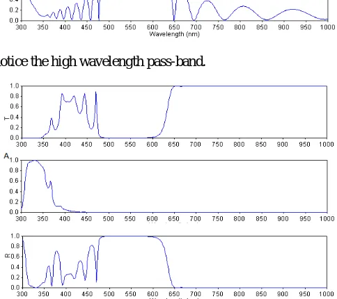
Figs. 8 and Figs. 9 represents the relationship between wavelength with transmission (T), absorption (A), and reflection (R) respectively for the initial design and the final optimized design. After the optimization processes, we can
ISSN: 2231-5381
http://www.ijettjournal.org
Page 789
Figs. 8 Transmission, absorption, and reflection respectively versuswavelength for the initial Edge filter design
Figs. 9 Transmission, absorption, and reflection respectively versus wavelength for the final Edge filter design
Almost as important as the transmitting optical components are to reflect a major portion of the incident light. In the vast majority of cases the sole requirement is that the specular reflectance should be as high as conveniently possible, although, there are specialized applications where not only should the reflectance be high, but also the transmitting and absorption should be extremely low.
Fig. 10 and Fig. 11 show the group delay versus the wavelength. It is clearly seen; the very small oscillations in the group delay are visible over design wavelength 550nm after the optimization process in the final Edge filter design.
Fig. 10Group delay versus wavelength for the initial Edge filter design
Fig. 11Group delay versus wavelength for the final Edge filter design
Fig. 12 and Fig. 13, show the group delay dispersion versus the wavelength. Of course, the same behaviour can be found for the GDD.
Fig. 12Group delay dispersion versus wavelength for the initial Edge filter design
Fig. 13 Group delay dispersion versus wavelength for the final Edge filter design
When thin-film optical coatings are illuminated by light, standing wave patterns form which can exhibit considerable variations in electric field amplitude both in terms of
wavelength and position within the coating. The electric field distribution, Fig. 14 and Fig. 15, profile of electric field intensity for radiation incident on a multilayered system for the Edge filter design, also are plotted in this study.
It can be observed that strong electric field intensity occurred at the first layer and the electric field intensity starts to diminish after it has passed the layer region.
Fig. 14Electric field versus distance from the substrate for the initial Edge filter design
Fig. 15Electric field versus distance from the substrate for the final Edge filter design
The admittance diagram Fig. 16 and Fig. 17 permits a simple technique for assessing these amplitude variations and from them deductions about losses can be made, sometimes with surprising results. In this discussion we limit ourselves to normal incidence.
Fig. 16Optical admittance diagram to real and imaginary part for the initial Edge filter design
Fig. 17Optical admittance diagram to real and imaginary part for the final Edge filter design
ISSN: 2231-5381
http://www.ijettjournal.org
Page 790
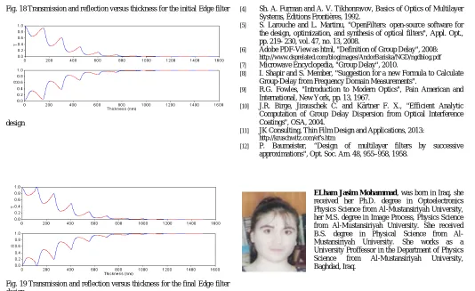
Fig. 18Transmission and reflection versus thickness for the initial Edge filterdesign
Fig. 19Transmission and reflection versus thickness for the final Edge filter design
IV.CONCLUSIONS
In view of the simulation results presented in this study, the main contributions of this research can be summarized below:
The TiO2/SiO2 materials system offers great promise for use
in optoelectronic devices operating in the 300–1000nm wavelength range. Lasers, detectors, and modulators operating in this range are important for telecommunications and optical interconnects. Because Edge filters will shift shorter with an increase in the angle of incidence. The Edge filters used interference effects rather than absorption to isolate their spectral bands. In the case of high reflectors, a combination
of materials with the highest refractive index ratios nh/nl is
usually preferred since the higher the ratio, the higher the theoretical reflectance and bandwidth of standard quarter wave stacks. To design, optimize, or synthesize an Edge filter, we must define targets, single wavelength and spectral reflection, absorption and transmission targets. We can optimize an existing filter using refinement, synthesize a filter using the needle or step methods, or design one using the Fourier transform method.
REFERENCES
[1] H. A. Macleod, Thin-Film Optical Filters, 3rd ed., Institute of Physics Publishing, 2001.
[2] Lot Oriel Gurope, Andover Corporation, Edge Filter Catalog.
[3] F. Abelès, “Recherches sur la propagation des ondes électromagnétiques sinusoïdales dans les milieux stratifiés. Application aux couches minces,” Ann. Phys. (Paris) 5, 1950, 596–640, 706–782.
[4] Sh. A. Furman and A. V. Tikhonravov, Basics of Optics of Multilayer Systems, Éditions Frontières, 1992.
[5] S. Larouche and L. Martinu, "OpenFilters: open-source software for the design, optimization, and synthesis of optical filters", Appl. Opt., pp. 219- 230, vol. 47, no. 13, 2008.
[6] Adobe PDF-View as html, "Definition of Group Delay", 2008:
http://www.dsprelated.com/blogimages/AndorBariska/NGD/ngdblog.pdf
[7] Microwave Encyclopedia, "Group Delay", 2010.
[8] I. Shapir and S. Member, "Suggestion for a new Formula to Calculate Group-Delay from Frequency Domain Measurements".
[9] R.G. Fowles, "Introduction to Modern Optics", Pain American and International, New York, pp. 13, 1967.
[10] J.R. Birge, Jirauschek C. and Kärtner F. X., "Efficient Analytic Computation of Group Delay Dispersion from Optical Interference Coatings", OSA, 2004.
[11] JK Consulting, Thin Film Design and Applications, 2013:
http://kruschwitz.com/ef's.htm
[12] P. Baumeister, “Design of multilayer filters by successive approximations", Opt. Soc. Am. 48, 955–958, 1958.
![Fig. 2 Short wave pass Edge filter [2]](https://thumb-us.123doks.com/thumbv2/123dok_us/8644599.1725337/1.595.63.253.578.695/fig-short-wave-pass-edge-filter.webp)