Ensuring minimum duration of transient processes in
switched voltage regulators with digital control
Oleg V. Nepomnyashchiy
1, *, Yuri V. Krasnobaev
1, Aleksey P. Yablonsky
1, Vyacheslav V. Potekhin
2,
and Natalia J. Sirotinina
11 School of Space and Information Technologies, Siberian Federal University, Svobodny pr. 79, 660041, Krasnoyarsk, Russia
2Higher School Cyber-Physical and Control Systems, Peter the Great St. Petersburg Polytechnic University, Grazhdansky Pr. 28, 195220, St. Petersburg, Russia
Abstract
This paper describes a solution suggested to minimize the finite transient duration of a switched voltage regulator (SVR) for step changes in load current. SVR control laws aimed at minimizing the transient time are synthesized, and the microprocessor-based architecture and operating algorithms of the control system are designed. The prototype of the SVR digital control unit is implemented on the field-programmable gate array integrated circuit Cyclone III EP3C120F780 using the NIOS II soft-processor core. Embedded software is developed to calculate the control pulse duration for power switches in accordance with the synthesized control laws taking into account the feedback loop signal. A case study of the prototype shows that it provides the duration of transients caused by a load current step change, equal to 3-4 conversion periods at the frequency of 120 kHz. It confirms the suitability of the developed models, algorithms and control laws for ensuring the minimum transient duration.
*
Corresponding author. Email: [email protected]
1. Introduction
**Electric and radio equipment requires stable power supply with low voltage deviations in stationary and dynamic operating modes. Requirements to power supply quality, including voltage stability, are regulated by such industry
**
Co-funded by the Erasmus+ programme of the European Union: Joint project Capacity Building in the field of Higher Education 573545-EPP-1-2016-1-DE-EPPKA2-CBHE-JP “Applied curricula in space exploration and intelligent robotic systems”.
The European Commission support for the production of this publication does not constitute an endorsement of the contents which reflects the views only of the authors, and the Commission cannot be held responsible for any use which may be made of the information contained therein.
branch standards as National Aeronautics and Space Administration (NASA), European Space Agency (ESA) and European Cooperation for Space Standardization (ECSS) electrical power supply standards [1]. Voltage stabilization is carried out by switching voltage regulators (SVRs) [2, 3]. Power quality assurance is especially difficult for systems with multiple power sources and/or energy consumers [4]. To enhance voltage stability, efficient SVR control laws are being developed [5–7]. These control laws are usually implemented by a pulse width modulation (PWM)-based controller. Generally, PWM controllers are manufactured in the form of application-specific integrated circuits (ASICs) [8–10]. In addition to SVR control and voltage stability assurance, PWM controllers can perform a wide range of service functions, such as temperature control, circuit overload protection, etc. [11, 12].
Keywords: switching voltage regulator, SVR, control law, transient time, adjustable components of state variables, digital control loop, field-programmable gate array, FPGA.
Received on 20 December 2018, accepted on 14 October 2019, published on 16 October 2019
Copyright © 2019 Oleg V. Nepomnyashchiy et al, licensed to EAI. This is an open access article distributed under the terms of the Creative Commons Attribution licence (http://creativecommons.org/licenses/by/3.0/), which permits unlimited use, distribution and reproduction in any medium so long as the original work is properly cited.
2. Problem statement
Requirements to power supply quality, including voltage stability, are becoming increasingly stringent. One of the most promising ways to meet them is to increase the performance of SVR, which allows us to reduce output voltage deviations for dynamic modes of operation. This is possible through developing new, more effective control laws. However, implementing an improved control algorithm with the use of existing series-produced PWM controllers is usually impossible due to mismatch of an internal controller structure with the new control law. For this purpose, small-scale integrated circuits and discrete components can be used, but this will decrease the reliability and increase the intrinsic power consumption of the SVR control unit, as well as its mass and size. Such negative changes in the characteristics of SVR are unacceptable.
The most appropriate and relevant to modern approaches should be considered the implementation of the SVR control unit based on a microprocessor platform with statically and dynamically reconfigurable architecture. Such a system can be developed as a “system-on-a-chip” on the base of ASIC, or partially or wholly field-programmable integrated circuit with an embedded microprocessor core. Reconfigurable microprocessor platforms allow performing both different algorithms of the SVR control and additional functions of SVR self-diagnostics, telemetry, etc. In addition, the proposed approach improves power supply system reliability in critical applications by including more than one SVR and allows implementing maximum power tracking algorithms for renewable energy sources, etc. [13, 14].
Of particular interest is a promising method for the synthesis of SVR control laws, described in [15], because it ensures high performance in output voltage stabilization. The proposed method includes:
Representation of power circuits of SVR with PWM control in the mode of small deviations by a relevant pulse-amplitude model for describing adjustable components of the process.
Synthesis of a control law using polynomial equations for designing pulse-amplitude modulation (PAM) systems [16].
Implementation of the designed control law in a SVR taking PWM features into account.
The proposed method allows designing a control law that provides the minimum transient time in a step-down SVR. The schematic diagram of such a step-down SVR, or buck converter, is shown in Figure 1. It is based on the conventional SVR structure [17]. The difference is that the control unit (CU) is implemented usin a digital integrated circuit with an embedded microprocessor core.
Figure 1.The schematic diagram of the buck converter
3. Control law synthesis
It is proposed to use the SVR control law synthesized on the base of described above method [15] as optimal in performance, and the SVR implementing this control law is to be called a high-performance SVR.
By adjustable components of the process, we mean deviations of variable parameters of the SVR from their values in the stationary mode, which are caused by an increase in the current pulse duration tp.adj relative to the
stationary duration tp.fix.
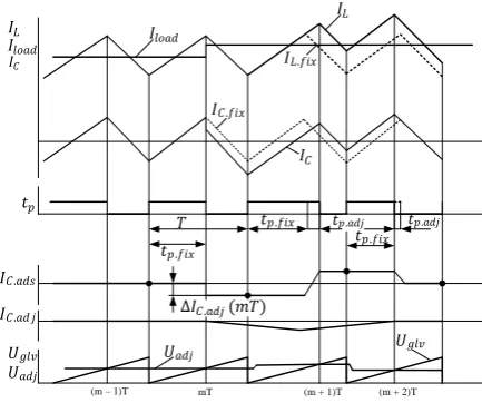
Let us consider selecting an adjustable component on the example of timing diagrams of the buck converter.
Figure 2 presents variations with time of the load current
Iload, the inductor current IL and its stationary IL.fix
component, the output capacitor current IC and its
components: stationary IC.fix and adjustable IC.adj, the
adjustable component of the output capacitor voltage UC.adj,
the conversion period T, the pulse width tp and its
components: stationary tp.fix and adjustable tp.adj, and
sawtooth voltage of the PWM Uglv.
(m – 1)T mT (m + 1)T (m + 2)T
𝐼𝐿 𝐼𝑙𝑜𝑎𝑑 𝐼𝐶
𝐼𝑙𝑜𝑎𝑑
𝐼𝐿
𝐼𝐿.𝑓𝑖𝑥
𝐼𝐶.𝑓𝑖𝑥
𝐼𝐶
𝑡𝑝
𝑇 𝑡𝑝.𝑓𝑖𝑥
𝑡𝑝.𝑓𝑖𝑥
𝑡𝑝.𝑓𝑖𝑥 𝑡𝑝.𝑎𝑑𝑗
𝑈𝑎𝑑𝑗 𝑈𝑔𝑙𝑣 𝐼𝐶.𝑎𝑑𝑠
𝐼𝐶.𝑎𝑑 𝑗
𝑈𝑔𝑙𝑣 𝑈𝑎𝑑𝑗
∆𝐼𝐶.𝑎𝑑𝑗(𝑚𝑇)
𝑡𝑝.𝑎𝑑𝑗
Figure 2.Timing diagrams of the buck converter
(stationary) duration of control pulses tp.fix of the adjusting
element. The second is due to increment of the control pulse duration tp by the amount of tp.adj relative to the stationary
duration tp.fix. Useful information about the control process is
only contained in adjustable components. In case of small deviations of the control pulse duration, the following condition is met: tp.adj <<T, where T is the commutation
cycle duration.
In a system utilizing PWM, the adjustable component is given by voltage pulses uL.p(t) with duration tp.adj(t), that
affect on the inductor from the adjusting element. To pass from PWM to PAM, they are replaced by δ-functions, which are equivalent in terms of the volt-second “area”. It is acceptable in case of small deviations.
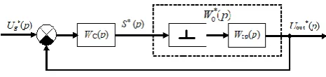
In [18], it is shown that the influence of the load conductance and the inductor internal resistance can be neglected for pulse amplitude SVR model in the case of use the optimal in performance control law. This allows us to represent a pulse-amplitude SVR model as connected an ideal pulse element and elements with transfer functions
1/pL and 1/pС in series (Figure 3).
The adjustable voltage component on the buck converter filter input represents bipolar pulses with amplitude uL.adj(t).
The pulse width tp.adj(t) is equal to the deviation of the pulse
width tp(t) from its stationary value tp.fix. This determines the
input signal of an ideal pulse element for the adjustable components of the pulse-amplitude modulation for the buck converter as:
)
(
)
(
)
(
t
u
.adj.at
t
p.adjt
s
L .Equation (1) corresponds to the proposed pulse amplitude buck converter model:
)
(
)
(
)
(
*adj
.
t
s
t
t
u
L
, (1)where δ*(t) is a sequence of δ-functions with the period T, described by the following expression:
1 *
) ( ) (
m
mT t
t .
PWM-regulation for adjustable components in the field of lattice function transforms is determined by the equation:
) ( ) ( )
( * *
0 *
out p W pS p
U , (2)
where Uout*(p) and S*(p) are lattice function transforms for
adjustable components the output voltage and the control signal respectively; W0*(p) is the discrete transfer function
determined by the transfer function of the continuous part
Wcp(p) [15].
Only the adjustable components of the state variables carry useful information about the pulse-width control process. The constant component does not contain such information, and the pulsation of variable states is an information disturbance. This means that control laws for
SVR should be synthesized on the basis of the expression (2) which describes the process of pulse-width control using adjustable components. Pulsations of state variables should be taken into account when implementing the control law.
Transformation of the pulse-width regulation to the amplitude-pulse regulation in the neighborhood of a stationary mode allows applying a well-developed mathematical apparatus of the PAM [15] for the analysis and synthesis of SVR with PWM control and to develop pulse-based control laws.
The block diagram of the designed pulse system is shown in Figure 3.
Figure 3.The block diagram of the synthesized pulse system
To synthesize the optimal in performance control law for the SVR, we use the third polynomial equation of synthesis [16]. This equation provides for synthesis of the discrete transfer function WC(p) for a feedforward compensator
according to the condition of the minimum finite duration of processes in a closed system depending on external influences and in case of the deviation of the feedforward compensator parameters from calculated values. It ensures the practical feasibility of WC(p) .
) e (1 )
( )
( * 0 1
C2 * C1
pT
d d p W p
W , (3)
where:
2 F 1 0
1
T dd ,
LC
1
2 F
,
L and C are the inductance and the capacitance of the output filter respectively.
4. Developed control methods of the
switched voltage regulator
The control unit for a SVR with PWM control have been designed in accordance with the synthesized transfer function (3), taking specifics of pulse-width modulation into account. Two solutions are considered [15]. The first solution is control depending on instantaneous values of state variables. It suggests preliminary studying relationships between the stationary pulsation and the increment of duration of control pulse tp.adj(t), formed by the
the next step) [18]. A study of this solution proves achieving the transient time of 3–4 conversion periods, which is close to the theoretical limit of 2 periods for a second-order system with pulse-amplitude modulation [18]. At the same time, the study shows a significant static error of stabilization in the output SVR voltage. This is due to the fact that the gain of the feedback loop:
) /(
1 2
F 1
0 d T
d ,
defined by expression (3), is obtained through parameters of the SVR power circuit. Therefore, its increase leads to decrease in performance [19]. In this case, astatism of the output voltage is provided by introducing a second integrating voltage feedback loop [20].
Thus, the input of the pulse-width modulator is the following:
)
(
)
(
)
(
intint.M
t
u
t
u
t
u
d
.
(4)
It is the sum of two signals. The first, ud(t), provides
dynamical properties of the SVR. It is produced by the feedforward compensator according to equation (3). The second, uint(t), provides zero offset of the SVR output
voltage. It is obtained by integrating the error signal e(t) of the SVR output voltage:
1 0
p
int
(
)
(
)
U
t
dt
t
e
K
t
u
, (5)where e(t) = uout(t) – U0, uout(t) is the SVR output voltage,
U0 is the reference voltage, Kp << 4Kopt / (2rcC + T), where
Kopt is the feedback gain factor that determines SVR
dynamic properties, rc is the internal resistance of the output filter capacitor, C is the capacitance of the output filter capacitor.
The second solution is based on extracting adjustable components of SVR state variables at the beginning of a commutation cycle by special sample-and-hold elements. In the case of SVR implementation using microprocessor platform, this approach is preferable considering that it suggests the single-time sampling of signals at the beginning of each commutation cycle. In comparison, the first solution requires multiple analog-to-digital conversions of information signals. According to the second solution, the PWM input signal, which describes dynamic properties of the SVR, is described by the following equation:
)
(
)
)
1
((
)
(
mT
U
m
T
U
mT
U
d
d
d , (6)and its increment by the commutation cycle T is defined as follows:
2
(
)
((
1
)
)
T
)
(
2 .adj .adjpwm in
T
m
U
mT
U
K
U
LC
mT
U
d
c
c
, (7)where Uin is the SVR input voltage. The first difference of
the SVR output voltage is determined as:
)
)
1
((
)
(
)
(
c.adj c.adjc.adj
mT
U
mT
U
m
T
U
, (8)The PWM gain factor is described by the following equation: M
U
T
mT
U
t
K
pwm
t.adj
in.pwm(
)
, (9)where Δtc.adj is the increment of the control pulse duration,
ΔUin.M(mT) is the increment of the PVM input signal,
UMis the amplitude of the PWM sawtooth voltage [19].
Existing microprocessor technologies allow implementing the second approach to the SVR design [20], in correspondence with the optimal in performance control law and with the use of an integrating voltage feedback loop under control of the digital PWM controller.
5. Minimization of transient time
For the considered solution, minimization of the transient time is reduced to calculating the input signal of the PWM controller and producing through this signal the actual width-modulated pulse control signal for the SVR power switch, performed by a microprocessor unit. The PWM input signal is calculated using expression (10), which is obtained from equation (4) taking into account the discrete nature of signal processing:
)
(
)
(
)
(
intin.M
mT
U
mT
U
mT
U
d
. (10)The signal Ud(mT) that determines SVR dynamic
properties is defined by equations (6)–(8). The first difference of the adjustable component of the SVR output voltage, which is described by equation (8), can be described by the following expression:
)
)
1
((
)
(
)
(
C.adj
mT
E
mT
E
m
T
U
, (11)where E(mT) is the discrete value of the loop error signal on the SVR output voltage, which is determined taking into account (5) as follows:
0 out
(
)
)
(
mT
U
mT
U
E
. (12)This replacement is acceptable because the SVR output voltage, presented as:
)
(
)
(
)
(
)
(
C.adj fix rippleout
mT
U
mT
U
mT
U
mT
U
,contains besides the adjustable component UC.adj(mT) the
fixed component Ufix(mT) and the ripple component
Therefore, when calculating the first difference UC.adj(mT)
using equation (11) and taking into account (12), the fixed component Ufix(mT), the output voltage ripple Uripple(mT)
and reference voltage U0, biased in relation to each other by
the commutation cycle T, are mutually subtracted. The signal Uint(mT) providing astatism of the SVR, can be
calculated by the expression:
)
(
)
(
1 р
int
mT
K
E
kT
U
m
k
, (13)It is distinct from the expression (5) taking into account the replacement of integration by summation.
Information signals necessary for the SVR control, are the voltage at the input and output of the SVR. Their sampling is carried out at the time instants mT. Digital conversion and further calculations take the time interval ts
<< T. In the considered case, the SVR power switch performs modulating the leading edge of a control pulse. The delay in determining the control pulse width of the SVR power switch does not have a significant effect on the calculation result, because calculations are performed at the time interval when the power switch is turned off.
Figure 4 presents the block diagram of the signal processing sequence performed by the microprocessor control system.
Figure 4.The block diagram of the signal processing sequence performed by the microprocessor control
system
Analog-to-digital converters ADC1 and ADC2 provide sampling and analog to digital conversion of the SVR input voltage uin(t) and the output voltage uout(t) at time instants
mT, i.e. define signals Uin(mT) and Uout(mT). Then,
computing unit C1 calculates the first difference for the adjustable component of the output voltage ΔUC.adj(mT)
according to (11) in the vicinity of the time point mT. Thereafter, computing unit C2 defines the signal Ud(mT),
which is responsible for SVR dynamic properties. Computing unit C3 defines the signal Uint(mT) which is
responsible for astatism of the SVR output voltage. Then, the adder calculates Uin.pwm(mT) by summing Ud(mT) and
Uint(mT) according to (10). After that, the PVM controller
defines the control pulse width tc.adj according to the equation tc.adj = KM Vin.pm defined by (9). The obtained width
will take effect during the next time period to time instants mT. The microprocessor control system synchronizes the falling edge of a control pulse with the time instant (m+1)T.
6. Implementation of designed control
laws and control algorithms
To confirm the theoretical results obtained, a prototype of the buck converter with digital control is implemented. It is designed in accordance with the structure presented in Figure 1. The functional diagram of the buck converter is depicted in Figure 5.
Figure 5.The functional diagram of the buck converter prototype
The power part (1) of the prototype includes:
Power switch, made on the MOSFET transistor VT. Closing diode VD1.
Input and output capacitors Cin and Cout.
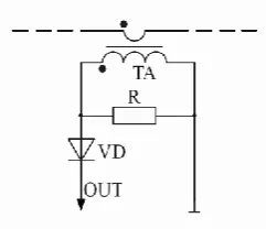
Induction L and inductor current sensor (2) (Figure 6), implemented on current transformers TA1 and TA2 and load resistor R1.
The control unit prototype includes:
Voltage dividers (3) consisting of resistors R4, R5 and R1, R3.
Driver (4) to control the transistor VT.
Control automaton (5) on the base of Field Programmable Gate Array (FPGA) circuit Altera Cyclone III EP3C120F780 with integrated NIOS-II processor core.
Analog-to-digital converter (6) based on max1308. Analog integrator (7) and adder (8), implemented on an
operational amplifier. Reference voltage source (9).
Figure 6.Inductor current sensor
The buck converter prototype has the following main characteristics:
the buck converter output voltage uout= 28 V,
the input voltage uout varies from 40 V to 110 V,
the conversion frequency fc = 120 kHz,
the capacitance of the input Cin and output Cout filter
capacitors is 1000 μF ;
the inductance L = 180μH at the 1.5A inductor current and L = 120 μH at the 4 A inductor current.
The prototype is designed to determine dynamic characteristics close to the maximum possible, in combination with the output voltage astatism in static operating modes.
The control unit implements the algorithm of generating control signals for the buck converter power switch at the microprogram level. The algorithm is presented in Figure 7. In calculations, the average inductance is assumed 150 µH.
Embedded software for the microprocessor control unit has been developed. At the first stage, the software time delay of the first sample is introduced. This is performed in order to finish transients of digital and analog modules and reach operating mode of power supply electronic components. During this delay, the variables are initialized, the control subsystems are set, the system constants are defined, such as the initial value of the control signal pulse duration (tc.st), the pulse width, the modulation period of the
signal, the value of the reference voltage U0, etc.
Hereinafter, time interval lines are implemented at the hardware-software level using programmable timer-counters.
At the end of the software delay, a sync signal is received from the main timer. After receiving the sync signal, the signal for controlling power switches is generated. In the first program cycle, the width of the power switch control pulse tc.adj (MT) is set by the initial value tc.st, which is
necessary for starting the buck converter. Then, input signals are synchronously converted by ADC 1 and 2 (Figure 4) into the digital format of the values Uin(mT) and Uout(mT)
respectively. ADCs operate in parallel; the beginning of the conversion is synchronized. The ADCs perform conversion during a small offset interval τ <0.25T, i.e. during the first quarter of the period. There may be some temporary mismatch in the completion of the conversion steps. However, difference of digitization time is insignificant, of
the order of 10-12 seconds. This does not affect results in the calculation time intervals and is synchronized when receiving data from the ADC by the microprocessor unit in the direct memory access mode.
At the end of the measurements, correction values are calculated. Next, the duration of power switch control pulse is calculated for the next program cycle, corresponding to the time instant mT + 1. The calculation is performed in accordance with the formula (10) by the expression:
tc.adj(mT) = KpwmUin.pwm(mT)
In more detail, the algorithm of the developed embedded software is shown in Figure 7.
А Startup of PWM generation with pulse
duration tc.adj(mT) Initialization of variables
ΔUc.adj(mT)=0, ΔUd(mT)=0, ΔUint(mT)=0,
tc.adj(mT)=tc.st
Analog to digital conversion of buck converter voltages Uin(mT) and Uout(mT)
Calculation of loop error signal E(mT)=Uout(mT)-U0
START
Specifying of constant parameters Kpwm, Kp, T, U0, tc.st
А
Calculation of adjustable component for output
voltage Uc.adj(mT)
Calculation of Ud(mT)
Calculation of Uint(mT)
Waiting for stop signal
END Waiting for
synchronization
Calculation of PWM input signal Uin(mT)=Ud(mT)+Uint(mt)
Calculation of control pulse duration tc.adj(mT)=KpwmUin.pwm(mT)
True False
False
True
Figure 7. The algorithm of the embedded software for buck converter controller
7. Experimental results
Figure 8.The functional diagram of the test facility
The test facility includes: buck converter prototype (1), power supply with adjustable supply voltage range from 40 V to 110 V (2), current sensor in the form of a resistive Rsh
shunt with a resistance of 0.2 Ohm (3), a load unit consisting from constantly connected and periodically switched resistors (4) and a four-channel oscilloscope (5).
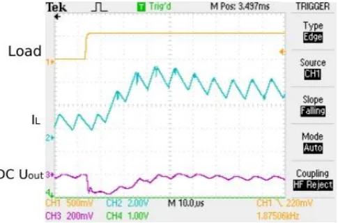
The results of studying the buck converter prototype are shown in Figures 9–11.
Figure 9. Step change in output current
Figure 10. Step decrease in output current
Figure 11. Step increase in output current
In all figures the first signal from the top (Load) represents the load current change in 2.5 A/div scale, the second signal (IL) represents the inductor current in 2 A/div
scale, the third signal (DC Uout) is the adjustable component of the buck converter output voltage in 0.2 V/div scale. The fixed component of a load current is shown in the figure partly. The timescale is 100 μs/div. Processes that comprise two commutation cycles of the step load current change are shown in Figure 9. The constant component of the load current is 1.4 A, and the step load current increment is 2.8 A. Figure 3 proves out that the control process meets the zero offset requirements because the output voltage returns to its initial value after finishing the transient process. Further tests confirm the absence of the output voltage offset even if the buck converter input voltage varies in the range mentioned above. Figure 10 and Figure 11 show step load current decrease and step load current increase processes on a large scale respectively. The transient time is approximately 5–6 commutation cycles for the step load current decrease process (fig. 6) that is close to the minimum possible transient time. The transient time is approximately 6–8 commutation cycles for the step load current increase process (figure 7). Increase in the transient time relative to its minimum value is explained by the determined limitation of the maximum control pulse width at 0.75T. The reason of limiting the pulse width is the need for an additional time interval for demagnetization of the inductor current sensor based on the transformer, analog-to-digital converting informational signals and calculating the width of the buck converter control pulse.
8. Conclusion
SVR power circuits in the mode of small input voltage deviations by a relevant pulse-amplitude model for describing adjustable components of the process. The synthesis of SVR control laws is performed using polynomial equations for designing PAM control and implementation of the designed control law in the SVR considering PWM features. This method allows designing a control law that provides the minimum transient time in a step-down switched voltage regulator. A microprocessor platform with statically and dynamically reconfigurable architecture is suggested as the most relevant hardware platform for the SVR control unit. The prototype of the buck converter with digital control unit is implemented using a FPGA circuit with an integrated processor core.
Experimental studying the prototype proves the efficiency of the proposed method. In case of a step change of the load current, the described solution provides the minimum finite duration of transients equal to 5-6 conversion periods, approaching the lowest theoretically possible limit. The experiments show that single sampling and analog-to-digital conversion of input signals, and calculating correction values of the control pulse during a commutation cycle T, releases significant time resources of the microprocessor control unit. The released time resource can be utilized to diagnose the buck converter or to distribute the load current between several buck converters operating in parallel for the common load and other maintenance functions, which is an additional advantage of the proposed buck converter control method. The use of switching power supply with digital control unit implemented by means of high-performance microprocessor systems provides significant strategic advantages over analog systems.
References
[1] ECSS-E-ST-20C [Electrical and electronic (31 July 2008)]. European Cooperation for Space Standardization. Available http://ecss.nl/standard/ecss-e-st-20c-electrical-and-electronic
[2] Tyunin S.S., Kabirov V.A., Semenov V.D., Kobzev A.V. Direct Buck Converter with Zero Voltage Transition and PWM Control (ZVT-PWM). 13th International scientific-technical conference on actual problems of electronic instrument engineering (APEIE) – Novosibirsk, 2016, vol. 1, no. 3, pp. 29–35.
[3] Krasnobaev Yu.V., Pozharkova I.N. Determination of output impedance permissible values of an autonomous power supply system. Bulletin of the Siberian Aerospace University – Krasnoyarsk, 2007, vol 3, pp. 91–96. In Rus.
[4] Borodin D.B., Kabirov V.A., Vintonyak N.P., Semenov V.D., Shurygin Y.A. Direct Boost Converter with Zero Voltage Transition and PWM Control (ZVT-PWM). 13th International scientific-technical conference on actual problems of electronic instrument engineering (APEIE) – Novosibirsk, 2016, vol. 1, no. 3, pp. 22–28.
[5] Tanovitskiy Y., Kobzev G., Savin D. Minimizing the Duration of the Transient Processes in a Buck Converter with Pulse Width Modulation and Inert Output Filter. Procedia Technology, 2014, no.18, pp. 6–13.
[6] Cheng P., Vasic M., Garcia O., Oliver J.A., Alou P., Cobos J.A. Minimum Time Control for Multiphase Buck Converter: Analysis and Application. IEEE Transactions on Power Electronics, 2014, no. 29/2, pp. 958–967. [7] Nejabatkhah F., Danyali S., Hosseini S.H., Sabahi M.,
Niapour S.M. Modeling and Control of a New Three-Input DC–DC Boost Converter for Hybrid PV/FC/Battery Power System. IEEE Transactions on Power Electronics, 2012, no. 27/5, pp. 2309–2324. [8] PWM controllers Texas Instruments [PWM controllers
of Texas Instruments]. Available at: https:// www.compel.ru/lib/ne/2007/3/5-shim-kontrolleryi-texas-instruments, 2018.
[9] Shtrapenin G. New generation of integrated circuits. National Semiconductor for switching power supplies. Components and technologies. 2007, no. 8, pp. 114–118. In Rus.
[10] Analog world of Maxim. New power microcircuits. Maxim Integrated Products – Moscow, 2014, no.3, 60 p. In Rus.
[11] Wen Y., Trescasesr O. DC–DC Converter With Digital Adaptive Slope Control in Auxiliary Phase for Optimal Transient Response and Improved Efficiency. IEEE Transactions on Power Electronics, 2012, no. 27/7, pp. 3396–3409.
[12] Zhou G., Xu J., Jin Y. Improved digital peak current predictive control for switching DC–DC converters. IET Power Electronics, 2011, no. 4/2, pp. 227–234.
[13] Mahdavikhah B., Jain P., Prodic A. Digitally controlled multi-phase buck-converter with merged capacitive attenuator. Twenty-Seventh Annual IEEE Applied Power Electronics Conference and Exposition (APEC) – Orlando, 2012, pp. 1083-1087.
[14] Vintonyak N.P., Fedotov V.A., Semenov V.D. Technique of designing microcontroller software for high-speed control systems. Reports of TUSUR. 2015, no.2, pp. 175–179. In Rus.
[15] Soustin B.P., Ivanchura V.I., Chernyshev A.I., Islyaev Sh.N. Power supply systems for space vehicles. Siberian Publishing Company – Novosibirsk, 1994, 318 p. In Rus. [16] Tsypkin Ya.Z. Theory of linear impulse systems. physical and mathematical and technical literature – Moscow, 1963, 968 p. In Rus.
[17] S. Maniktala, Switching Power Supplies A to Z, second ed., Newnes, Elsevier, 2012, pp. 53–59
[18] Manakov A.V., Ivanchura V.I., Soustin B.P. Synthesis and investigation of a high-speed switching voltage regulators with PWM. Technical electrodynamics. 1987, no. 1, pp. 43–51.
[19] Krasnobaev Yu.V. Methodology of synthesis of laws and structures of converter control devices. University proceedings. Ser. Instrument engineering. 2004, vol. 47, no. 4, pp. 39–48.