1
Modeling of the wave electromagnetic processes in the
microwave microelectronic material
V.V. Pivnev
1,*, P.Y. Voloshchenko
2and Y.P. Voloshchenko
31 Southern Federal University, 105/42 Bolshaya Sadovaya Str., Rostov-on-Don, 344006, Russia 2 Southern Federal University, 105/42 Bolshaya Sadovaya Str., Rostov-on-Don, 344006, Russia 3 Southern Federal University, 105/42 Bolshaya Sadovaya Str., Rostov-on-Don, 344006, Russia
Abstract
This is the abstract. This is the abstract. This is the abstract. This is the abstract. This is the abstract. This is the abstract. This is the abstract. In article the nonlinear electromagnetic processes in electronic material, formed by the ordered structure of discrete electronic devices of a gigabyte and terahertz ranges are considered. Based on structural and technological design of real microwave integrated circuit fragment, the analytical expressions for model describing the processes of accumulation and exchange, dissipations and redistribution of oscillatory energy caused by signal composition in interconnections of the ordered microwave structure are synthesized. The results of a research of disturbance intensity variation in uniform electromagnetic field of integrated circuit are shown on the example of a quarter-wave equivalent two-wire transmission line loaded with the semiconductor device with tunable negative conductivity
Keywords: microwave integrated circuit, negatron, microwave electronic device, ordered structure of electronic devices, amplitude-dependent nonlinear element, microstrip transmission line, conductive interconnection, wireless interconnection, electromagnetic energy distribution, coherent electronics technology.
Received on 13 November 2017, accepted on 9 December 2017, published on 13 December 2017
Copyright © 2017 Pivnev V.V et al., licensed to EAI. This is an open access article distributed under the terms of the Creative Commons Attribution licence (http://creativecommons.org/licenses/by/3.0/), which permits unlimited use, distribution and reproduction in any medium so long as the original work is properly cited.
doi: 10.4108/eai.13-12-2017.153471
*Corresponding author. Email:[email protected]
1. Introduction
It is known that microwave high-power integrated circuits with negatrons - avalanche transit time diodes and resonant tunneling diode can be considered as a material medium that transforms the electromagnetic field energy. In this case, the combination of electronic devices is defined by a dielectric and magnetic permittivity, electrical resistance, characteristic impedance, wave front phase speed and mobility of free charge carriers, depending on the exposure intensity. It reflects in general the inertial and nonlinear electric properties of integrated circuit regions made from various materials and dynamic abilities of substances used for manufacturing in terms of the electromagnetism macroscopic theory. Besides that,
the coherent accumulation and exchange, dissipation and redistribution of oscillatory energy, interference and diffraction effects of electromagnetic waves along conductive and wireless interconnections takes place in such system. At the same time, this conception ignores inner structure of integrated circuit constructed from isolating, directing and resistive parts, direct current input metal electrodes and signal outputs. That is why in giga and terahertz range the constructive synthesis of integrated circuit of any type that provides energy consumption optimization should be implemented on the basis of interdisciplinary engineering approach that considers the special aspects of microwave electronic device material modeling [1]. When calculating effectiveness factor for this IC it is impossible to use static methods that are based on the principle of superposition, a priori concepts of discrete energy state
On Energy Web
EAI Endorsed Transactions on Energy Web and Information Technology
2 and indistinguishability of interacting electronic devices, that are forming the microelectronics composite material.
At the same time it is lawful to study the ordered structure of microwave electronic devices as an electronic wave chain with generalized and full currents circulating in its branches and contours. Then the initial estimation of oscillatory energy redistribution in system is reduced to composing and solving the simultaneous equations of controlled electric balance and multimode operation stability by methods of complex amplitudes and equivalent sinusoids. As related unknown parameters of integrated circuit model, the constant and alternating voltage and current of the resistive-negatron nonlinear elements that simulate correlatively working avalanche transit time and resonant tunneling diodes are used.
2. The model of construction part of
high-power integrated circuit basic
element
To study the one-tones compositions in material of microwave integrated circuits we will use graphic and analytical operators of circuit model accurately devised in [1; 2].
The figure 1 shows the model of construction part of high-power integrated circuit basic element consisted from two discrete avalanche transit time diodes operating in three centimeter wave rage, placed on the opposite sides of circuit. Distributed strip line connects diodes with each other and with the load, oscillation energy and direct current sources. In this microwave structure, for the transmission line that is loaded with the semiconductor devices, it is impossible to define a single value for instantaneous amplitude-dependent initial and transient boundary conditions that define the limits and the integration constant.
This is the body text with indent. This is the body text with indent. This is the body text with indent. This is the body text with indent. This is the body text with indent. This is the body text with indent. This is the body text with indent. This is the body text with indent. This is the body text with indent. This is the body text with indent. This is the body text with indent. This is the body text with indent. -- In this circumstances two adjacent discrete semiconductor devices together with conductors are considered as a basic element of the wave synergistic system, substituted by the equivalent one-dimensional electronic circuit. The paths of convection and induced currents circulation are modeled by uniform feeder line segment of arbitrary length l with no distributed losses and dispersion, shunted by the bipolar resistance-negatron nonlinear element. The inertial and nonlinear monochromatic response of fragment is observed on its input and output terminals which corresponds the "virtual" boundaries of the circuit. The nonlinear element is an active dipole with indefinite internal resistance, that radiates electromagnetic energy in an unlimited or a specified frequency range. It replaces the electronic
obstacle in the microwave transmission line and can be both primary and secondary signal source in a one-dimensional electrical circuit. Negatrons represent a partial compensation of the semiconductor device energy losses and the reverse transmission of oscillating energy between them at the arbitrary alternating current frequency.
To observe the mechanism of single tone signal overlapping in the artificial material the methods of equivalent sine waves, complex amplitudes, nodal-pairs, oscillatory characteristic and harmonic linearization of semiconductor devices parameters are used [1; 2]. Then, to get the analytical relation for cluster electromagnetic energy distribution in the dielectric and semiconductor environment (figure 1) the correlation of only the first voltage and current harmonics of the nonlinear element are considered. This approach is caused by lack of analytical solutions to differential equations describing ultrafast periodic electromagnetic processes and interrelated characteristics of circuit electronic branches.
Figure 1. The model of construction part of high-power integrated circuit basic element
2.1. The solution to wave equation of
electronic circuit with the distributed
parameters
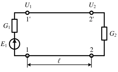
Figure 2 shows the topology of inertial conductive and wireless connections between electronic devices using the equivalent one-dimensional scheme of structure of wave and nonlinear electric processes between electronic heterogeneity. Consider that primary monochromatic signal impact characterized by the voltage source E1 and
frequency is located at the beginning of line with distributed parameters and produces in it the complex
. 1
U
amplitude. Then the branch that connects scheme output terminals (2-2'), we consider as a passive or active
nonlinear element depending on the operating-point position and as a coherent secondary source of alternating current.
EAI Endorsed Transactions on Energy Web and Information Technology
3
ℓ
E
1G
1U
1U
21'
1
2
2'
G
2Figure 2. The equivalent circuit of conductive and wireless connections between electronic devices in
material of microwave integrated circuit
Let's write down the solution to wave equation of electronic circuit with the distributed parameters as a sum of standing waves [1; 2]:
)]Z (U [U jI ) (U U ) (E U . sin
cos 2 2 1 0
1 2 1
1 , (1)
where =l=2πl/λ - interconnection electrical length, λ - electromagnetic oscillations wavelength which defines a space period of ordered material structure. The ratio (1) in general symbolical form determines the allocation of microwave electronic devices in knots or antinodes of electric field by variation of its impedance. On outputs 1-1' and 2-2' (figure 2) of graphic operator the boundary conditions are satisfied: G1=Gн1=Y0,
I2[U2(U1)]=U2{Gн2+Ge2[U2(U1)]}=U2G2, Gн2>0,
Ge2(U2)<0. Here variables: U2, I2=Iн2+Ie2[U2(U1)] – voltage and current amplitudes at connections points 2-2'
of nonlinear elements;
γ
jβ
.
– propagation factor ofelectromagnetic field perturbation in the zero-loss uniform transmission line (– phase coefficient); Y0=1/Z0, l – its characteristic admittance and geometrical length;
Gн1=Y0, Gн2, Ge2(U2) - frequency-independent conductivity of a source and a "useful" load simulated by negatron and resistor. Using a formula (1) and Tellegen's theorem we receive the equation that describes the diffraction and interference of one-tones along the transmission line and electromagnetic wave front in the material medium of superfast integrated circuit:
0 2 2 2 2 2 2 2 2 2 2 2 1 2 2 2
1,U ) U U [cos θ g (U )sin θ] 0, g G Y
F(U .
(2) The parameter is directly proportional to the size l and the external impact frequency . When =n (n=1,2,3…)
the equality
2 2 2 1
,U
U
is true, and when =(n – 1/2) theratio
U
U
[g
(U
)]
2 2 2 2 2 2 2
1
is characterized by totalreduced conductivity
g
(U
)
2 2 2
2 of nonlinear element
which can be greater or less than 1. Constant n considers the range discretization of a characteristic oscillations and an ambiguity of an electric states in modeling multimode circuit. Therefore, the expressions (1), (2) allow to analyze symbolically the amplitude-dependent features of
electronic obstacles in wave scale (i.e. relatively to the values λ и Y0 without defining the parameter values of its elements in metric system of units). Approximate the nonlinear element active impedance characteristic with
the relation
g
(U
)
g
g
(
1
νU
)
2 2 02 e 2 н 2 2
2
using theharmonic linearization method [1; 2], where
2 2 02
2
g
U
g
ν
< 0 – nonlinearity factor, g02=gн2–ge02
–small-signal conductivity of resistive-negatron element. Define the variables x= , y= . Then from expression (2) we receive the cubic expression which has one real solution:
02 02 2
3 2 3
3 2 3
3 ) ( 2 ) ( e e н x x x x x x g g g p q q p q q y
x , (3)
0 ) θ 1 ( θ 3 3 ) ( 2 2 2 02 2 2 02 2 02 02 2 02 02
2
e e e e н e e н x g ctg y g ctg g g g g g g q , 0 3 1 θ 3 2 02 02 2 2 02 e e н e x g g g g ctg p
,
as the discriminant
0
3
2
q
xp
xD
at any parameter value y in the parameter range 0<ge02/gн2<1. The analytical operator (3) describes the composition of waves, characterizes voltage U2, current I2=U2G2 and an operating point of nonlinear element in the stationary mode of electronic device. Therefore, due to the electromagnetic wave diffraction, the extremum disposition of electric field potential in the end of a long interconnection varies when adjusting the common field perturbation intensity in the open structure of integrated circuit material. Besides, the equivalent line loaded with the active impedor can coincidently increase alternating voltage U2 and current I2 amplitude due to electric energy
transformation by the electronic circuit.
Characteristics of quarter-wave segment of transmission line with a nonlinear element
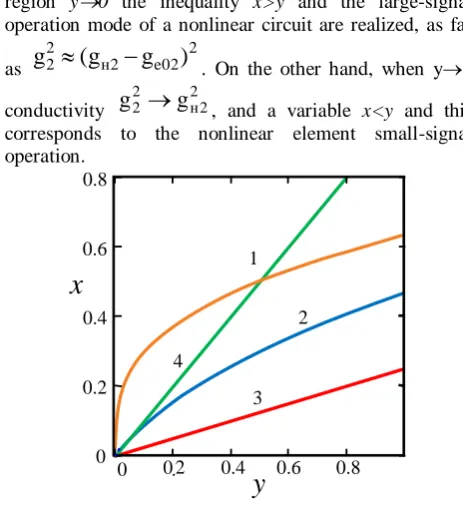
Let's consider nonlinear inertial processes in basic element of the analog integrated circuit using as the example the quarter-wave transformer with a nonlinear element when adjusting negatron negative conductivity. It is known that the usage of transmission line segment with the length =/2 optimizes the electric energy transfer in idealized circuits with the distributed parameters [1 – 6]. On the other hand, such test case of space structure of composite microwave material gives an opportunity to investigate analytically how the interference affects on "virtual" edges of integrated circuit in an explicit form, to verify the model of nonlinear addition and signal subtraction.
In figure 3. the characteristic x=f(y) of quarter-wave transmission line segment with nonlinear element is given. It illustrates the wave summation result in the circuit section 2-2' (figure 1) for gн2=2 of "useful" load and several values of negatron small-signal conductivity: curve 1 – ge02=2, 2 – ge02=1, 3 – ge02=0. In this case
function
[
(
)]
2 2
x
g
x
y
. Therefore in the perturbedEAI Endorsed Transactions on Energy Web and Information Technology
4 region y0 the inequality x>y and the large-signal operation mode of a nonlinear circuit are realized, as far
as
2 02 e 2 н 2
2
(
g
g
)
g
. On the other hand, when y1
conductivity
2 2 н 2
2
g
g
, and a variable x<y and thiscorresponds to the nonlinear element small-signal operation.
0 0.2 0.4 0.6 0.8 0
0.2 0.4 0.6 0.8
2
3 1
y
x
4
Figure 2. Disturbance intensity variation in uniform electromagnetic field of equivalent two-wire transmission line loaded with the semiconductor
device
Test graph 4 in figure 3 shows that the squares of amplitudes are equal x=y in the input and output of the line with =. For the active impedor impedance value
ge02=0 the variable
2 2 н
g
y
x
is a linear function of intensity source E1 and inversely proportional to a
conductivity square. In case of small-signal compensation of resistive "useful" losses by a negatron (gн2-ge02=0), the nonlinear parameters transformation of such system in wave scale is illustrated by formulas:
3 2 н 3
02 e 2
2
2
(U
)
g
y
g
y
g
. At the same time, the oscillatory energy transfer in a microwave multimode circuit is unidirectional and it operates in running wave mode with any value of
g
н2
1
that is greater than oneand when the production is
g
y
g
νU
1
2 1 02 e 2
н
.Variation of voltage source E1 results in disposition of
maximum and minimum of voltage standing wave in the end of the line and nonlinear element operating point. At the same time, when condition ge02=gн2=1 is true which corresponds to traditional optimum "useful" load and placing electronic obstacle in regular infinite line, the
dependence of variables
3
y
x
is described by a power function. In this case the resultant wave voltage amplitude on line outputs 2-2' is limited by a total conductivity
3 2
1 3
2 2
2
(U
)
y
νU
g
of an electronic circuit.
Thus, the boundary conditions in the beginning and in the end of the studied one-dimensional electronic circuit, microwave electric field extremum position relative to electronic device depend on primary source intensity and interference effect in artificial material. Therefore under the invariable influence the circuit output signal level can be increased and reduced by adjusting in an appropriate way the amplitude-dependent nonlinear element response of a secondary coherent wave source. "Matching" of electronic circuit and long line parameters is provided by adjusting negatron nonlinear characteristics. At the same time, placing of avalanche transit time diodes and resonant tunneling diodes in a voltage standing wave minimum or a maximum corresponds to its essentially different operating points and the collective interaction steady modes of contiguously-allocated diodes integrated by coherent electronics technology. Therefore the authors consider that at the first step in modeling of gigahertz and terahertz integrated circuits for various applications as a composite material of synergetic system it is impossible to calculate analytically or numerically the instantaneous state for particular electronic device when assuming that conditions for "small disturbance" or "weak nonlinearity" are valid.
Acknowledgements.
This work was supported by Russia's Southern Federal University grant №ВнГр-07/2017-15: «Development of theoretical foundations and creation methods of intelligent multivariable control systems for generating processes, transportation, distribution and consumption of energy».
References
[1] Voloshchenko P.Yu., Voloshchenko Yu.P., Methodology of the mathematical simulation of nonlinear wave and oscillating electrical processes in the articles of coherent radio-, micro- and nano-electronics, SFedU, Taganrog, 2013.
[2] Voloshchenko P.Yu., Voloshchenko Yu.P., The bases of system modeling of high-speed devices integration electric structure, SFedU, Rostov-on-Don, 2014.
[3] Voloshchenko P.Yu., Voloshchenko Yu.P., Vavilov V.G., Chernobrovy V.S., Symbolic analysis of electric structure of material for analog and digital coherent electronics products, in: Abstracts and Schedule of the 2015 International Conference on “Physics and Mechanics of New Materials and Their Applications”, SFedU, Rostov-on-Don, 2015.
[4] Voloshchenko P.Yu., Voloshchenko Yu.P., Vavilov V.G., Zaycev A.I., Mathematical modeling of electromagnetic wave processes in materials of high-speed integrated circuits, in: Abstracts and Schedule of the 2015 International Conference on “Physics and Mechanics of New Materials and Their Applications”, SFedU, Rostov-on-Don, 2015.
[5] Pivnev V.V., Basan S.N. Some questions about equivalent circuit synthesis and nonlinear electrical circuit implementation with the specified properties in the electronic simulation tasks: Applied Mechanics and
EAI Endorsed Transactions on Energy Web and Information Technology
5 Materials Vols. 670-671 (2014) P.1454-1457. - Access: http://www.scientific.net/AMM.670-671. 1454.
[6] Pivnev V.V., Basan S.N., Voloshchenko Y.P., The application of approximation characteristics non-linear resistor implement the required current-voltage characteristics, in: Proceedings of the International Conference on Advances in Energy, Environment and Chemical engineering., Рart of series: Advances in Engineering Research., Volume: 23, Atlantis Press, Amsterdam-Beijing-Paris, 2015.
EAI Endorsed Transactions on Energy Web and Information Technology