Study of surface modifications for improved selected metal
(II-VI) semiconductor based devices.
BLOMFIELD, Christopher James.
Available from Sheffield Hallam University Research Archive (SHURA) at:
http://shura.shu.ac.uk/19362/
This document is the author deposited version. You are advised to consult the publisher's version if you wish to cite from it.
Published version
BLOMFIELD, Christopher James. (1995). Study of surface modifications for improved selected metal (II-VI) semiconductor based devices. Doctoral, Sheffield Hallam University (United Kingdom)..
Copyright and re-use policy
See http://shura.shu.ac.uk/information.html
SHEFFIELD HALL AM UNIVERSITY LIBRARY CITY CAMPUS POND STREET
SHEFFIELD SI 1W8
z s l $ l % - i b . s r
3 - "7 •
S j ^ r
i
6
: s ^
ProQuest Number: 10694243
All rights reserved
INFORMATION TO ALL USERS
The quality of this reproduction is dependent upon the quality of the copy submitted.
In the unlikely event that the author did not send a com plete manuscript and there are missing pages, these will be noted. Also, if material had to be removed,
a note will indicate the deletion.
uest
ProQuest 10694243
Published by ProQuest LLC(2017). Copyright of the Dissertation is held by the Author.
All rights reserved.
This work is protected against unauthorized copying under Title 17, United States C ode Microform Edition © ProQuest LLC.
ProQuest LLC.
789 East Eisenhower Parkway P.O. Box 1346
Study of Surface Modifications for Improved Selected
Metal (II-VI) Semiconductor Based Devices.
Christopher James Blomfield BSc
A thesis submitted in partial fulfilment of the requirements of Sheffield Hallam University for the degree of Doctor of Philosophy.
August 1995
Abstract.
Metal-semiconductor contacts are of fundamental importance to the operation of all semiconductor devices. There are many competing theories of Schottky barrier formation but as yet no quantitative predictive model exists to adequately explain metal-semiconductor interfaces. The II-VI compound semiconductors CdTe, CdS and ZnSe have recently come to the fore with the advent of high efficiency photovoltaic cells and short wavelength light emitters. Major problems still exist however in forming metal contacts to these materials with the desired properties. This work presents results which make a significant contribution to the theory of metal/II-VI interface behaviour in terms of Schottky barriers to n-type CdTe, CdS and ZnSe.
Predominantly aqueous based wet chemical etchants were applied to the surfaces of CdTe, CdS and ZnSe which were subsequently characterised by X-ray photoelectron spectroscopy. The ionic nature of these II-VI compounds meant that they behaved as insoluble salts of strong bases and weak acids. Acid etchants induced a stoichiometric excess of semiconductor anion at the surface which appeared to be predominantly in the elemental or hydrogenated state. Alkaline etchants conversely induced a stoichiometric excess of semiconductor cation at the surface which appeared to be in an oxidised state.
Metal contacts were vacuum-evaporated onto these etched surfaces and characterised by current-voltage and capacitance-voltage techniques. The surface preparation was found to have a clear influence upon the electrical properties of Schottky barriers formed to etched surfaces. Reducing the native surface oxide produced near ideal Schottky diodes. All three materials exhibited the formation of several discrete Schottky barriers; for Au/n-CdTe (|)b = 0.64, 0.725, 0.96 and 1.10 ± 0.02 eV, for Au/n- CdS (|)b = 0.86 and 0.96 ± 0.02 eV. An extended study of Au, Ag and Sb contacts to n- ZnSe/n+-GaAs substrates again revealed the formation of several discrete Schottky barriers largely independent of the metal used; for Au/n-ZnSe (j)b = 0.90, 1.2, 1.45 and 1.65 ± 0.04 eV, for Ag/n-ZnSe (|)b = 1.2 and 1.45 ± 0.04 eV and for Sb/n-ZnSe (|)b = 1.45, 1.65, 1.8 and 2.1 ± 0.04 eV.
Acknowledgements
I would first of all like to acknowledge the help and support of my supervisors, Dr IM Dharmadasa, Dr J Young and Dr J Haigh for their advice and guidance offered throughout the course of this study. I also owe many thanks to the technical staff of the Materials Research Institute, particularly Messrs G. Gregory and K. Blake for help and assistance with all matters regarding the Microlab. I am also in gratitude to Dr C Scott at the University of Hull and Dr R Coratger at the LOE-CNRS Toulouse for help and co-operation with DLTS and BEEM experiments respectively. Prof BC Cavenett and Dr K Prior at Heriot-Watt University kindly supplied a number of the ZnSe samples used within this study.
I would like to acknowledge the financial assistance of the Higher Education Funding Council for funding the research and the British Vacuum Council and the Institute of Materials Carnegie Award for funding my attendance at the ICMM '95 Barcelona.
Last but not least I have to thank my family for their continued support throughout my time in higher education, Sophie for putting up with me while writing up and the boys at 157 for all the good times.
"Any smoothly functioning technology will have the appearance of magic"
Contents.
Chapter 1. Introduction.
1.1 Introduction to metal-semiconductor interfaces 1
1.1.2 Schottky-Mott theory. 2
1.2 Physical properties and applications of II-VI compound semiconductors 3
1.2.1 Applications of ZnSe. 7
1.2.2 Applications of CdTe and CdS 9
1.3 Aims and objectives. 12
1.4 Approach. 13
Chapter 2 Models and theories of Schottky barriers.
2.1 Introduction. 15
2.2 Models of Schottky barrier formation. 15
2.2.1 The Bardeen model. 16
2.2.2 The linear model 17
2.2.3 The effective work function model 18
2.2.4 Models of Fermi level pinning 19
2.2.5 The pinch-off model 23
2.2.6 Summary of models 24
2.3 Current transport mechanisms 24
2.3.1 Thermionic emission 25
2.4 Capacitance of a Schottky barrier 35
2.4.1 Deviations from the ideal capacitance 36
3.1 Introduction 39
3.2 Experimental surface studies of CdTe, CdS and ZnSe. 39
3.2.1 Surface studies of CdTe 39
3.2.2 Surface studies of CdS 49
3.2.3 Surface studies of ZnSe 55
3.3 Properties of metal contacts to II-VI compounds 57
3.3.1 Introduction 57
3.3.2 Metal contacts to CdTe 57
3.3.3 Metal contacts to CdS 64
3.3.4 Metal contacts to ZnSe 66
3.4 Deep levels and defects in II-VI compounds 72
3.4.1 Introduction 72
3.4.2 Deep levels in CdTe 73
3.4.3 Deep levels in CdS 76
3.4.4 Deep levels in ZnSe 77
3.5 Summary of deep levels in CdTe, CdS and ZnSe 80
Chapter 4 Experimental techniques.
4.1 Introduction 81
4.2 Surface analysis 81
4.2.1 X-ray photoelectron spectroscopy 81
4.3 Wet chemical etching and contact fabrication 91
4.3.1 Introduction 91
4.3.2 Semiconductor samples 91
4.3.3. Wet chemical etching 91
4.3.4 Metal contact formation 92
4.4.1 Current-voltage (I-V) characterisation 93
4.4.2 Capacitance-voltage (C-V) characterisation 97
4.5 Deep level transient spectroscopy 99
4.5.1 Theory 99
4.5.2 Instrumentation 102
4.6 Ballistic electron emission microscopy 103
4.6.1 Introduction 103
4.6.2 Theory 103
4.6.3 Instrum* entation 106
Chapter 5 Surface studies of II-VI compounds
5.1 Introduction
5.2 X-ray photoelectron spectroscopic surface analysis of CdTe, CdS
5.2.1 CdTe 5.2.2 CdS 5.2.3 ZnSe
5.4 Summary of surface etching of CdTe, CdS and ZnSe
Chapter 6 Electrical characterisation of contacts to etched surfaces.
6.1 Introduction 141
6.2 Au/n-CdTe 141
6.2.1 Non-ideal contacts 141
6.2.2 Ideal contacts 145
6.2.3 C-V characteristics 149
6.2.4 Ageing of contacts 151
6.2.5 Deep level transient spectroscopy of Au/n-CdTe 155
108 and ZnSe
108 110
120
6.3 Au/n-CdS 156
6.3.1 Non-ideal contacts 156
6.3.2 Ideal contacts 160
6.3.2.1 Summary of ideal contacts 160
6.3.3 C-V characteristics 163
6.3.4 Ageing of Au/n-CdS 165
6.4 Metal contacts to ZnSe 170
6.4.1 Non-ideal contacts 170
6.4.2 Ideal contacts; Au/n-ZnSe 172
6.4.3 Ideal contacts, Ag/n-ZnSe 174
6.4.4 Ideal contacts, Sb/n-ZnSe 177
6.4.5 Summary of electrical measurements of metal/n-ZnSe devices 181
6.4.6 Deep level transient spectroscopy of Au/n-ZnSe 182
6.4.7 Ballistic electron emission microscopy studies of Au/n-ZnSe 184
Chapter 7 Discussion of results
7.1 Introduction 191
7.2 Schottky barrier heights in he context of present theories 192
7.2.1 Schottky model 192
7.2.2 Linear model 194
7.2.3 Effective work function model 195
7.2.4 Models of Fermi level pinning 196
7.3 Thermodynamics of metal-semiconductor interfaces 199
7.3.1 Introduction 199
7.3.2 Heat of reaction 200
7.3.3 Heat of formation 201
7.3.4 Summary 203
7.4.1 CdTe
7.4.2 CdS and ZnSe
7.4.3 Native defects and the Schottky barrier
204
206 208
Chapter 8 Conclusions and recommendations for future work.
8.1 Wet chemical etching
8.2 Electrical characterisation
8.3 Future work
8.4 Contribution to device technology
References
Appendix 1
A1.1 Refereed publications. A1.2 Conferences attended
212
213 215 217
219
i i n i u u u ^ u u n .
Chapter 1
Introduction.______________________________________
1.1 Introduction to metal-semiconductor interfaces.
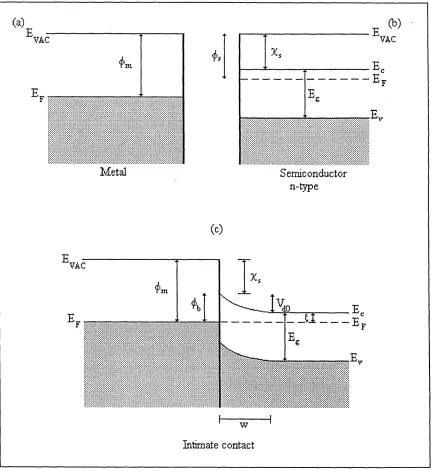
Metal-semiconductor contacts are of fundamental importance to the operation of virtually all semiconductor devices. Decades of research effort have been expended investigating the fundamental physics of such systems but as yet no unifying theory exists to unambiguously explain their behaviour. Often the metal contact is required to provide a gateway for electrons to and from the outside world, such contacts are of low resistance over a large range of electric fields, ideally obeying Ohm's law. Alternatively, the metal- semiconductor contact can form the active region of a specific device. In this instance the contact usually behaves in an asymmetric manner allowing preferential current flow in one direction, the metal-semiconductor system is said to be a rectifier. Many processes of contact formation are often based on empirically derived recipes rather than a thorough understanding of the underlying chemistry and physics. Although device dimensions have decreased by several orders of magnitude over the last three decades there is still uncertainty in producing metal contacts with the desired properties. Such factors now limit the progression to true nanoscale microelectronics. A general lack of understanding of the metal-semiconductor interface for many materials has meant that these materials have as yet not reached their full potential.
Models of metal-semiconductor contact behaviour have evolved in parallel with advances made in analytical methods. Early theories were based upon macroscopic a.c. and d.c. transport measurements. With the development of ultra high vacuum surface analysis came the facility to directly observe the emerging metal contact as sub-monolayers of metal were deposited onto the clean semiconductor surface. Such techniques yielded a wealth of
mii uuuuuon.
new experimental evidence which was followed in turn by new theoretical models bom out of ever increasing computer power.
1.1.2 The Schottky-Mott theory.
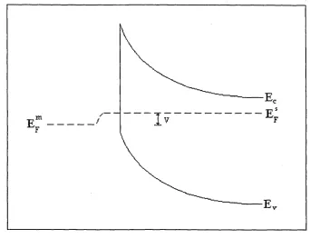
The earliest theoretical attempts to explain the behaviour of metal-semiconductor systems were made almost simultaneously by Mott(1938) and Schottky(1938). Both hypothesised the formation of a potential barrier due to charge transfer at the interface between the metal and the semiconductor. Mott suggested that the difference in work functions of a semiconductor (or salt in his terminology) and a metal, induced a space charge region (which we now refer to as a depletion region) with a linear electrostatic potential. Schottky, on the other hand supposed that the space charge region had a constant density of charged impurities (ionised dopants) and that the electrostatic potential varied quadratically. The Schottky model was largely accepted, the potential barrier at the interface subsequently taking his name. The magnitude of the Schottky barrier (|)b, is the parameter responsible for the so called "ohmic" or "rectifying" nature of the metal contact. Figure 1.1 shows how a Schottky barrier may form when a metal and a semiconductor, of work functions <|)m and (|)s respectively are brought into intimate contact (in this case (|)m > <))s, which is the most common case). Thermodynamic considerations dictate that the Fermi levels (EF) of both materials must coincide, this in turn produces a transfer of electrons from the conduction band (Ec) of the semiconductor to the metal. The result of electron transfer is a build-up of negative charge at the surface of the metal. This charge is contained within a narrow surface region penetrating < 0.5 A into the metal known as the Thomas-Fermi screening distance, Rhoderick and Williams (1988). An equal but opposite charge must exist within the semiconductor, this charge in an n-type semiconductor consists of uncompensated donors created by receding conduction electrons. The charge in the semiconductor is distributed over a much larger distance due to the lower conductivity, a region then exists depleted of conduction electrons known as
lllll UUU^LiUll.
(a)
VAC
m
lllll!!!!!!
Metal Semiconductor
n-type
(b)
VAC
(c)
VAC
m
W
[image:14.621.74.505.31.502.2]Intimate contact
Figure 1.1 A schematic energy band diagram of a metal, (a) of work function (|)m and an n- type semiconductor, (b) of work function (J)s. A Schottky barrier is formed when the two
are brought into intimate contact (c). xs is the electron affinity of the semiconductor and £,
is the difference between the bottom of the conduction band and the Fermi level. Vd0 is the zero bias band bending.
X i l l l V U U V l l U l l .
the depletion region, of width w. The rearrangement of the charge carriers induces band bending in the conduction and valance bands of the semiconductor which in turn produces the potential or Schottky barrier. From figure 1.1 it is clear that the Schottky barrier
height, <j)b, measured from EF is related to <j)m and the semiconductor electron affinity, %s,
by the following expression;
</>>=<!>.-x,
(i i)
The Schottky-Mott theories of barrier formation and hence equation (1.1) were based upon the notion of a perfect intimate contact between the metal and the semiconductor, in many cases such a situation is not possible. Many reported barrier heights did not reflect the linear relationship with <j)m predicted by equation (1.1). Such observations prompted Bardeen (1947) to suggest a model of Schottky barrier formation where the level of charge distribution and hence band bending and barrier height were dependent upon the occupancy of surface states present at a thin interfacial layer between the metal and semiconductor. These surface states in sufficient quantities were said to possess a charge neutrality level (t>0 which acted to pin EF. The equation for Schottky barrier height could then be modified to the so called Bardeen limit;
</>> = E„ - fa (1-2)
(|)0 is generally measured upwards from the valence band (Ev). The origin of surface states and the exact mechanism of EF pinning have been the source of much debate within the literature. Heine (1965) first suggested that these states were metal induced gap states (MIGS) due to exponentially decaying wave functions of the metal adatoms. The role of
defects created by the metal overlayer was investigated by Spicer et al (1979) and
lllll UUUC11UI1.
incorporated into the unified defect model (UDM). Disorder at the interface producing disorder induced gap states (DIGS) was a mechanism proposed more recently by Hasegawa and Ohno (1986) to explain observed barrier heights. Other models have received much attention which focus not on the pinning of EF but on the chemistry of the interface. Freeouf and Woodall (1981) suggested that the work function of the metal <|)m, may be modified to an effective work function (|)eff which would then replace (|)m in
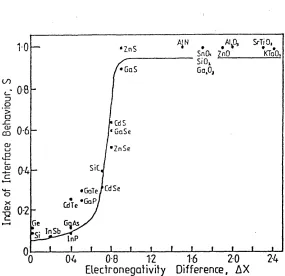
equation (1.1). Kurtin et al (1969) derived a parameter defined as the index of interface
behaviour S, being the difference in electronegativity of two constituents of the semiconductor compound. When S = 1 the barrier height obeyed the Schottky limit and when S= 0 the barrier followed the Bardeen limit. Models of this nature were able to explain the behaviour of many systems but were more qualitative than quantitative.
There have been many attempts to explain the potential barrier between the metal and the semiconductor since Mott and Schottky's original propositions. Many of these theories will be expanded upon in the following chapter and later tested against the results obtained here. In a recent review on the subject of metal-semiconductor interfaces Williams (1991) concluded that a number of processes including chemical reactions, MIGS, defects, interface bonding and crystallography, and interdiffusion may all contribute to the Schottky barrier formation. Similarly, Brillson (1994) suggested that the picture of an abrupt metal-semiconductor interface was far from the true situation of a complex three dimensional system with interrelated chemical, structural and electronic properties.
1.2. Physical properties and applications of II-VI compound semiconductors.
The II-VI compounds have become the focus of much interest recently due to their central role in new devices such as short wavelength solid state lasers and high efficiency photovoltaic solar cells. These two areas of research are driven by the expanding
i i i i i u u u m u u .
optoelectronics industry and the requirements of low cost environment-friendly energy. Within the optoelectronics industry there is a need for higher capacity storage systems based upon the replacement of conventional red solid state lasers by shorter wavelength blue lasers, increasing storage capacity many times. Thin film photovoltaic cells are among the most promising contenders to provide cheap, long term renewable energy sources in the future. It is the inherent physical properties of the II-VI compounds such as a wide direct band gap coupled with advances made in thin film processing technology that have made many of these devices a reality. Many problems still remain with this group of materials which must be solved before they can realise their full potential. Not the least of the problems is the non-amphoteric nature of some of the semiconductors within this group, unusual defect structures and difficulty in producing reliable metal contacts.
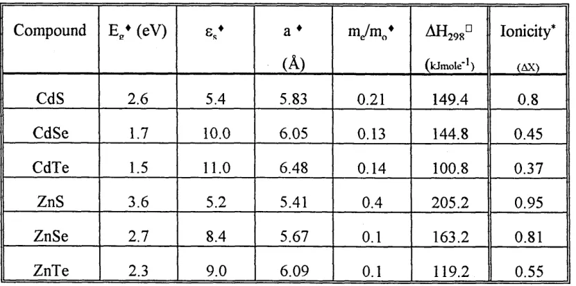
Compound E / (eV) z* a ♦
(A)
a h29*°
(kJm ole'b
Ionicity*
(AX)
CdS 2.6 5.4 5.83 0.21 149.4 0.8
CdSe 1.7 10.0 6.05 0.13 144.8 0.45
CdTe 1.5 11.0 6.48 0.14 100.8 0.37
ZnS 3.6 5.2 5.41 0.4 205.2 0.95
ZnSe 2.7 8.4 5.67 0.1 163.2 0.81
ZnTe 2.3 9.0 6.09 0.1 119.2 0.55
Table 1.1. Physical properties of II-VI compounds. ♦ Ruda (1992). DKubaschewski et al
(1993). ‘following the definition of Kurtin et al (1969).
[image:17.621.79.494.343.549.2]Introduction.
1.2.1 Applications of ZnSe.
The use of ZnSe for optoelectronic applications is evident from table 1.1, with a band gap of 2.7 eV it is an ideal candidate for the production of short wavelength, blue-green light emitting devices and lasers. This property, combined with a close lattice match to GaAs (< 1 %) identifies ZnSe as having excellent potential for incorporation into monolithic blue optoelectronic devices.
Early light emitting devices incorporating ZnSe were produced by Livingstone et al
(1973). n-type ZnSe doped with Al and Mn2+ or Cu2+ to provide luminescent centres was incorporated into a metal-insulator-semiconductor (MIS) structure to produce light in the
^,A u electrode ^
y
Polyimidep* ZnSe — p-ZnSSe ______________________________ ^.p-ZnSe
— CdZnSe quantum well ' n-ZnSe
— n-ZnSSe — n+- ZnSe — n- GaAs buffer
[image:18.618.75.505.316.649.2]— n- GaAs substrate """In electrode
mu uuuuuun.
yellow-orange and blue regions. Gold was used to form a Schottky contact onto a thin layer of ZnO produced by chemical etching of the ZnSe substrate to give electroluminescence in forward bias.
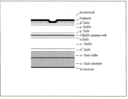
The development of true-blue solid state lasers was severely hindered by the lack of n and
p type doping, a problem which was resolved by Park et al (1990). By doping ZnSe with
nitrogen free radicals generated by a rf plasma source, doping levels of up to lx l0 18cnr3 were readily attained. Using this same technique researchers at 3M in the USA soon
produced the world's first blue solid state laser Haase et al (1990) as depicted in figure
1.2.
Under the application of a forward bias, electrons (n-ZnSe) and holes (p-ZnSe) are injected into the quantum well here they may recombine radiatively to emit a photon. The charge carriers are confined by the ZnSe to the C d^n^S e quantum well The initial photon then interacts with an electron in the conduction band, causing it to recombine with a hole in the valence band stimulating the emission of a second photon. These photons are optically confined by the difference in refractive indices between ZnSe and the ZnSSe cladding region. A Fabry-Perot cavity is produced by cleaving the device at both ends allowing the partial internal reflection required for true laser action. This particular device produced light at the wavelength of 490 nm in the temperature range 77-200K. Since the production of this first device, improvements have been made which allow lasing at room temperature although device lifetimes are still only a matter of a few seconds. The main problems are the high resistance of the metal contact to p-ZnSe Band gap engineering has been suggested as one possible solution and some progress has been made
using graded BeTe/ZnSe and ZnTexSej.x structures by Mensz (1994) and Fan et al (1993)
respectively. A second major problem is the lattice mismatch between ZnSe and the C d ^n ^S e quantum well structure which, upon heating induces dislocations which
UUUl/UUU.
destroy laser action, Guha et al (1993). One solution to this problem has been
demonstrated by Gaines et al( 1993) using Zn1.xMgxSySe1.y as the quantum well structure.
A full review of recent advances made in this very active area of research are given by
Neumark et al (1994) and Prior (1994).
1.2.2 Applications of CdTe and CdS.
A number of parameters make CdTe an ideal candidate for high efficiency low cost photovoltaic solar cells for terrestrial energy conversion. A near ideal band gap of 1.45 eV coincides directly with the maximum power region of the solar spectrum. The short absorption length of photogenerated carriers means that most carriers can be generated within or close to the depletion region, leading to high efficiencies for thin film material. There are many relatively inexpensive methods of producing large area polycrystalline thin films of photovoltaic quality, reviewed by Ullal (1992). CdTe is commonly combined with a wider band gap window material such as CdS which enables the cell to convert a greater proportion of the solar spectrum. Using this configuration high conversion efficiencies approaching a predicted 18% have been achieved, Ullal (1992). Many problems still exist with this technology before it meets the stated goals of the USA Department of Energy of 15% efficiency modules with a 30 year life span, (Annan (1993)). The current state of the art in CdS/CdTe based photovoltaics was reviewed by Chu and Chu (1995) where the reproducibility and instability of metal contacts to these materials was identified as a key area for device improvement.
There are primarily two types of cell in the thin film category. The metal-semiconductor cell in which the active junction is at the interface between the metal and semiconductor and the heterojunction cell in which the active junction is the p-n junction between the two semiconductors. The energy band diagrams of both types of cell are shown in figure 1.3.
>4
(a) Heterojunction (b) Schottky barrier
Figure 1.3 (a) Heterojunction photovoltaic solar cell (b) Schottky diode type photovoltaic solar cell.
The Schottky barrier solar cell requires a semi-transparent metal layer onto n-type material as the front contact. Photons then enter the device via this thin metal layer; photons of energy hu > (j)b are absorbed by the metal forcing electrons over the Schottky barrier, photons with hu >= e 8 enter the semiconductor and create electron hole pairs in the vicinity of the depletion region, the remaining photons with hu « Eg can then create electron hole pairs in the neutral region. Efficiencies of this type of cell were reported by
Fulop et al{ 1982) of « 8.6%. Controlling the magnitude of the Schottky barrier by pre
contact formation treatments such as annealing in air or inert atmosphere can produce a thin oxide layer. This leads to the formation of a MIS structure upon the subsequent formation of metal contacts. Electrons entering the cell tunnel through this insulator and
[image:21.615.63.499.29.355.2]1 1 1 U U U U V U U 1 1 .
pass over the barrier as in the metal-semiconductor device. For thicknesses of insulator of only a few monolayers this can actually increase the efficiency due to an increase in the open circuit voltage. In this manner Raychaudhuri(1987) has reported Schottky barrier MIS cells of «15% efficiency.
A second type of solar cell which has received much attention recently is the heterojunction cell. This normally consists of two materials one of which is doped n-type and the other p-type. The advantage in having a second material is that the larger band gap allows the cell to capture a greater portion of the solar spectrum improving the efficiency of the cell. A schematic of the heterojunction cell together with a band diagram is shown in figure 1.3(a). In this case the window material is formed from n-type CdS which has a band gap of 2.42 eV at room temperature. For the two materials CdTe (Eg =1.45 eV) has the smaller bandgap, CdS therefore forms the window material on the illuminated side of
the cell. CdS is then able to absorb photons with greater hv and therefore shorter X, the
longer wavelengths then go on to be absorbed by the CdTe layer. This produces a cell with a greater spectral response than the Schottky type device and should therefore have a greater efficiency. Of course the thickness of the window layer is vital as there is a compromise between absorption of light and scattering of photons in the CdS. The ideal situation is for the second semiconductor, in this case CdTe, to have a high collection efficiency. In that way the electron-hole pairs are generated close to the depletion region of the p-n junction and efficiency is high. This type of photovoltaic device now accounts for most of the research effort on CdTe solar cells and is the state of the art in thin film photovoltaics. The highest efficiency reported to date was produced by Britt and Ferekides (1993) who claimed an efficiency of 15.8%.
1.3 Aims and objectives.
Most theories of Schottky barrier formation have evolved through experimental observations of elemental or group III-V semiconductors. One of the broad aims of the project was to objectively test the applicability of these theories to metal II-VI compound interfaces. Although much progress has been made previously the level of II-VI compound related knowledge falls far short of that for elemental and III-V compounds. The very nature of metal-semiconductor interfaces is such that any information on the mechanisms of Schottky barrier formation should ultimately lead to a better understanding of the material itself. As well as providing new experimental evidence on metal/II-VI systems regarding the physical models of Schottky barrier formation, the practical insights gained from these studies should lead to new methodologies of contact formation and processing. Ultimately such advances should yield new contact technologies and devices. The scope of the project therefore fell into three broad categories:
• The study of treatments using modem surface analytical techniques which influence the chemical nature and composition of the semiconductor surface. The aim being to establish repeatable processes which can provide a variety of substrates for subsequent metal contact formation.
• The macroscopic electrical properties of metal junctions formed on these surfaces. Having achieved a method of producing different surfaces, metal contacts formed to these surfaces inevitably exhibit different interface properties. The interfacial properties of different metal-semiconductor contacts then relate to the macroscopic behaviour of the contact as a whole.
• The effects of time on such metal contacts in terms of the stability of the devices. Time effects generally introduce a non-abruptness to the interface, or at the very least allow
lllll UUUIH1U11.
a period of time over which chemical reactions can take place between the metal and the semiconductor.
1.4 Approach.
In order to achieve the aims stated above there has from the beginning of the project been a conscious effort to employ methods of semiconductor surface modification which are directly applicable to device manufacture. For many thin film devices and certainly for large area devices such as the photovoltaic cell the only practical method of surface modification is that of wet chemical etching. There have been many previous studies of such techniques which will be reviewed in full in Chapter 3. The wet chemical etching of
CdTe has been shown by Dharmadasa et al (1989) to influence the Schottky barrier height
of Au and Sb contacts on n-CdTe. Surface modifications induced by the chemical
treatments were found to influence the deep level defect structure of CdTe, Sobiesierski et
al (1988) which in turn influenced the barrier height. These results are as yet far from
understood but form an excellent point from which to begin the work. Three materials CdTe, CdS and ZnSe were chosen not only for their technological importance but because a pattern of the behaviour of the group of materials as a whole could then be established. In this manner it is then possible to determine patterns of group behaviour which may be easier to interpret compared with isolated data. The program of work has taken the following outline.
• Wet chemical etching procedures were developed from the literature and applied to all three materials. Initially the surface oxidation of the compound was monitored with X- ray photoelectron spectroscopy (XPS). The effects of different alkaline and acidic
etchants on the oxidation state and stoichiometry of the surface was monitored in order to establish suitable etching procedures.
• Metal contacts were then formed onto selected surfaces and characterised by conventional current transport mechanisms. Chemical etchants which gave surfaces of reduced oxide content were especially investigated, the Schottky barrier characteristics of contacts formed to these surfaces were then monitored.
• Electrical characteristics of these aged metal contacts were monitored macroscopically by I-V techniques; In such a way it was possible to relate microscopic interfacial interactions predicted by the thermodynamics of the interface with the macroscopic device characteristics.
• Intrinsic properties of the semiconductor were analysed by DLTS to determine the possible number of deep levels within a specific material and to investigate the relation of these traps with possible Fermi level pinning at the interface.
• Selected contacts were analysed with state of the art ballistic electron emission spectroscopy (BEES) which allows the Schottky barrier height to be investigated with a spatial resolution in the nm range. Ballistic electron emission microscopy (BEEM) allows the structure of the interface to be related to electronic characteristics. Results from both of these microscopic techniques could then be related to the macroscopic I- V characteristics of specific devices.
— ^ n o u n . v v ij wx k jw ii^invj' u a m c i a .
Chapter 2.
Models and theories of Schottky barriers.
2.1 Introduction.
The Schottky-Mott theory of barrier formation as introduced in chapter 1 is now recognised as a gross over simplification for many metal-semiconductor systems. The mechanism of Schottky barrier formation depends upon a number of parameters including interfacial reactivity, structure, surface/interface states and defects. The main models of Schottky barrier formation described here are all based upon these physical variables.
The function, measurement and physical understanding of the Schottky barrier relies upon the correct interpretation of the current transport and capacitance properties. The main mechanism of current transport, namely thermionic emission over the barrier is discussed collectively with competing processes such as recombination and generation. As it is anticipated that most of the diodes fabricated will have some form of interfacial layer the effects of such layers on current transport and capacitance of the device are also discussed.
2.2 Models of Schottky barrier formation.
Many theories of Schottky barrier formation have emerged, as yet there exists no quantitative predictive theory to explain the magnitude of Schottky barrier height. It is the intention here to provide an overview of the most popular models.
2.2.1. The Bardeen model.
In Bardeen's model of surface states and rectification at the metal-semiconductor interface, (Bardeen (1947)) the first attempt was made to explain the many experimental results which disagreed with the Schottky model. A model was proposed based upon a high density of localised states within the bandgap. It was suggested that if such states were present in sufficient density they would accumulate charge from the semiconductor. An equilibrium level (J)0, (measured from the valance band, Ev) was defined as a level of charge neutrality between filled and empty states at which EF was pinned. The Fermi energies of the bulk semiconductor and the bulk metal must align upon contact between the metal and the semiconductor. If a high density of surface states exist then most of the charge transferred from semiconductor to the metal (and vice versa) will be accommodated by the surface states. The semiconductor is effectively shielded from the charge transfer and the Schottky barrier becomes independent of the metal. EF is effectively pinned by the surface state density. If there is a low density of surface states then charge will be accumulated within the semiconductor which will then follow the
Schottky model.
Bardeen’s model offered an explanation for much anomalous data of the time, (Meyerhof (1947)), but as Bardeen predicted did have a few shortcomings . The main problem was the necessity for an interfacial layer present between the metal and the semiconductor in which to contain the surface states. Heine (1965) was the first to point out that the presence of the metal overlayer modified the surface states and introduced metal-induced gap states within the forbidden band gap.
V
KToO,
•GaS
oo
hCdS f* GaSe
0-6
•ZnSe
o
G^As
InP
[image:28.622.123.408.38.314.2]Electronegativity Difference, AX
Figure 2.1. The "S" curve of interface behaviour after Kurtin etal(1969).
2.2.3. The effective work function model.
The effective work function model of Freeouf and Woodall (1981) assumes that the Schottky model is essentially correct but equation (1.1) should be modified to;
A = 4 # - X, (2.1)
where <|>m, the work function of the metal is modified to 4>eff, an effective work function. The effective work function was assumed to arise as a result of microclusters at the interface, non-stoichiometry, oxide species and metal-semiconductor interaction and is a
--- uoiiiwa.
interface, non-stoichiometry, oxide species and metal-semiconductor interaction and is a weighted average of the work functions of these different phases. It was assumed that (j)eff, would be due in the main part to contributions from the semiconductor anion of work
function through the following reactions;
Anion oxide + Compound >Anion + Cation oxide
M + compound => (Anion or Metal-Anion complex) + M-cation
This type of reaction is often chemically/thermodynamically favourable and so this model has received a lot of attention as it is conceptually very simple. A major problem with quantifying this model is the lack of published data for values of <|)eff for different metal- semiconductor interfaces.
2.2.4 Models of Fermi level pinning.
Following Bardeen's initial predictions of EF pinning, several groups have proposed different mechanisms by which surface/interface states may arise.
2.2.4.1. Metal induced gap states (MIGS) model.
Heine(1965) was the first to predict the existence of states induced within the semiconductor by the metal overlayer rather than the surface states predicted by Bardeen. Heine calculated that the exponentially decaying tails of the metal wave functions would penetrate into the surface of the semiconductor thus introducing states due to the metal
which could then be responsible for "pinning" EF. This work was continued by Flores et al
(1973), the initial motivation being the confirmation of Kurtin's covalent-ionic transition.
i r i v j u v i a a n u U i O U llU U K .y U i l l i l C I S .
They calculated a distribution of states due to A1 and Cu overlayers for a range of zincblende (110) semiconductors. Following the work of Cowley and Sze (1965) where the Schottky barrier height was given by;
h = S f m + b (2.2)
where S was defined as;
5 = ---“~ 7 7 (2.2 (a))
1 + DSe
where, D = density of surface states
5 = effective distance between resonance surface states and opposite charge at the metal surface..
In this manner they were able to construct a curve of S v AX, not to be confused with the "S" parameter adopted by Kurtin. The model was in good agreement for "covalent"
materials but not for "ionic" materials. Tejedor et al (1977) went on to develop this model
further by introducing a level (|)0 at the interface. This neutrality level (|)0, was defined as a level below which all interface charges at the semiconductor surface are cancelled out by the lack of states within the valence band. Again this concept was applied to the Si (111) and the zincblende (110) surfaces. Such a model is not really applicable to strongly ionic crystals such as CdTe, CdS and ZnSe as the electron-electron interaction assumed is by the definition of ionic bonds questionable.
Louis and Flores (1981) applied this model to "real" metal-semiconductor junctions by categorising possible metal-semiconductor interfaces into the following categories;
i T j u u v u u a u m u u i l l / O U 1 J W l U l L K y U t t l i l C I S .
• non-reactive, no chemical compound is formed between metal and semiconductor • etched surfaces, in which the semiconductor has been pre-treated to leave a remnant
oxide layer.
• reactive interfaces, a new chemical compound is formed between the metal and the semiconductor.
From these three categories they drew the conclusions that for clean "covalent" junctions,
the neutral level, §Q was independent of any surface effects and (|)b reached the Bardeen
limit. For "ionic" junctions, Bardeen behaviour can become Schottky-like behaviour with physisorbed layers or the presence of relaxation. With etched covalent surfaces the density of states at <j)0 and hence the ability to pin EF decreases with oxide thickness and hence Schottky - like behaviour ensues.
The MIGS model was again modified by Tersoff (1984) and (1985) in which a branch
point Eb was introduced, calculated from the semiconductor band structure. A low density
of MIGS would draw EF towards EB but would be insufficient to completely remove any dependence upon the semiconductor work function
2.2.4.2 The unified defect model.
In the unified defect model first introduced by Spicer et al (1979) and (1980), EF is pinned
by electronic states due to defects within the semiconductor. Clean surfaces of several III- V compounds (GaAs, InP and GaSb) were studied as sub-monolayer quantities of either metal adatoms or oxygen were added. EF stabilisation was observed at different positions in each material independent of the adatoms being metal or oxygen in origin. In the original model it was assumed that two electronic levels were created due to the removal of anions or cations in the surface region of the semiconductor. Later refinements were
lVAuucia anu mcuiies or acnomcy Darners.
made, Spicer et a/(1986) which proposed that the most likely defects in III-V
semiconductors were of the antisite type where a cation site is occupied by an anion and vice versa. The As on Ga (AsGa) antisite defect was identified as being responsible for deep levels at Ev + 0.74 and Ev + 0.5 eV for GaAs in the advanced unified defect model
Spicer etal (1988).
One crucial difference between the MIGS model and the defect model is that the MIGS model requires the deposition of several monolayers of metal before the metal can assume a true metallic character and band structure to subsequently produce metal-induced gap states. The defect model requires only sub-monolayers of adatoms to induce specific defects. The main analytical treatments of this model have involved specifically III-V compounds, no treatment of II-VI compounds has yet been published.
2.2.4.3. The disorder induced gap states model.
In the disorder induced gap states model of Hasegawa and Ohno (1986), disorder at the surface of the semiconductor induced by the deposition of either a metal or an insulator was found to be responsible for a continum of disorder induced gap states (DIGS). The spectrum of states was said to consist of donor and acceptor - like states with a charge neutrality level between the two, at Eho. EF was then pinned at this level in a similar manner to the MIGS model. For most tetrahedrally bonded semiconductors Hasegawa found the position of EH0 to be largely independent of the specific nature of the disorder. It was calculated that EHO would in fact occur about 5 eV below the vacuum level EVAC, the barrier height would then be given by;
< t > „ = 5 .0 - X s (2.3)
■o u i u u n u L i i v y u a x i i C i S .
Equation 2.3 implies that (j)b, should be largely independent of the metal and the surface preparation procedure used. One advantage of this model over other models of EF pinning is that it allows for pinning in the presence of a thin oxide layer.
2.2.5 The pinch - off model.
Inhomogeneities at the metal semiconductor interface were first proposed by Ohdomari et
al (1979) and Ohdomari and Tu (1980) to be responsible for many anomalies observed in
metal-semiconductor device characterisation by current-voltage (I-V) and capacitance-
voltage (C-V) techniques. Freeouf et al (1982) incorporated a similar model into their
EWF model. Both groups worked on the principle that interfacial inhomogeneities would lead to the formation of a number of diodes under one metal contact. The current transport properties of these devices would then resemble a number of parallel diodes. More recent work by Tung (1991) suggested that previous models of parallel conduction were in serious error when the inhomogenities of the Schottky barrier height were on a scale less than or comparable to the depletion width. No specific mechanism of Schottky barrier inhomogeneity was implied, the Schottky barrier was said to be a ’’function of the interface atomic structure’’. One important consideration that previous models of inhomogeneity had failed to consider was the effect of "pinch-off'. The "pinch-off' effect describes the action of a region of high Schottky barrier height on a small "patch" of lower barrier height, in a similar manner to the operation of a field effect transistor. The conduction path of the lower barrier is "pinched - off' by the barrier of greater magnitude. An area can be described as "pinched- off' if majority carriers originating from outside the space charge region have to traverse a barrier higher than the band edge position at the metal-semiconductor interface, in order to reach the interface. Tung (1992) investigated at
great length the effects of dimensions and area ratios and together with Sullivan et al
(1991) explained many anomalies of normal Schottky barrier measurement. The
.y u a u i c i 5 .
off' model was used to explain such effects as greater than unity ideality factors, temperature dependence of the ideality factor and differences in Schottky barrier height depending upon the measurement technique employed. Tung (1993) has questioned many of the models outlined above particularly models of EF pinining. Agreement between this model and a large body of experimental data was demonstrated although no comparison with data from II-VI compounds has been made.
2.2.9 Summary of models.
It is apparent that there are many models of Schottky barrier formation. Those outlined above are generally considered in the literature to be significant attempts at explaining the physics of the Schottky barrier. Several empirically based models also exist such as the "two-thirds " model of Mead and Spitzer (1964) which have received little attention in the literature from the last decade or so. It seems plausible that more than one of these physical phenomena may exist at the same time, a possibilty which has been proposed by Williams (1991) but which none of the models recognises. Tung's model of Schottky barrier inhomogeneity has been extensively tested against metal contacts to Si and also explains many of the anomalies of normal Schottky barrier theory. No application of this model to II-VI compounds has as yet been made.
2.3 Current transport mechanisms.
The transport of electrons from the semicondcutor to the metal and vice versa is the primary function of all metal contacts, understanding the mechanisms of current transport is therefore fundamental to the operation of the Schottky barrier.
u v.i u ^ u u i i a j ' u a i 11C1 O.
2.3.1 Thermionic emission.
The primary current transport mechanism in Schottky barriers is thermionic emission over the barrier. Contacts in which this is the sole mechanism of current transport are described as ideal.
In Bethe's thermionic emission theory as described by Rhoderick and Williams (1988) the main current limiting phenomena is the emission of electrons over the potential barrier. Drift and diffusion of carriers through the depletion region are assumed to be negligible. Figure 2.2 shows the position of the quasi - Fermi level for electrons which remains flat throughout the semiconductor. For an applied forward bias of V, there is an exponential increase in the concentration of electrons at the semiconductor side of the interface given as a function of Nc, the density of states in the conduction band. The total electron concentration ne, on the semiconductor side of the interface is given b y ;
ne = N c
exp
kT (2.4)
Kinetic theory gives the electron flux incident upon unit area of the interface as n v I A,
where v is equal to the mean thermal velocity of electrons in the semiconductor.
The current density is given by ;
qN v
—>/ exp kT
-
v)']
(2.5)u i o v iiu iirv jr u a i l l U S .
Figure 2.2. The position of the quasi-Fermi level for an applied bias V according to thermionic emission theory after Rhoderick and Williams (1988).
There is a complementary flow of electrons from the metal into the semiconductor, however from the metal side of the interface the application of the bias V has no effect on
the barrier. The metal is effectively presented with a zero bias situation ie V = 0.
The current density from the metal into the semiconductor, Jm^ s, is given by;
q N v
J
=
exP
( -J li.A ^kT j (2.6)
The total net current is then equal to:
J = Jj —rm — J Vm —t s (2.7)
[image:36.620.107.450.26.289.2]ivxuucia auu uicuiics ui ouiiuiiK.y oamers.
qN y
J =
exp
kT J
exp
r qV 's
KkT j (2.8)
For a semiconductor with a Maxwellian distribution of electron velocities, the mean
velocity of electrons is equal to, v = (8kT / 7Dn *) , where m*is the effective mass
of electrons in the semiconductor. The density of states within the conduction band Nc, is given by;
N = 2f l m ' k T Y 2
K. h* j (2.9)
If these substitutions are made into equation (2.8) the total current due to thermionic emission is equal to ;
J = A * T 2 exp
kT exp
qV_
kT - J (2.10)
where,
A* = 4 7Qn *qk 2 / h 3 (2.10(a))
and is equivalent to the Richardson constant for thermionic emission but the free electron mass m is replaced by the effective electron mass m*.
o \jx kjv n v n u i v y u a i i i ^ l d .
Equation (2.10) is often written in the literature as,
j =j . (2.11)
where J0, the saturation current density is,
(2.11(a))
Equation (2.11) is the equation of ideal thermionic emission in the Schottky barrier, assuming that <|)b is independent of applied bias V.
2.3.1.1 Deviations from ideal thermionic emission.
There are many phenomena which cause the current transport to deviate from that described by equation (2.11) above.
2.3.1.2 Image force lowering.
Intimate contacts ie devoid of an interfacial layer, display a bias-dependent reduction in
the barrier height due to the image force as shown in figure 2.3. This reduction in the barrier height Ac^, is related to the Schottky barrier height (J)b, by the following equation,
(2.12)
.ivy u m i i c i s .
E,
FFigure 2.3. The effects of image-force on the conduction and valence bands after Rhoderick and Williams (1988).
If the bias dependence of <j)e is linear (5c|)e/5V is equal to a constant, P) then the effective barrier height can be re-written as;
A = ( A ) . “ ( A d ) , + p v (2.13)
Applying this bias dependence of the Schottky barrier height to the equation for thermionic emission gives;
( qV \ [
(~qV ^
J = J n
exp ——
<
1
- exp —-—
VnkT ){
{ kT
(2.14)ivioaeis ana tneones or bcnottky barriers.
The ideality factor, n, is usually introduced at this stage, the main function of which is to define the quality of the diode. It is in fact a literal expression of the bias dependence of the Schottky barrier height, in this case is written as,
L = 1 P = 1 ^
-n S v (2.15)
Typical values for II-VI materials doped in this range give n « 1.02 which can be considered as the theortical limit of the ideal Schottky barrier. The saturation current J0 is now modified to be;
J 0 = A T 2 exp
'((A).-(A*,).)'
kT (2.16)
2.3.1.3 Recombination and generation.
A common mechanism of current transport is the recombination of electron hole pairs via recombination centres within the band gap. Recombinaion centres may be intrinsic to the material or extrinsically introduced by surface imperfections or interfacial defects. Those centres which occur close to the centre of the band gap were proposed as the most efficient recombination centres in the model developed by Shockley and Read (1952). The recombination current density at low forward bias is given by,
ivxuucis emu uicuncs ui acnuiiKy Darners.
(2.17)
where
(2.17(a)
rij is the intrinsic electron concentration, w is depletion region thickness and Tr is the
are several shortcomings to this theory namely;
• the energy levels of the recombination centres coincides with the intrinsic level. • the capture cross-sections for electrons and holes are equal.
• the recombination centres are distributed uniformly.
Equation 2.17 can therefore be considered as a simplification of the real situation.
The total current density, JTot, from a combination of the thermionic and recombination currents is given by;
carrier lifetime within the depletion region. Rhoderick and Williams point out that there
J T = J + JTot te r (2.18)
JTot (2.18(a))
aim intvjiics ui ouuvjuis.y uamcis.
T 2 Tr exp <{ qa“ ---(e, + V -2<l>b)O 7,'T
2kT (2.19)
From the above relation it is evident that recombination current is more prevalent in semiconductors with high Schottky barriers, in material with a low carrier lifetime and at low applied forward bias. The ratio of thermionic emission to recombination also increases with temperature so recombination will therefore be more noticeable at low temperatures for a particular diode.
2.3.1.4 Quantum mechanical tunnelling.
Quantum mechanical tunnelling may occur in two possible modes dependent upon the temperature, T and donor concentration Nd. Field emission occurs most noticeably in heavily doped semiconductors at energies close to EF. As the temperature increases electrons are given more energy and so can pass through the barrier at a higher energy than Ef, this process is known as thermionic field emission. At even higher temperatures the dominant process is thermionic emission.
Padovani and Stratton (1966) formulated an exact treatment of quantum mechanical tunnelling which was reviewed by Rhoderick and Williams (1988). The parameter E00 was defined such as;
Eo o (2.20)
iviuucis anu tneunes 01 acnoiiKy Darners.
and determines the probability of an electron tunnelling. £s is the semiconductor
permittivity (£r x £*0), m * is the effective mass of electrons in the semiconductor
(m r x me). E00 for CdTe, CdS and ZnSe, assuming a doping concentration of «5 x 10²²
nr3 (5 x 1016 cm-3) was calculated to be 3.35, 3.9 and 3.83 meV respectively which is approximately equal to 1/lOkT at T = 300K (= 25.8 meV). This shows that thermionic emission will be the dominant process in contacts to these materials at these donor concentrations.
2.3.1.5 Interfacial layers.
The current transport properties can be influenced a great deal by the presence of thin interfacial layers which are almost inevitable in most practical devices not prepared under UHV conditions. Figure 2.4 shows a schematic idealised energy band diagram of a metal- insulator semiconductor (MIS) Schottky barrier. Typically, interfacial layers are formed from oxide films although they may be too thin to develop the full band structure of an insulator. The analysis of Card and Rhoderick (1971) assumes a thin insulating layer of thickness 8. On the application of a forward bias V, some of the potential is dropped across the interlayer introducing a bias dependence of the Schottky barrier height. The presence of the insulating layer means that thermionic current is reduced by the finite probability of electrons then tunnelling through the layer, the thicker the layer then the less is the current. The modification of the current voltage relationship can be understood by a modification in the diode quality factor, n. A relationship for the diode quality factor was derived by Card and Rhoderick (1971), where;
iviuucis anu meones or acnottKy oamers.
6
i 1
Zero bias - - Forward bias, V
Figure 2.4 A Schottky barrier with an interfacial layer.
{8 1 £,) {{ ss I w) +qD Ib]
n = 1 + ---j ---- r--- (2.21)
1 S,)
In this analysis the interface states are divided into two groups of densities Dsa and Dsb. The first group Dsa, can be considered to be in equilibrium with the metal and thus hold (j)b constant, the second Dsb are in equilibrium with the semiconductor and hold Vd constant, increasing n. Rhoderick and Williams state that a thin film of Si02 in which 5 < 30 A thick would produce n « 1.3-1.5. These values are however dependent upon es and 8j of the particular semiconductor and oxide or interfacial film.
iviuucis anu meones or acnottKy Darners.
2.4 Capacitance of a Schottky barrier.
The depletion region of the Schottky barrier can in many respects be considered as a voltage dependent capacitor. In the ideal case where minority carriers are negligible, the effect of holes can be neglected providing the barrier height is in excess of 3kT/q. For an applied reverse voltage Vp the induced band bending will be equal to the diffusion voltage Vd. Following the exact analysis of an electric field in a Schottky barrier of Rhoderick and Williams, the maximum electric field due to uncompensated donors is given by;
E
2
max_ 2qN
(2.22)
Gauss's theorem states that charge due to uncompensated donors is given by the expression;
q^ a , = ssEmax (2.23)
= ( 2 q e , N d )1 / 2 r v - kJ L
v * q
1 / 2
(2.24)
The capacitance of unit area is defined as ;
dQd dQd
c = j l r = ^ r (Z 2 5 )
differentiating equation 2.24 with respect to Vd gives ;
iviuuvio emu mtuiica ui ociiuuK.y Darners.
c =
112/V 2 j V
vd
-kT - l / 2
(2.26)
The band bending, Vd induced by an applied reverse bias Vr is equal to Vd = Vr + Vd0.
where Vd0 is the band bending at zero bias and in turn is equal to Vd0 = <j)b - \ is the
difference between EF and the bottom of the conduction band, Ec. If these expressions for Vd are substituted into equation 2.26 the capacitance of the Schottky barrier due to a reverse bias Vn becomes;
C = q e, N <
1 / 2
A - £ + v . kT
<1 J
(2.27)The capacitance of the Schottky barrier is normally measured using a small a.c. carrier signal superimposed upon a d.c. bias signal as explained in Sec 4.4.2.
2.4.1. Deviations from the ideal capacitance.
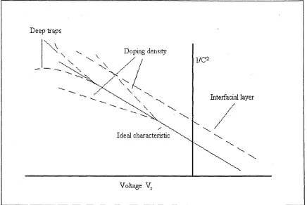
As with electron transport over the barrier there are several mechanisms which commonly occur in real devices which have a profound influence on the capacitance of the Schottky barrier. These are namely interfacial layers between the metal and semiconductor and deep traps within the band gap.
2.4.1.1 Interfacial layer effects.
The effects of thin interfacial layers on the capacitance of the Schottky barrier have been discussed in detail by Cowley (1966) and Crowell and Rideout (1969). The band diagram
iviuucis anu meunes or acnottKy Darners.
of such a layer will of course look much the same as that of figure 2.4. If the interfacial layer is sufficiently thin then the occupancy of interface states is governed predominantly by electrons tunnelling from the metal. In Cowley's analysis the plot of C 2 versus Vr
remains linear with gradient of 2 / q£s N d but the intercept on the Vr axis is increased
from Vj to Vj.given by;
The parameter a accounts for the increase in the intercept and is largely dependent upon the thickness of the interfacial layer, 5, the permittivity of the interfacial layer ei5 and the density of states of the layer Ds.
2.4.1.2. Deep traps.
Deep traps can be considered as localised electron states within the bulk of the semiconductor. The term "deep" implies they are energetically far from either the valence or conduction band and are therefore not ionised at room temperature. The occupation of the trap varies in the depletion region of the Schottky barrier as shown in figure 2.5. Those traps below EF are occupied by electrons, those above are empty and have a net positive charge. The state of occupation and therefore the state of charge will depend upon the degree of band bending which in turn is dependent upon the bias voltage applied to the device.
q ; 28, (2.27)
where;
(2.28) £. + q§D
u n u 1^0 u i o ^ m j l l t y y U c l l l l C l S .
The degree of influence of deep traps on the overall charge in the depletion region and hence the capacitance is largely dependent upon the test frequency employed. It is normal to make capacitance measurements with an a.c. bridge operating with a d.c. bias and a sinusoidal a.c. test signal of frequency cos The rate of change of the d.c. signal is much less than the a.c. test signal and so can be ignored. The contribution the traps have to the overall capacitance will depend upon the speed at which the traps open, fill and empty. The influence of the traps is therefore a function of the ratio of cos to x^1 ( = 2en )_1 where en is the probability of a trap emitting an electron into the conduction band in unit time .
E,
FFigure 2.5 Charge state of deep traps under zero bias.
Keview ot literature.
Chapter 3
Review of literature._______________________________
3.1 Introduction.
The study of metal - semiconductor contacts can be divided into three broad areas, namely semiconductor surface studies, current transport across the metal - semiconductor interface and deep levels within the semiconductor. A thorough understanding of the physics and chemistry of the metal - semiconductor interface can not be gained without considering these physical properties for the systems under investigation. Presented here is a review of the key works in these three areas for CdTe, CdS and ZnSe. It is apparent from the literature that interest in these various topics is driven by the applications of the materials. For instance, early studies of CdTe surfaces concentrated on wet chemical etching in an attempt to control electrical properties whereas now many papers are concerned with etchants for producing substrates suitable for epitaxial growth of CdTe and lattice matched compounds.
3.2 Experimental surface studies of CdTe, CdS and ZnSe.
The literature contains much information on the surface analysis of CdTe and CdS but very little on ZnSe. The main issues discussed are the characterisation of native oxides and modifications induced by wet or dry etching and annealing.
3.2.1 Surface studies of CdTe.
Keview or literature.
Ambiguities remain in assigning the correct native oxide chemical composition and etching mechanisms. Problems arise due in part to the various chemical shifts associated with either Te-0 bonds or Cd-0 bonds. Perhaps the more obvious oxidation state is that of Te02 which produces a chemical shift of some * 3.4 eV from the Te 3d5/2 peak (Briggs and Seah(1990)). The various native oxides of Te all produce noticeable shifts in the Te 3d peaks. The Cd 3d peaks pose a different problem in that any shift they produce is typically much less than 1 eV and is therefore difficult to detect with conventional spectrometers. Cd 3d5/2 peaks associated with Cd-Te bonds have binding energies of 405.2 eV whereas those of the native oxides such as CdO and CdTe03 are 404.2 eV and 405.5 eV respectively (Briggs and Seah (1990)). Further information regarding the chemical state of Cd can be obtained through analysis of the X-ray generated Auger electron features. Al and Mg X-ray sources generate strong Auger spectra associated with transitions in the Cd MNN shell. The Auger features associated with the Cd M4N45N45 and M5N45N45 transitions show energies and shapes which are markedly different if the Cd atoms from which they originate are bonded Cd-Te or Cd-O. In this manner a qualitative analysis of the level of Cd oxidation can be determined. Care must be exercised when employing this type of analysis as, with Mg Ka radiation the Cd M4N45N45 peak actually overlaps with the Te 3p1/2 photoelectron peak. The confusion in correctly assigning the native oxides of CdTe may explain why there seems to be some disagreement within the literature as to the composition of the native oxide. One school of thought suggests that the native oxide can be accounted for purely by the oxidation of Te whereas a second group cites contributions from Cd and Te to the total oxidation of the surface. It should be noted that of the groups proposing Te oxidation, most have not monitored the Cd Auger features for any evidence of Cd oxidation.