N A N O E X P R E S S
Open Access
Structural, electrical, and optical properties of
Ti-doped ZnO films fabricated by atomic layer
deposition
Zhi-Yuan Ye, Hong-Liang Lu
*, Yang Geng, Yu-Zhu Gu, Zhang-Yi Xie, Yuan Zhang, Qing-Qing Sun, Shi-Jin Ding
and David Wei Zhang
Abstract
High-quality Ti-doped ZnO films were grown on Si, thermally grown SiO2, and quartz substrates by atomic layer deposition (ALD) at 200°C with various Ti doping concentrations. Titanium isopropoxide, diethyl zinc, and deionized water were sources for Ti, Zn, and O, respectively. The Ti doping was then achieved by growing ZnO and TiO2 alternately. A hampered growth mode of ZnO on TiO2layer was confirmed by comparing the thicknesses measured by spectroscopic ellipsometry with the expected. It was also found that the locations of the (100) diffraction peaks shift towards lower diffraction angles as Ti concentration increased. For all samples, optical transmittance over 80% was obtained in the visible region. The sample with ALD cycle ratio of ZnO/TiO2being 20 had the lowest resistivity of 8.874 × 10⁻⁴Ωcm. In addition, carrier concentration of the prepared films underwent an evident increase and then decreased with the increase of Ti doping concentration.
Keywords:TZO films, ALD growth rates, Structure characteristics, Optical properties, Electrical properties
Background
The application of transparent conductive oxide (TCO) has been found in many areas such as liquid crystal dis-plays, touch panels, and organic light-emitting diodes because of its excellent conductivity and high transmit-tance for visible light [1-4]. At the moment, indium tin oxide film is the most popular material and has been widely used in many optoelectronic devices. Although it has excellent transparency (greater than 85% transpa-rency in visible spectrum) together with high conducti-vity (resisticonducti-vity around 2 to 4 × 10⁻⁴Ω cm) [5], research on alternative materials is urgent due to the relative scarcity and high cost of indium.
Several alternative TCO materials have been investi-gated extensively recently. Among them, ZnO seems to be one of the ideal choices due to its low cost. As is well known, ZnO is a II-VI group semiconductor material containing high concentration of native defects, which typically include oxygen vacancies or zinc interstitials. Thus, pure ZnO has excellent conductivity. However,
pure ZnO thin films are not very electrically and che-mically stable at high temperature [6]. Fortunately, the performance of ZnO thin films can be improved by ap-propriate impurity doping [7]. For example, it has been reported that Al-doped ZnO film fabricated by atomic layer deposition (ALD) has as high as 80% to 92% trans-mittance in the visible range and low resistivity around 4 × 10⁻³Ω cm [8]. What is more, as is reported by Lin et al., Zr-doped ZnO thin films grown by atomic layer deposition with sapphire substrates have wonderful transparency (>92%) for visible light and high carrier concentration (2.2 × 10²⁰) [9].
Among the variety of metallic element-doped ZnO films, Ti-doped ZnO films have been investigated re-cently for their unique electrical, magnetic, and sensing properties. In some previous studies, a number of fabri-cation techniques such as sputtering, pulsed laser depo-sition, and chemical vapor deposition (CVD) as well as the structural, morphological, and electrical characteris-tics of the corresponding films [10-16] have been discussed. However, rare reports focused on Ti-doped ZnO films fabricated by ALD. Furthermore, compared with those of main group metal-doped ZnO films, the
* Correspondence:[email protected]
State Key Laboratory of ASIC and System, Department of Microelectronics, Fudan University, Shanghai 200433, China
conduction mechanisms of ZnO films doped with transi-tion metals such as Ti are still not clearly understood. So it is of greater importance to do research on Ti-doped ZnO (TZO) films grown by ALD. In this work, the effect of Ti doping concentration on the structural, optical, and electrical properties of the deposited TZO
films was systematically studied by spectroscopic
ellipsometry, X-ray diffraction, atomic force microscopy, transmission spectrometry, and Hall measurement.
Methods
TZO thin films were deposited at 200°C in a BENEQ TFS-200 ALD reactor (Vantaa, Finland) using titanium tetraisopropoxide liquid (TTIP), diethyl zinc (DEZ), and deionized (DI) water. TTIP, DEZ, and DI water were used as Ti, Zn, and O sources, respectively. The precur-sors TTIP and DEZ were separately held in stainless bubblers at 58°C and 18°C, respectively. High-purity quartz, thermally grown SiO2, and silicon served as the
substrates. Before loading into the ALD reactor, the quartz glasses were ultrasonically cleaned with acetone and alcohol in sequence for 5 min, and then rinsed with DI water and dried in nitrogen. The silicon substrates were cleaned chemically using a standard Radio Corpo-ration of America solution (New York, NY, USA) and then dipping into the diluted 5% HF solution for 1 min to remove the native oxide layer, followed by rinsing with DI water and drying in N2. The precursors were
al-ternately introduced to the reactor chamber using high-purity N2 (>99.99%) as the carrier gas. A typical ALD
growth cycle for ZnO is 0.5-s DEZ pulse/2-s N2 purge/
0.5-s H2O pulse/2-s N2 purge, whereas for TiO2, it is
1.0-s TTIP pulse/5-s N2 purge/0.5-s H2O pulse/5-s N2
purge. The TZO films were then achieved in an ALD supercycle mode, which was defined as N ZnO cycles followed by one TiO2 cycle. Supercycles were repeated
until the target number of 500 ZnO cycles was reached. The thicknesses of TZO films were measured by spec-troscopic ellipsometry (GES5E, SOPRA, Courbevoie, France) wherein the incident angle was fixed at 75° and the wavelength region from 230 to 900 nm was scanned with 5-nm steps. The crystal structures of films were obtained using an X-ray diffractometer (D8 ADVANCE, Bruker AXS, Madison, WI, USA) using Cu Kαradiation (40 kV, 40 mA,λ= 1.54056 Å). Atomic force microscopy (AFM) using a Veeco Dimension 3100 scanning probe microscope (Plainview, NY, USA) operated in a tapping mode provided surface morphology of the TZO thin films. To obtain the optical transmission spectra, a UV spectrophotometer (UV-3100) in a wavelength range of 200 to 900 nm at room temperature was used in the air. In addition, the electrical properties of TZO films depo-sited on thermally grown SiO2are characterized by Hall
effect measurements using the van der Pauw method.
Results and discussion
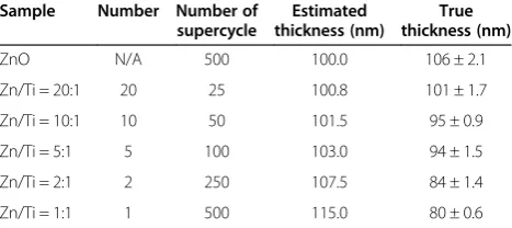
The growth per cycle (GPC) of pure ZnO and TiO2
films are tested to be 0.2 and 0.025 nm/cycle, respect-ively. Measured thicknesses of TZO films are then listed in Table 1 together with the expected thicknesses, which are given by
Thickness¼500GPCZnOþ500N GPCTiO2; ð1Þ
In Equation 1, it is assumed that the GPC for a given material has no business with the material deposited in the previous cycle. Since the GPC of ZnO is much greater than that of TiO2, the estimation of the film
thickness is accurate provided that ZnO encounters no barrier to grow on TiO2. As an example, for the TZO
film with N= 20, the measured thickness is 101 nm, which is very close to the expected one. However, with further increase of Ti doping concentration, the mea-sured film thicknesses are found to be off-target.
Espe-cially, in the case of the sample with N= 1, the
measured thickness was found to be around 80 nm, which was much smaller than the ideal one (115.0 nm). Thus, it is inappropriate for us to assume the GPC of ZnO on TiO2 to be 0.2 nm/cycle. The black squares in
Figure 1 show the true thickness as a function ofN. To model the true growth process of ALD-ZnO film on TiO2 layer, a method similar to that reported by
Banerjee et al. [8] was employed. The decrease of the GPC of ZnO may result from the reduced adsorption of DEZ on TiO2. Thus, it is appropriate to assume that the
GPC of ZnO follows an exponential behavior given by
GPC0
ZnO¼A 1eni
; ð2Þ
whereGPC0ZnOrepresents the GPC of ZnO in TZO film, Ais the GPC of pure ZnO film, the independent variable i is the ith cycle number after TiO2deposition, and the
parameter n refers to the number of cycles it needs for GPC0
[image:2.595.305.539.628.732.2]ZnOto reach 63.2% of the ideal growth rate of ZnO. According to Equation 2, theGPC0ZnOwould be close to that observed in pure ZnO films after enough number of
Table 1 Summary of estimated and measured thicknesses
of TZO films withR2accuracy greater than 0.995
Sample Number Number of
supercycle
Estimated thickness (nm)
True thickness (nm)
ZnO N/A 500 100.0 106 ± 2.1
Zn/Ti = 20:1 20 25 100.8 101 ± 1.7
Zn/Ti = 10:1 10 50 101.5 95 ± 0.9
Zn/Ti = 5:1 5 100 103.0 94 ± 1.5
Zn/Ti = 2:1 2 250 107.5 84 ± 1.4
ZnO cycles. It is also appropriate to assume that GPC0
TiO2 remains unchanged throughout the whole
process since TiO2is always deposited on ZnO.
Consid-ering all the assumptions above, the total thickness of the film can be given by
T¼ XNi¼1GPC0ZnO 1eni
þt
h i
500N ; ð3Þ
whereTdenotes the total thickness and the constanttis the GPC of TiO2. Using this function model to fit the
measured data, the parameter ncan be calculated to be approximately 1 whiletis approximately 0.024 nm/cycle. Thus, it can be concluded that TiO2 encounters little
barrier to grow on ZnO.
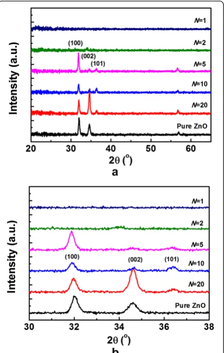
Figure 2 shows the XRD patterns of as-deposited TZO films on quartz. As is displayed in Figure 2a, the crystal-linity of the films depends on the N. No phases related to TiO2or Zn2TiO4are detected in the scanning range.
Usually, the [002] direction, i.e., thec-axis, is the prefer-ential orientation commonly occurring in pure ZnO films and doped ZnO films prepared by other fabrication techniques such as sol–gel, CVD, and sputtering [10]. However, in the current samples, the (100) peak grad-ually becomes dominant and the (002) peak turns to be weaker as Ti doping concentration increases. The (100)
peak reaches a maximum for the sample with N= 5.
However, no peak can be observed in the samples with
N= 2 and 1, indicating that the TZO films become
amorphous with too much Ti doping. It is well known that the (002) plane of ZnO consists of alternate planes of Zn2+and O2−and thus is charged positively or nega-tively, depending on surface termination. On the other hand, the (100) plane is a charge neutral surface consisting of alternate rows of Zn2+and O2−ions on the surface. Thus, it is conceivable that the layer-by-layer growth during ALD may cause the Ti4+ ions to disturb
the charge neutrality of the (100) plane, thereby affecting its surface energy and causing its preferential growth [8]. In addition, the locations of the (100) diffraction peaks shift towards lower diffraction angles as Ti concentration increases, as shown in Figure 2b. To understand this phenomenon, it is worthwhile to notice that the valence of Ti tends to be +4 in the TZO films made by atomic layer deposition. Along the [100] direction, the film layer is composed of the line of Zn2+ ions or the line of O2−. If Ti4+ ions take the place of Zn2+ sites, the repulsive force in this direction would increase because of extra positive charge. This effect can enlarge the interplanar spacing along the [100] direction, thus leading to the ob-served decrease of the diffraction angle.
[image:3.595.307.539.89.453.2]The AFM images of the films deposited on silicon sub-strate were measured to further characterize the effect of Ti doping concentration on the surface morphology of TZO films. Figure 3 shows the AFM images of these films and their root mean square (rms) surface rough-ness in a scan size of 2 × 2 μm2. It was found that the
Figure 1Fitting curve according to the function model is shown with a red solid line.
[image:3.595.58.295.89.256.2]rms roughness value of the films except for the sample with N= 1 is in the range of 1.65 to 1.80 nm. The sur-faces of these films are evidently smoother than those deposited by RF reactive magnetron sputtering [10]. It highlights the potential use of TZO films made by ALD as TCO, where precise control over film uniformity and smoothness is required. The film with N= 1 shows the
[image:4.595.56.291.488.707.2]Figure 3AFM images of TZO films with rms surface roughness in a scan area of 2 × 2μm2.
Figure 4Transmission spectra of TZO films with various Ti concentrations.The inset shows the plot of (αhv)2versus
hv.
[image:4.595.305.539.570.705.2]lowest surface roughness with its rms roughness value to be 0.59 nm. In addition, no etching effect on the film is found in the experiment [17].
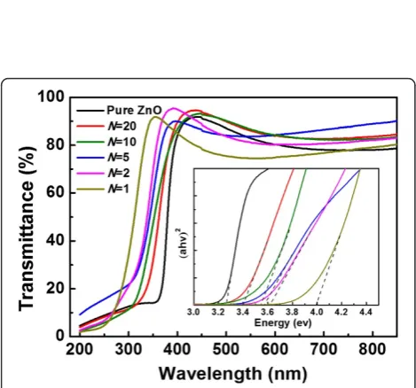
Figure 4 displays the transmission spectra of TZO films grown on quartz. It is obvious that an average op-tical transmittance more than 80% in the visible range is obtained for the samples with Nfrom 20 to 2, which is valuable for TCO applications such as liquid crystal dis-plays. The relatively low transmission for the sample grown with N= 1 resulted from the high concentration of Ti in the TZO films. Moreover, all the films show a sharp absorption edge in the ultraviolet range, which shifts to the lower wavelength side with Ti concentration increase. The optical band gap of TZO thin films can be calculated according to the transmission spectra. As a direct-band gap material [18], it is reasonable to assume that the absorption coefficient (α) is proportional to− ln(T), where Tis the optical transmission. According to the Tauc relationship, the relation between the optical band gap (Eg) and absorption coefficient is given by [19]
αhv∼hvEg1=2; ð4Þ
where h is Planck's constant and v is the frequency of the incident photon. The Eg of the TZO films can be
obtained by drawing the plot of (α×hv)2versus the pho-ton energy (hv) and extrapolating a straight line portion of this plot to the axis of photon energy, as is indicated in the inset of Figure 4. It can be found that the band gap energy increases from 3.26 eV for pure ZnO film to 3.99 eV for the film with N= 1. The widening of band gaps with the increase of titanium concentration is ge-nerally attributed to the Burstein-Moss band-filling ef-fect. Excessive carriers induced by the doped Ti would fill the conduction band edge, so the optical band gap is widened [20,21].
To investigate the electrical properties of the TZO thin films, Hall measurements are carried out at room temperature. The thermally grown SiO2 was chosen as
the substrate since the substrate needs to be insulative. The dependence of carrier density, resistivity, and mobi-lity on Ti contents in the TZO films is shown in Figure 5. It should be noted that the resistivity of the sample with N= 1 is so large that its mobility and carrier concentra-tion cannot be measured accurately. As is displayed, the resistivity, mobility, and carrier concentration for pure ZnO films prepared by ALD are 2.14 × 10⁻³Ωcm, 1.4 × 1020 cm−3, and 22.5 cm2/V · s, respectively. The resisti-vity of the TZO film withN= 20 at first drops to a mini-mum value of 8.874 × 10⁻⁴Ωcm and then goes up with the increase of the Ti contents. It suggests that the con-ductivity of ZnO film can be improved significantly with appropriate Ti doping concentration. On the other hand, the maximum carrier concentration of 6.2 × 1020cm−3is
achieved for the sample with N= 10, which is higher than that reported by Park and Kim [22]. However, car-rier concentration of the TZO film undergoes an abrupt drop when more Ti impurities are introduced into the TZO film. The decrease in the carrier concentration can be interpreted as follows: As the Ti doping concentra-tion continues to increase, some titanium atoms tend to aggregate near grain boundaries to form TiO2instead of
taking the place of Zn2+ to generate more free carriers [23]. The widening of band gap is also generally consid-ered as a dominant mechanism contributing to the de-crease of carrier concentration [20,21]. In addition, the mobility of TZO films decreases from 21.7 cm2/s for pure ZnO to 2.3 cm2/s for the sample with N= 2. The decrease in mobility is apparently due to the increase of carrier scattering, the deterioration in the crystalline quality, and formation of TiO2at the grain boundaries.
Conclusions
Ti-doped ZnO thin films with the thickness of around 100 nm were prepared by ALD at 200°C. The fact that film thicknesses measured by spectroscopic ellipsometry were thinner than expected for samples with ALD cycle ratio of ZnO/TiO2 less than 10 suggested a hampered
growth mode of ZnO on TiO2 layer. TZO films
synthetized by ALD crystallized preferentially along the [100] direction. High transparency (>80%) in the visible region was obtained, and the band gap of the TZO films increased with increasing Ti doping concentration due to the Burstein-Moss effect. It was observed that the resistivity of TZO film had a minimum value of 8.874 × 10⁻⁴Ωcm when the ALD cycle ratio between ZnO and TiO2was 20.
Competing interests
The authors declare that they have no competing interests.
Authors’contributions
The experiment was designed by ZYY and HLL and revised by QQS, SJD, and DWZ. The fabrication of TZO films was carried by ZYY and YG. The characteristics of the films were tested and analyzed by ZYY with the help from YG, YZG, ZYX, and YZ. ZYY prepared the manuscript, and HLL gave a lot of help with the draft editing. All of the authors have read and approved the final manuscript.
Acknowledgments
This work is supported by the Important National Science & Technology Specific Projects (2011ZX02702-002), the National Natural Science Foundation of China (no. 51102048), SRFDP (no. 20110071120017), and the Independent Innovation Foundation of Fudan University, Shanghai.
Received: 18 November 2012 Accepted: 31 January 2013 Published: 27 February 2013
References
1. Lewis BG, Paine DC:Applications and processing of transparent conducting oxides.MRS Bull2000,25:2.
2. Shah A, Torres P, Tscharner R, Wyrsch N, Keppner H:Photovoltaic technology: the case for thin-film solar cell.Science1999,285:692. 3. Jagadish C, Pearton S:Zinc Oxide Bulk, Thin Films and Nanostructures.Oxford:
4. Shan FK, Liu GX, Lee WJ, Shin BC:The role of oxygen vacancies in epitaxial-deposited ZnO thin films.J Appl Phys2007,101:053106. 5. Kim H, Gilmore CM, Pique A, Horwitz JS, Mattoussi H, Murata H, Kafafi ZH,
Chrisey DB:Electrical, optical, and structure properties of indium-tin-oxide thin films for organic light-emitting devices.J Appl Phys1999,6451:86. 6. Singh AV, Mehra RM, Buthrath N, Wakahara A, Yoshida A:Highly conductive
and transparent aluminum-doped zinc oxide thin films prepared by pulsed laser deposition in oxygen ambient.J Appl Phys2001,90:5661.
7. Minami T, Yamamoto T, Miyata T:Highly transparent and conductive rare earth-doped ZnO thin films prepared by magnetron sputtering. Thin Solid Films2000,366:1.
8. Banerjee P, Lee WJ, Bae KR, Lee SB, Rubloff GW:Structural, electrical, and optical properties of atomic layer deposition Al-doped ZnO films.J Appl Phys2010,108:043504.
9. Lin MC, Chang YJ, Chen MJ, Chu CJ:Characteristics of Zr-doped ZnO thin films grown by atomic layer deposition.J Electrochem Soc2011,158:395. 10. Chen H, Ding J, Ma S:Violet and blue-green luminescence from Ti-doped
ZnO films deposited by RF reactive magnetron sputtering. Superlattices Microstruct2011,49:176.
11. Lu JJ, Lu YM, Tasi SI, Hsiung TL, Wang HP, Jang LY:Conductivity enhancement and semiconductor–metal transition in Ti-doped ZnO films.Opt Mater2007,29:1548.
12. Lin SS, Huang JL, Sajgalik P:The properties of Ti-doped ZnO films deposited by simultaneous RF and DC magnetron sputtering.Surf Coat Technol2005,191:286.
13. Roth AP, Williams DF:Properties of zinc oxide films prepared by the oxidation of diethyl zinc.J Appl Phys1981,52:6685.
14. Khan OFZ, O’Brien P:On the use of zinc acetate as a novel precursor for the deposition of ZnO by low-pressure metal-organic chemical vapor deposition.Thin Solid Films1989,173:95.
15. Sernelius BE, Berggren KF, Jin ZC, Hamberg I, Granqvist CG:Band-gap tailoring of ZnO by means of heavy Al doping.Phys Rev B1998,37:10244. 16. Fons P, Yamada A, Iwata K, Matsubara K, Niki S, Nakahara K, Takasu H:An
EXAFS and XANES study of MBE grown Cu-doped ZnO.Nucl Instrum Methods Phys Res B2003,199:190.
17. George SM:Atomic layer deposition: an overview.Chem Rev2010, 110:111.
18. Jiles DC:Introduction to the Electronic Properties of Materials.London: Chapman and Hall; 1994.
19. Ziegler E, Heinrich A, Oppermann H, Stover G:Electrical properties and nonstoichiometry in ZnO single crystals.Phys Status Solidi A1981,66:635. 20. Burstein E:Anomalous optical absorption limit in InSb.Phys Rev1954,93:632. 21. Moss TS:The interpretation of the properties of indium antimonide.Proc
Phys Soc Ser B1954,67:775.
22. Park YR, Kim KJ:Optical and electrical properties of Ti-doped ZnO films: observation of semiconductor–metal transition.Solid State Commun2002, 123:147.
23. Paul GK, Bandyopadhyay S, Sen SK, Sen S:Structural, optical and electrical studies on sol–gel deposited Zr doped ZnO films.Mater Chem Phys2003, 79:71.
doi:10.1186/1556-276X-8-108
Cite this article as:Yeet al.:Structural, electrical, and optical properties
of Ti-doped ZnO films fabricated by atomic layer deposition.Nanoscale
Research Letters20138:108.
Submit your manuscript to a
journal and benefi t from:
7Convenient online submission 7Rigorous peer review
7Immediate publication on acceptance 7Open access: articles freely available online 7High visibility within the fi eld
7Retaining the copyright to your article