N A N O E X P R E S S
Open Access
Versatile pattern generation of periodic, high
aspect ratio Si nanostructure arrays with
sub-50-nm resolution on a wafer scale
Jian-Wei Ho
1,2,3*, Qixun Wee
4,2,3, Jarrett Dumond
3, Andrew Tay
5and Soo-Jin Chua
2,3,4,6*Abstract
We report on a method of fabricating variable patterns of periodic, high aspect ratio silicon nanostructures with sub-50-nm resolution on a wafer scale. The approach marries step-and-repeat nanoimprint lithography (NIL) and metal-catalyzed electroless etching (MCEE), enabling near perfectly ordered Si nanostructure arrays of user-defined patterns to be controllably and rapidly generated on a wafer scale. Periodic features possessing circular, hexagonal, and rectangular cross-sections with lateral dimensions down to sub-50 nm, in hexagonal or square array configurations and high array packing densities up to 5.13 × 10⁷structures/mm2not achievable by conventional UV photolithography are fabricated using this top-down approach. By suitably tuning the duration of catalytic etching, variable aspect ratio Si nanostructures can be formed. As the etched Si pattern depends largely on the NIL mould which is patterned by electron beam lithography (EBL), the technique can be used to form patterns not possible with self-assembly methods, nanosphere, and interference lithography for replication on a wafer scale. Good chemical resistance of the nanoimprinted mask and adhesion to the Si substrate facilitate good pattern transfer and preserve the smooth top surface morphology of the Si nanostructures as shown in TEM. This approach is suitable for generating Si nanostructures of controlled dimensions and patterns, with high aspect ratio on a wafer level suitable for semiconductor device production.
Keywords:Sub-50-nm resolution; User-defined patterns; Wafer scale; Non-porous; Si nanostructures; Step-and-repeat nanoimprint lithography; Metal-catalyzed electroless etching
PACS:81.16.Hc; 81.16.Nd; 81.05.Cy
Background
Silicon nanostructures have unique optical, electrical, and thermoelectric properties not observed in its bulk embodi-ment. The advantages conferred by these traits have seen Si nanostructures being applied in nanoelectronics for transistor miniaturization [1-3], photovoltaics for excep-tional light trapping [4-6], and photodetection for ultra-high photoresponsivity [7]. Si nanostructures such as Si nanowires (SiNWs) have also enabled ultra-sensitivity to be realized in chemical and biological sensing [8], efficient
thermoelectric performance [9], enhanced performance in Li-ion batteries [10], and nanocapacitor arrays [11].
Successful realization of Si-nanostructured devices on a manufacturing scale, however, requires practical tech-niques of producing the nanostructures with controlled di-mensions, patterns, crystalline structures, and electronic qualities. Metal-assisted chemical etching (MACE) or metal-catalyzed electroless etching (MCEE) is a simple technique first demonstrated by Peng et al., which can be used to generate high aspect ratio Si nanostructures [12,13]. In this manuscript, this technique is referred to as MCEE because this provides a more explicit description of the process. Sidewall inclination common in reactive ion etching (RIE) [14] and scalloping effects typical of deep re-active ion etching [15] are avoided in MCEE. The process does not require the complex precursors used in vapor-liquid-solid growth or chemical vapor deposition, and the * Correspondence:[email protected];[email protected]
1
NUS Graduate School for Integrative Sciences and Engineering, National University of Singapore, Centre for Life Sciences, #05-01, 28 Medical Drive, Singapore 117456, Singapore
2Centre for Optoelectronics, Department of Electrical and Computer
Engineering, National University of Singapore, Block E3 02-07, Engineering Drive 3, Singapore 119260, Singapore
Full list of author information is available at the end of the article
expensive equipment of inductive coupled plasma-RIE or DRIE. Properties such as doping level and type, crystal orientation, and quality are determined simply by the starting Si wafers.
Approaches combining nanoscale patterning techniques with MCEE have been reported. The combination allows more control over the order, diameter, and density of the Si nanostructures. This was demonstrated with nano-sphere lithography which is based on the self-assembly of a monolayer of nanospheres (e.g., polystyrene [16] or silica [17]) into ordered hexagonal close-packed arrays. How-ever, ordering of the nanospheres and the resulting Si nanostructures are limited to domains. Huang et al. employed an anodic aluminum oxide (AAO) template and a Cr/Au evaporation step to define the mask for catalytic etching to form SiNWs [18]. While this is a simple and cost-effective method, the positions of the nanostructures are limited to short-ranged hexagonal arrangements, and large-scale production will likely be hampered by ineffi-cient AAO template transfer to the Si substrate. Lately, block copolymer lithography has been paired with MCEE to produce highly dense Si nanostructure arrays. But a dis-tribution of dimensions exists, and ordered arrangement is limited to small areas [19].
In order to fabricate Si nanostructures with various array configurations, cross-sectional shapes, and perfect ordering over large areas, interference lithography (IL) in combination with MCEE has been employed by Choi et al. [20]. Si nanostructures with circular or square cross-sections and Si nanofin arrays can be readily ob-tained by tuning the IL exposure process. This is an at-tractive lithographic process that can be used to rapidly generate perfectly periodic patterns over large areas. Through this approach, SiNWs of sub-100-nm diameters have been achieved [21].
Despite the advantages of IL, the density and lateral di-mension of Si nanostructures are ultimately limited by the wavelength of the incident light [20], an issue common with UV and DUV photolithographies. Furthermore, the cross-sectional shapes and array configurations are con-strained to those permitted by interference. While ad-vanced nanolithography techniques such as electron beam lithography (EBL) are capable of realizing feature dimen-sions down to a few nanometers, and are valuable tools in a research environment, they are not amenable to an industrial high-throughput manufacturing setting [22]. These limitations are circumvented with nanoimprint lith-ography (NIL) in which the mould pattern can be written by EBL and thus have excellent versatility in pattern de-sign and resolution similar to EBL. Wafer-scale patterning can subsequently be achieved by direct large-area nanoim-printing [23,24] or through a stepper.
Recently, substrate conformal imprint lithography was used in combination with MCEE by Wang et al. to produce
ordered arrays of elliptical nanopillars. Unfortunately, the generated nanostructures, of relatively large dimensions (several hundreds of nanometers), do not realize the high resolution potential offered by NIL and also exhibited a high degree of porosity [25]. A combinatory technique consisting of soft lithography, SiNxdeposition and etching, and MCEE
has also been reported by Balasundaram et al. [26], but the elaborate procedure negates the simplicity of MCEE.
In this work, we employ a simple two-stage procedure consisting of step-and-repeat nanoimprint lithography (SRNIL) [27] with etch-resistant NIL resin chemistry, and optimized MCEE conditions to fabricate wafer-scale, near perfectly ordered, single crystalline, non-porous silicon nanostructures with controlled feature sizes down to sub-50 nm. Circular, hexagonal, and rectangular cross-sectional Si nanostructures in hexagonal or square array configura-tions with 150- or 300-nm periods (corresponding to array packing densities up to 5.13 × 10⁷structures/mm2) and as-pect ratios as high as 20:1 or more were produced using EBL-defined NIL pore-patterned moulds and MCEE. The results clearly illustrate the high resolution potential of NIL and deep-etching capabilities of MCEE. To our knowledge, this is the first demonstration of versatile pattern gener-ation of near perfectly ordered Si nanostructures down to sub-50-nm feature sizes via SRNIL and MCEE on a wafer scale. This offers a simple and fast route towards semicon-ductor nanostructured device production.
Methods
Wafer-scale step-and-repeat nanoimprint lithography Wafer-scale nanoimprinted samples were first generated via SRNIL. The experimental steps involved are schemat-ically illustrated in Figure 1 and briefly described as fol-lows: 4″boron-doped, p-type Si(100) wafers (resistivity 10 to 20Ω· cm) were thoroughly cleaned in boiling piranha solution, spin coated with an organic planarization layer (Transpin from Molecular Imprints, Inc., Austin, TX, USA), loaded into the SRNIL equipment, and leveled against a patterned quartz template/mould. For each target imprint area, nanoliter droplets of UV-curable, low-viscosity acrylate resist (MonoMat from Molecular Im-prints, Inc.) were dispensed onto it and the quartz mould was brought into close proximity with the substrate, thus displacing the resist. This induced the resist to spread across the imprint field and fill up the mould relief via ca-pillary action. A short exposure to UV light caused the polymerization of the monomers in the resist, after which the mould was separated from the substrate, leaving be-hind an inverse replica of the mould pattern. This UV nanoimprint process was optimized for full pattern trans-fer while minimizing the residual material at the base of the recessed features and maintaining its uniformity across the field. The optimized nanoimprint process was step-and-repeated over the surface of the wafer to achieve
Hoet al. Nanoscale Research Letters2013,8:506 Page 2 of 10
wafer-scale nanopatterning. The residual layer and under-lying planarization layer were then removed by an oxygen reactive ion etching (RIE) process, thus exposing the underlying Si in these regions.
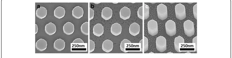
In this work, three different pore-patterned quartz moulds were employed, allowing the corresponding in-verse patterns to be defined. The replicated patterns consist of (a) 300-nm period hexagonal array of 180-nm (facet-to-facet dimension) hexagonal pillars/studs, (b) 300-nm period square array of 200 nm × 100-nm rect-angular pillars, and (c) 150-nm period hexagonal array of 50-nm diameter circular studs. By incorporating some de-gree of lateral etching in RIE after NIL to remove the re-sidual material in the recessed regions, NIL pillars/studs can be narrowed, thereby providing some tunability in the dimensions of the NIL features. The patterns are shown in Figure 2a,b,c.
The patterned area in each 300-nm period mould is 10 mm × 10 mm, while that for the 150-nm period mould is 5 mm × 5 mm, enabling equal-sized imprints to be replicated over a wafer surface. An instance of wafer-level nanoimprinting by SRNIL is shown in Figure 3. In this case, 32 nanoimprinted fields were generated over the surface of a 4″Si wafer. The street size between the fields can be varied to accommodate more or less fields. Fur-thermore, by virtue of the step-and-repeat mechanism, the NIL process can be extended for up to 8″wafers.
Metal-catalyzed electroless etching
The mechanism of MCEE is well discussed in literature and will not be described at length here [28]. Briefly, in a solution of HF and an oxidative agent, e.g., H2O2, of
[image:3.595.58.540.88.485.2]ap-propriate concentrations, regions of Si that are in con-tact with a noble metal, such as Au or Ag, are etched
much faster than those regions without metal coverage. This phenomenon arises because the noble metal acts as a catalyst facilitating the local injection of holes into Si, resulting in its oxidation and subsequent removal by HF. The reaction is redox in nature and the metal‘sinks’into Si, creating an etched path. Therefore, by pre-patterning a noble metal layer on Si prior to immersion in HF/H2O2,
patterned etched structures can be generated.
The steps leading up to MCEE for the stud-patterned wafers are described as follows and schematically shown
in Figure 4. After the removal of the residual material at the recessed regions by RIE, a thin layer of Au (approxi-mately 20-nm thick) acting as the catalyst was deposited by electron beam evaporation at a pressure of approxi-mately 10−6Torr. The wafer was then immersed in a so-lution of 4.6 M HF and 0.44 M H2O2 for the required
period of time, after which the reaction was halted by rapid removal of the wafer from the chemical solution and subsequent immersion in deionized water. Next, the Au layer was removed in aqua regia at 70°C, and the NIL mask was stripped in boiling piranha solution to re-veal the Si nanostructures.
[image:4.595.60.538.89.182.2]Results and discussion
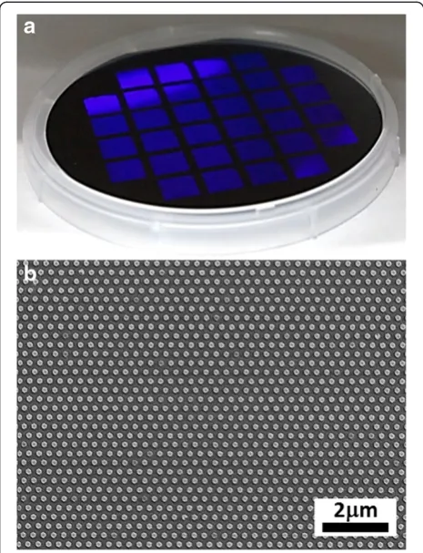
Figure 5a shows a 4″ Si wafer bearing 32 fields (each 10 mm × 10 mm) of hexagonal Si nanopillars in a hex-agonal arrangement generated by the aforementioned approach. The near-perfect ordering of the Si nanopillars can be deduced from the optically diffracted violet-blue light when the wafer was tilted at an angle against a diffused white light source. The near-perfect long-range ordering is also observed in the SEM image of Figure 5b. Figure 5c shows the closed-up SEM plan view of the hexagonal Si nanopillars. The period of the nanopillars is 300 nm (corre-sponding to an area density of 1.28 × 10⁷ pillars/mm2) as defined by the nanoimprinting mould, while the lateral facet-to-facet dimensions is approximately 160 nm, a re-duction from the approximately 180-nm pores in the NIL mould. The NIL mask which forms a cap over each nano-pillar is visible in the SEM images demonstrating the re-sistance of the material to attack by the HF/H2O2etching
solution. The inset of Figure 5b shows the SEM cross-section of the Si nanopillars, revealing the etched profiles, straight sidewalls, and NIL mask caps. The height of the etched hexagonal Si nanostructures is approximately proportional to the etching duration, indicating a near-constant etch rate (approximately 320 nm/min). By vary-ing the time of etchvary-ing, the height of the structures can be adjusted, thus tuning the aspect ratio.
Molar concentrations of HF and H2O2, abbreviated as
[HF] and [H2O2], respectively, other than that reported
in this work (4.6 M HF and 0.44 M H2O2), have been Figure 2SEM images of the nanoimprinted samples after RIE.Inset shows the respective cross-sections.(a)300-nm period hexagonal array of 180-nm (facet-to-facet) hexagonal pillars/studs,(b)300-nm period square array of 200-nm × 100-nm rectangular pillars, and(c)150-nm period hexagonal array of 50-nm diameter circular studs.
Figure 3Photograph of nanoimprinted 4″Si wafer (a) and SEM image showing long-range order of corresponding nanostructures (b).The wafer in(a), produced by SRNIL, was deliberately tilted at an angle to bring out the violet-blue tinge arising from the optical diffraction caused by the highly ordered nanoimprinted hexagonal studs of 300-nm periodicity.
Hoet al. Nanoscale Research Letters2013,8:506 Page 4 of 10
[image:4.595.57.290.362.666.2]employed in our experiments. However, it is found that 4.6 M HF and 0.44 M H2O2are optimal for rapidly
gener-ating high aspect ratio Si nanostructures with sidewalls of low porosity. Similar concentrations have also been used by other works reported in the literature [18,20,21,29,30]. The influence of [HF] and [H2O2] in fabricating the Si
nanostructures in MCEE has been discussed by Lianto [29] and Lianto et al. [31]. According to them, the porosity of the etched nanostructures is controlled by the
concentration of excess electronic holes in Si. Since the flux and consumption of the electronic holes depend on [H2O2] and [HF], respectively, these are crucial in
deter-mining the structure of the etched bodies and the etch rate. Higher [H2O2] is correlated with increased porosity
[image:5.595.57.540.89.409.2]because the flux of the electronic holes injected into Si is higher, and more excess holes can diffuse from the catalyst to cause porosity in other regions of the Si nanostructures. A similar phenomenon has been observed in our
Figure 4The generation of wafer scale, highly ordered Si nanostructures from a SRNIL nanoimprinted Si wafer via MCEE.
Figure 5Photograph and SEM images of wafer-scale Si nanostructures formed by the combined approach of SRNIL and MCEE. (a)
Photograph of a 4″Si wafer consisting of 32 arrays of hexagonally ordered hexagonal Si nanopillars.(b)SEM image showing the hexagonal long-range order of the Si nanopillars. Inset shows the cross-sectional SEM image of the Si nanopillars showing the relatively straight sidewalls and NIL mask cap.
[image:5.595.57.540.567.679.2]experiments and by Wang et al. [25] where higher [H2O2]
leads to increased sidewall roughness and structure poros-ity. However, even with increased [H2O2], etching occurs
much faster in the regions of Si covered by the Au catalyst such that a large degree of anisotropy is maintained, albeit at the expense of greater sidewall roughness and porosity, especially near the top of the Si nanostructures. Con-versely, a low [H2O2] is still insufficient to eliminate
por-osity in the Si nanostructures when [HF] is low, although it allows a slower, more controllable etch rate.
Increasing [HF] can significantly reduce the porosity of the sidewalls, while also increasing the etch rate [29]. Unfortunately, an excessively high [HF] leads to the in-creased evolution of H2bubbles which can interfere with
the spatial etch uniformity. As aforementioned, 4.6 M HF and 0.44 M H2O2are chosen as an optimal
combin-ation. However, lower concentrations, possibly in similar relative molar ratios, may also be employed to provide a slower etch rate but with minimal porosity for the gener-ation of lower aspect ratio Si nanostructures in MCEE. Hence, depending on the degree of nanoporosity and etch rate required, the concentration of the MCEE solu-tion can be suitably tuned.
Due to the lack of an etch stop layer in MCEE, con-trolled halting of the wet etching process requires rapid removal of the wafer from the etching solution and subse-quent immersion/rinsing in a bath of non-reacting dilution medium (deionized water in this case). This technique quenches the reaction, and good spatial control can be effected provided that the removal and immersion/rinsing steps can be executed in a much shorter time frame (ap-proximately 1 s, in our case) relative to the total etch time. Considering the etch rate of approximately 320 nm/min, etch depths of several hundreds of nanometers to more than a micron can be achieved with low relative spatial etch depth variation, since the absolute difference in spatial
etch depth represents only a small fraction of the height of the Si nanostructures. For shallower etch depths, a slower, more controlled etch rate would be recommended and can be achieved by lowering [HF] and [H2O2] but in suitable
molar concentration ratios. Large-scale reproducibility in large wafers may require suitable engineering control methods such as large baths of deionized water under con-stant agitation or rapidly flowing deionized water for quenching of reaction and rinsing.
Unlike other reported Si nanostructures produced by metal-assisted chemical etching which sports a highly roughened top surface due to chemical attack, with the degree of roughening increasing with etch duration [16-18,20,21,28], our technique produces Si nanostruc-tures with considerably smoother top surfaces. As shown in Figure 6, the top surface of the Si nanostructure re-mains well-defined and flat after MCEE and NIL mask removal. However, a slight narrowing of the hexagonal Si nanopillars (from approximately 180 nm to approxi-mately 160 nm) occurs with increased duration of etch-ing (from 30 to 180 s). This should be taken into consideration when fabricating Si nanostructures with low tolerance for dimensional deviations. While this lat-eral component of etching is much slower than the reac-tion occurring directly at the regions of Si covered by the Au catalyst, thus conferring a high degree of anisot-ropy to the MCEE process, it will nonetheless impose a limit to the maximum achievable aspect ratio. An aspect ratio as high as 20:1 has been obtained in our experi-ments, but the maximum value will likely be limited by dissolution of the Si nanowires [21]. Aspect ratios up to 220:1 have been achieved [19].
[image:6.595.54.541.532.654.2]While maintaining relatively low doping levels in the Si wafers (resistivity 10 to 20 Ω.cm) may play a con-tributory role in slowing the progress of porosity attack, the preservation of the smooth top surface is more likely
Figure 6Plan view SEM images of Si nanostructures after different etch durations with the NIL masks removed. (a)30-,(b)60-, and(c)180-s etch durations. The top surfaces of the nanostructures remain smooth after the process due to a good degree of protection offered by the NIL masking layer. This contrasts with the rougher sidewalls. Slight narrowing in the lateral dimensions of the Si nanostructures from approximately 180 nm to approximately 160 nm occurs when the etching duration is increased from 30 to 180 s. The fine lines or streaks observed in(b)and to a greater degree in(c)between the Si nanostructures are attributable to non-uniform gold coating of low-relief surfaces between higher structures prior to FESEM to reduce charging effects.
Hoet al. Nanoscale Research Letters2013,8:506 Page 6 of 10
linked to the use of the NIL mask. The latter is formed by the UV polymerization of a proprietary silicon-containing acrylate resist, the adhesion of which is strongly enhanced by the use of the planarization/primer layer. This is shown to be highly resistant to chemical attack by both acids and bases, with complete removal being effected by immersion in boiling piranha solution only. The NIL mask caps re-main after MCEE and are shown in Figure 5b,c. The obser-vations show that under our conditions of etching, the mask offers good protection to the Si surface against chem-ical attack by the HF/H2O2etching solution. The integrity
of the Si nanostructure is further shown in the high-resolution transmission electron microscopy (HR-TEM) images of Figure 7. A smooth morphology of the top sur-faces (Figure 7a,b) is observed in contrast to the rougher sidewalls (Figure 7c,d). The preservation of the top surface
can have potential device applications which are currently being explored.
[image:7.595.55.539.297.656.2]As shown in the magnified TEM images of Figure 7c,d, the bottom of the Si nanostructure has smoother sidewalls than the top because of shorter exposure to the etching solution, and this is consistent with reports in literature [16,28]. The selected area electron diffraction (SAED) pat-tern in Figure 7f is obtained from near the tip of a single nanorod. The sharp and clear SAED pattern is typical of a single-crystal face-centered cubic material like silicon, ob-served in the (011) beam direction. No stray spots or elongation of spots is observed, indicating that high crystal quality is maintained after the etching. Figure 7 shows that MCEE occurs largely along the <100 > direction away from the top surface of the Si(100) wafer. The observed anisotropy of MCEE in Si is consistent with the reports in
Figure 7HR-TEM images of metal-catalyzed electrolessly etched Si nanostructure (after a 60-s etch and removal of NIL mask). (a)Top left corner.(b)Top surface. The well-defined and flat top interface is a consequence of the resistance of the NIL mask against chemical attack.
(c)Left sidewall near the top surface. The etched sidewall shows a higher extent of surface roughness of about 3 nm due to attack by the HF/H2O solution.(d)Left sidewall towards base of nanostructure. Surface roughness is smaller due to shorter exposure to etching solution.
literature [16-18,20,21,28,32,33] and may be explained by the back-bond breaking theory [33,34]. Briefly, each atom on the (100) surface has only two back-bonds compared to three for that on the (110) and (111) surfaces, such that the former has a weaker back-bond strength. It is thus more easily removed during MCEE, and the etching oc-curs preferentially along the <100 > direction.
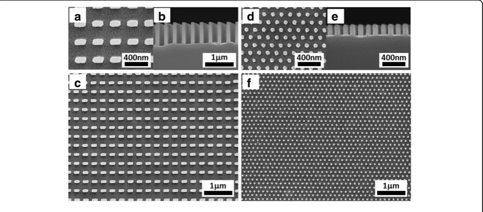
Other SRNIL patterns may similarly be transferred into the underlying Si substrate by MCEE. Figure 8 shows the Si nanostructures (190 ± 3 nm by 95 ± 2 nm rectangular cross-section and 46 ± 2-nm diameter circu-lar cross-section of pilcircu-lars) generated from the patterns in Figure 2b,c. The results demonstrate that the array configurations are not restricted to hexagonal arrange-ment alone and may be extended to square arrays too. In addition, the Si nanostructures may take on other cross-sectional shapes such as rectangular or circular profiles with feature dimensions down to sub-50 nm. Aspect ratios up to 20:1 or more have been achieved, but the compliant Si nanowires have a tendency to ad-here to each other due to surface tension forces exerted during processing, resulting in partial loss of ordered ar-rangement. In all, we believe that these patterns are suf-ficient to demonstrate the versatility in nanoscale Si pattern generation of our approach and may be employed for a myriad of applications including nano-scale field effect transistors [1-3], biological, and chem-ical sensing [8], electrodes in Li-ion batteries [10], and nanocapacitor arrays [11].
Our work provides evidence of the controllability of the ordering, shapes, and dimensions of MCEE nanostructures
by nanoimprinting, and general anisotropy in MCEE pro-files simply by appropriate substrate orientation selection, mask material selection and connectivity of the catalytic layer. Further, by taking advantage of the fact that NIL moulds can be written with arbitrary patterns not neces-sarily of simple regular or periodic designs, we posit that complex three-dimensional nanostructures [35,36] with applications in photonics and optoelectronics can similarly be generated on a manufacturing scale for widespread im-plementation. In fact, through SRNIL, the patterns can be varied across the wafer by employing differently patterned moulds. Other nanoscale patterning techniques, for in-stance, interference lithography, and short-range self-assembly methods like AAO patterning, block copolymer, and nanosphere lithography are limited to producing peri-odic arrays of rod or wire-like shapes. Parallel and large-area wafer-scale patterning, as well as repeated use of a single mould, is further afforded by SRNIL. These features make our approach of SRNIL with MCEE more practically useful than other approaches published previously. The realization of long-range ordering of high aspect ratio Si nanostructures at sub-50-nm resolution with the afore-mentioned pattern versatility and on a wafer scale has not yet been reported.
Conclusions
[image:8.595.60.539.475.685.2]In conclusion, we demonstrate the versatile pattern gen-eration of wafer-scale, highly uniform, well-ordered Si nanostructures with sub-50-nm resolution using a com-bination of step-and-repeat nanoimprint lithography and metal-catalyzed electroless etching. The long-range
Figure 8SEM images of Si nanostructures generated by SRNIL and MCEE. (a,b,c)Close-up, cross-section, and overview of a 300-nm period square array of 190 ± 3 nm by 95 ± 2 nm rectangular cross-section Si nanopillars.(d,e,f)Corresponding views of a 150-nm period hexagonal array of sub-50-nm (46 ± 2 nm) diameter cylindrical Si nanopillars.
Hoet al. Nanoscale Research Letters2013,8:506 Page 8 of 10
order and variability of nanoscale patterning offered in this approach cannot be achieved by self-organized methods of nanopatterning such as AAO templating, nanosphere lithography, and block copolymer self-assembly. Versatility in nanoimprint mould patterns al-lows this combinatory method to overcome the short-comings of interference lithography and yet produce nanoscale features, previously limited to research-scale E-beam lithography or deep UV photolithography, on a wafer scale. The Si nanostructures produced in our ap-proach show a high degree of fidelity as the user-defined SRNIL patterns, and retain non-porous top surfaces due to the substrate adherent, and chemically resistant SRNIL resin mask. This method is capable of producing high aspect ratio structures through a simple inexpen-sive wet etching setup. Minor lateral sidewall etching which arises from prolonged immersion in the etching solution reduces the dimensions of the Si nanostructures and should be taken into account in the design and fab-rication process. Bearing these in mind, our approach could be very useful for large-scale nanostructured de-vice production.
Abbreviations
AAO:Anodic aluminum oxide; EBL: Electron beam lithography; IL: Interference lithography; MACE: Metal-assisted chemical etching; MCEE: Metal-catalyzed electroless etching; NIL: Nanoimprint lithography; RIE: Reactive ion etching; SAED: Selected area electron diffraction; SEM: Scanning electron microscopy; SiNWs: Si nanowires; SRNIL: Step-and-repeat nanoimprint lithography; TEM: Transmission electron microscopy.
Competing interests
The authors declare that they have no competing interests.
Authors’contributions
JH conceived the idea and planned the experiments. JH and JD performed, analyzed, and optimized the step-and-repeat nanoimprint lithography process. JH performed the gold-assisted chemical etching and SEM. JH and QW carried out the TEM and analyzed the data. AT and SC participated in the design and coordination of the study. All the authors contributed to the preparation and revision of the manuscript, as well as, read and approved it.
Authors’information
JH and QW are Ph.D. candidates working on nanopatterning, fabrication, and growth of semiconductor nanostructures for photovoltaic and light-emission applications with the National University of Singapore (NUS). JD works on nanolithography and is with the Institute of Materials Research and Engineering (IMRE) of the Agency of Science, Technology and Research (A*STAR) in Singapore. AT is a Professor at the Department of Mechanical Engineering, NUS. SC is a Professor at the Department of Electrical and Computer Engineering, NUS.
Acknowledgements
This work was supported in part by the National University of Singapore (NUS), the Singapore-MIT Alliance (SMA), and the Agency of Science Technol-ogy and Research (A*STAR).
Author details
1NUS Graduate School for Integrative Sciences and Engineering, National
University of Singapore, Centre for Life Sciences, #05-01, 28 Medical Drive, Singapore 117456, Singapore.2Centre for Optoelectronics, Department of
Electrical and Computer Engineering, National University of Singapore, Block E3 02-07, Engineering Drive 3, Singapore 119260, Singapore.3Institute of
Materials Research and Engineering, Agency for Science Technology and Research (A*STAR), 3 Research Link, Singapore 117602, Singapore.
4Singapore-MIT Alliance, National University of Singapore, Block E4 04-10, 4
Engineering Drive 3, Singapore 117576, Singapore.5Department of Mechanical Engineering, National University of Singapore, Block EA 07-08, 9 Engineering Drive 1, Singapore 117576, Singapore.6Singapore-MIT Alliance for Research and Technology Center, 1 CREATE Way, #10-01 CREATE Tower, Singapore 138602, Singapore.
Received: 9 October 2013 Accepted: 23 November 2013 Published: 1 December 2013
References
1. Goldberger J, Hochbaum AI, Fan R, Yang P:Silicon vertically integrated nanowire field effect transistors.Nano Lett2006,6:973–977.
2. Heinzig A, Slesazeck S, Kreupl F, Mikolajick T, Weber WM:Reconfigurable silicon nanowire transistors.Nano Lett2011,12:119–124.
3. Cui Y, Zhong Z, Wang D, Wang WU, Lieber CM:High performance silicon nanowire field effect transistors.Nano Lett2003,3:149–152.
4. Garnett E, Yang P:Light trapping in silicon nanowire solar cells.Nano Lett
2010,10:1082–1087.
5. Pan C, Luo Z, Xu C, Luo J, Liang R, Zhu G, Wu W, Guo W, Yan X, Xu J, Wang ZL, Zhu J:Wafer-scale high-throughput ordered arrays of Si and coaxial Si/Si1–xGexwires: fabrication, characterization, and photovoltaic application.ACS Nano2011,5:6629–6636.
6. Shir D, Yoon J, Chanda D, Ryu J-H, Rogers JA:Performance of ultrathin silicon solar microcells with nanostructures of relief formed by soft imprint lithography for broad band absorption enhancement.Nano Lett
2010,10:3041–3046.
7. Zhang A, Kim H, Cheng J, Lo Y-H:Ultrahigh responsivity visible and infrared detection using silicon nanowire phototransistors.Nano Lett
2010,10:2117–2120.
8. Patolsky F, Zheng G, Lieber CM:Fabrication of silicon nanowire devices for ultrasensitive, label-free, real-time detection of biological and chemical species.Nat Protoc2006,1:1711–1724.
9. Boukai AI, Bunimovich Y, Tahir-Kheli J, Yu J-K, Goddard WA 3rd, Heath JR:
Silicon nanowires as efficient thermoelectric materials.Nature2008,
451:168–171.
10. Chan CK, Peng H, Liu G, McIlwrath K, Zhang XF, Huggins RA, Cui Y:
High-performance lithium battery anodes using silicon nanowires. Nat Nano2008,3:31–35.
11. Chang S-W, Oh J, Boles ST, Thompson CV:Fabrication of silicon nanopillar-based nanocapacitor arrays.Appl Phys Lett2010,
96:153108–153103.
12. Peng K, Fang H, Hu J, Wu Y, Zhu J, Yan Y, Lee S:Metal-particle-induced, highly localized site-specific etching of Si and formation of single-crystalline Si nanowires in aqueous fluoride solution.Chemistry–A Eur J2006,
12:7942–7947.
13. Peng KQ, Hu JJ, Yan YJ, Wu Y, Fang H, Xu Y, Lee ST, Zhu J:Fabrication of single-crystalline silicon nanowires by scratching a silicon surface with catalytic metal particles.Adv Funct Mater2006,16:387–394.
14. Seeger K, Palmer RE:Fabrication of silicon cones and pillars using rough metal films as plasma etching masks.Appl Phys Lett1999,74:1627–1629. 15. Mao P, Han J:Massively-parallel ultra-high-aspect-ratio nanochannels as
mesoporous membranes.Lab Chip2009,9:586–591.
16. Huang Z, Fang H, Zhu J:Fabrication of silicon nanowire arrays with controlled diameter, length, and density.Adv Mater2007,19:744–748. 17. Peng K, Zhang M, Lu A, Wong N-B, Zhang R, Lee S-T:Ordered silicon
nanowire arrays via nanosphere lithography and metal-induced etching. Appl Phys Lett2007,90:163123.
18. Huang J, Chiam SY, Tan HH, Wang S, Chim WK:Fabrication of silicon nanowires with precise diameter control using metal nanodot arrays as a hard mask blocking material in chemical etching.Chem Mater2010,22:4111–4116. 19. Chang S-W, Chuang VP, Boles ST, Ross CA, Thompson CV:Densely packed
arrays of ultra-high-aspect-ratio silicon nanowires fabricated using block-copolymer lithography and metal-assisted etching.Adv Funct Mater
2009,19:2495–2500.
20. Choi WK, Liew TH, Dawood MK, Smith HI, Thompson CV, Hong MH:
Synthesis of silicon nanowires and nanofin arrays using interference lithography and catalytic etching.Nano Lett2008,8:3799–3802. 21. de Johannes B, Nadine G, Jörg VW, Ulrich G, Volker S:Sub-100 nm silicon
22. Vieu C, Carcenac F, Pépin A, Chen Y, Mejias M, Lebib A, Manin-Ferlazzo L, Couraud L, Launois H:Electron beam lithography: resolution limits and applications.Appl Surf Sci2000,164:111–117.
23. Plachetka U, Bender M, Fuchs A, Vratzov B, Glinsner T, Lindner F, Kurz H:
Wafer scale patterning by soft UV-nanoimprint lithography. Microelectron Eng2004,73–74:167–171.
24. Ji R, Hornung M, Verschuuren M, van de Laar R, van Eekelen J, Plachetka U, Moeller M, Moormann C:UV enhanced substrate conformal imprint lithography (UV-SCIL) technique for photonic crystals patterning in LED manufacturing.Microelectron Eng2010,87:963–967.
25. Wang D, Ji R, Du S, Albrecht A, Schaaf P:Ordered arrays of nanoporous silicon nanopillars and silicon nanopillars with nanoporous shells. Nanoscale Res Lett2013,8:42.
26. Balasundaram K, Jyothi SS, Jae Cheol S, Bruno A, Debashis C, Mohammad M, Keng H, John AR, Placid F, Sanjiv S, Xiuling L:Porosity control in metal-assisted chemical etching of degenerately doped silicon nanowires.Nanotechnology2012,23:305304.
27. Kustandi TS, Loh WW, Gao H, Low HY:Wafer-scale near-perfect ordered porous alumina on substrates by step and flash imprint lithography. ACS Nano2010,4:2561–2568.
28. Huang Z, Geyer N, Werner P, de Boor J, Gosele U:Metal-assisted chemical etching of silicon: a review.Adv Mater2011,23:285–308.
29. Lianto P:Mechanism and catalyst stability of metal-assisted chemical etching of silicon.Singapore-MIT Alliance: National University of Singapore; 2013. 30. Dawood MK, Liew TH, Lianto P, Hong MH, Tripathy S, Thong JTL, Choi WK:
Interference lithographically defined and catalytically etched, large-area silicon nanocones from nanowires.Nanotechnology2010,21:205305. 31. Lianto P, Yu S, Wu J, Thompson CV, Choi WK:Vertical etching with isolated
catalysts in metal-assisted chemical etching of silicon.Nanoscale2012,
4:7532–7539.
32. Peng K, Wu Y, Fang H, Zhong X, Xu Y, Zhu J:Uniform, axial-orientation alignment of one-dimensional single-crystal silicon nanostructure arrays. Angew Chem Int Ed2005,44:2737–2742.
33. Peng K, Lu A, Zhang R, Lee S-T:Motility of metal nanoparticles in silicon and induced anisotropic silicon etching.Adv Funct Mater2008,18:3026–3035. 34. Morinaga H, Suyama M, Ohmi T:Mechanism of metallic particle growth
and metal‐induced pitting on Si wafer surface in wet chemical processing.J Electrochem Soc1994,141:2834–2841.
35. Hildreth OJ, Lin W, Wong CP:Effect of catalyst shape and etchant composition on etching direction in metal-assisted chemical etching of silicon to fabricate 3D nanostructures.ACS Nano2009,3:4033–4042. 36. Hildreth OJ, Fedorov AG, Wong CP:3D spirals with controlled chirality
fabricated using metal-assisted chemical etching of silicon.ACS Nano
2012,6:10004–10012.
doi:10.1186/1556-276X-8-506
Cite this article as:Hoet al.:Versatile pattern generation of periodic, high aspect ratio Si nanostructure arrays with sub-50-nm resolution on a wafer scale.Nanoscale Research Letters20138:506.
Submit your manuscript to a
journal and benefi t from:
7 Convenient online submission 7 Rigorous peer review
7 Immediate publication on acceptance 7 Open access: articles freely available online 7 High visibility within the fi eld
7 Retaining the copyright to your article
Submit your next manuscript at 7 springeropen.com
Hoet al. Nanoscale Research Letters2013,8:506 Page 10 of 10