CYCLIC VOLTAMMETRY MEASUREMENT FOR N-TYPE Cu2O THIN
FILM USING COPPER ACETATE-BASED SOLUTION
Asyikin Sasha binti Mohd Hanif, Fariza binti Mohamad, Razmi Zafiruddin bin Zakaria
Department of Electronic Engineering, Faculty of Electrical and Electronic Engineering, Universiti Tun Hussein Onn Malaysia, Parit Raja, 86400, Batu Pahat, Johor, Malaysia.
Email: [email protected]
ABSTRACT
Cyclic voltammetry (CV) measurement are used to determine the ideal potential range to deposit n-type cuprous oxide by electrodeposition method on fluorine-doped tin oxide (FTO) glass substrate using copper (II) acetate-based solution. Conventional methods of fabrication were time and cost consuming due to no ideal parameter setup. With cyclic voltammetry measurement, redox reaction could be obtained. Hence, the parameters for fabrication process were optimized. Electrodeposition method was used to deposit the cuprous oxide thin film onto the FTO glass substrate. The selected pH values for this study were pH 5.5 and 6.5 with deposition temperature of 50 and 60°C. The deposition time was fixed to 60 minutes. N-Cu2O thin films were fabricated and then characterized using Field
Emission Scanning Electron Microscopy, X-Ray Diffractometer, Ultraviolet-Visible Spectroscopy and surface profiler. From the results of the analyses, the band gap obtained was 1.8 eV. The structural, morphological and optical properties showed that cuprous oxide with (111) preferred orientation were successfully fabricated.
Keywords: Cuprous oxide Cyclic voltammetry Electrodeposition N-type semiconductor
INTRODUCTION
Solar cell has emerged as one of the top research for harvesting one of the important sustainable energy sources, solar energy. Harvesting solar energy does not affect the environment as the energy is produced by the sun. Sunlight from the sun can be used directly to generate electricity using photovoltaic technology [1-3]. The typical material of a solar cell is silicon. However, the high cost of using the silicon solar cells to capture light energy have forced the development in creating new photovoltaic devices that utilize cheap and non-toxic materials prepared by energy-efficient process [4].
One of the substituting material for solar cell application is a metal oxide semiconductors, cuprous oxide (Cu2O). The synthesized Cu2O is typically a p-type
semiconductor with a direct band gap of around 2.0 – 2.2 eV which makes it a potential candidate for light energy absorbing layer in solar cell plates. Besides, Cu2O is
attractive due to its high absorption coefficient, comes in abundance, non-toxicity and low cost fabrication [5-7].
There are many methods have been applied to produce Cu2O thin film which include sol-gel approach
[8], thermal oxidation [7], chemical vapour deposition [9], sputtering [10] and electrochemical method [11, 12]. In this study, electrochemical process is chosen because the deposition process is simple, inexpensive, producing controllable film thickness, producing large scale deposition and can be done at low temperature [13, 14]. Moreover, it has the ability to control the surface morphologies, phase compositions and other elements by adjusting the deposition parameters [15]. By using this method, the type of Cu2O semiconductor can be
determined by varying the pH of Cu2O electrolyte
solution. An alkaline condition which is higher than pH 9 will produce a p-type Cu2O semiconductor while an acidic
condition with pH lower than 7.0 will produce an n-type Cu2O semiconductor [16].
Conventional electrodeposition process of thin film is time consuming because the experiment takes longer time to find an ideal potential value for Cu2O
deposition and thus contributed to high cost of process [17, 18]. Thus, an additional process prior to electrodeposition process is suggested which is cyclic voltammetry. Cyclic voltammetry is a simple and direct method for measuring the formal potential of a half reaction when both oxidized and reduced forms are stable during the time required to obtain the voltammograms (current-potential curves) [19]. In this study, cyclic voltammetry was used to plot the ideal region of potential range for n-type Cu2O thin film deposited at different
solution pH and different solution temperature.
EXPERIMENTAL
A. FTO Substrate and Cu2O solution preparation
Cu2O thin films were deposited on FTO substrates via
electrodeposition method. Prior to the deposition process, substrates were cut in 2.5 cm x 1.0 cm dimensions, cleaned with acetone in ultrasonicator for 5 min and rinsed with distilled water. An opening area of 1 cm x 1 cm for Cu2O deposition was created and the remaining area was
covered with kapton tape. The substrates were further cleaned using polarization process with a galvanostat setting of 10 mA/cm2 for 60 s.
The solution used for n-Cu2O deposition on FTO substrate
was copper acetate-based solution. 200 mL aqueous solution was made up from mixtures of 0.4 M of copper (II) acetate monohydrate, 3 M of lactic acid and potassium hydroxide (KOH). pH of Cu2O solution was fixed to pH
B. Cyclic voltammogram (CV) measurement and analysis
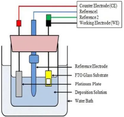
For this section, the experimental setup was set as in Figure 1. Before executing CV, the setup was tested using open circuit test for rest potential determination as the values are different according to solution pH and temperature. Then, the rest potential was used as the starting and end potential for the CV process. Generally, the potential range applied for this process was between -1.5 V to +1.0 V vs reference electrode (Ag/AgCl). The parameters values were set to 50 and 60 °C for solution temperature and pH 5.5 and 6.5 for solution pH.
Figure 1: Experimental setup for cyclic voltammetry and electrodeposition process of Cu2O solution.
C. Cu2O electrodeposition process
In order to fabricate Cu2O thin film layer,
electrodeposition method (Solartron Analytical, 1280C Electrochemical Test System) was used. The experimental setup for this process was the same as in Section B. However, only one potential value was used for deposition which was determined from CV process. The varied parameters remained the same which were the solution pH and temperature.
D. Characterization and analysis
Several characterization tests were done on the electrodeposited Cu2O thin film. The structural
characterization was done using X-Ray Diffractometer (XRD) (Bruker, Model D8 Advance), Field Emission Scanning Electron Microscopy (FESEM) (JEOL, Model JSM-7600F) for morphological characterization and Ultra Violet-Visible (UV-Vis) Spectroscopy (Shimadzu, Model UV 1800) for optical analysis.
RESULT AND DISCUSSION
A. Cyclic voltammetry measurement
As previously mentioned, CV measurement was used to find the ideal region to deposit the n-type Cu2O thin film.
It was done by applying sweeping potential from one potential value to a minimum potential then to a maximum potential and back to the first potential. For this measurement, the applied potential was from rest potential
to -1.5 V and sweep to +1.0 V and back to rest potential vs Ag/AgCl. The rest potential (+0.1 V) was obtained from open circuit test which was applied before running the CV measurement.
[image:2.595.309.547.185.280.2] [image:2.595.62.272.203.401.2]Two main parameters were varied in this experiment which were the solution temperature and pH. For each temperature, two samples of different pH value were used. As shown in Table 1, the temperature values used were 50 °C and 60 °C while the pH values used were pH 5.5 and pH 6.5, respectively.
Table 1: Deposition parameters Sample Solution
Temperature (°C)
Solution pH
1 50 5.5
2 50 6.5
3 60 5.5
4 60 6.5
Figure 2 and 3 show the cyclic voltammetry plot for all samples. Different pH value of the Cu2O electrolyte with
different temperature resulted in different range of oxidation and reduction process. By assuming the regions marked in Figure 2 and Figure 3 were the ideal range to deposit n-type Cu2O thin film, a potential value was
selected for each sample. The main reduction process in this study is shown by:
From Figure 2 that shows deposition temperature of 50 °C, the current densities drastically dropped indicating a quite narrow potential region for n-Cu2O deposition which was
approximately between -0.1 V to -0.02 V vs Ag/AgCl. In Figure 3, the potential region for n-Cu2O deposition at 60
[image:2.595.314.555.537.696.2]°C was larger which was approximately between -0.2 V to 0 V vs Ag/AgCl. The selected potential for deposition of n-Cu2O was stated in Table 2.
Figure 3: Cyclic voltammetry plot for temperature 60 °C. Table 2: Deposition parameter with selected potential.
B. Structural characterization
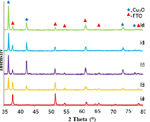
By using XRD, the structural state of Cu2O
electrodeposited on FTO substrate in different pH at different solution temperature were characterized. Figure 4 shows the stacked XRD pattern of all samples. In all samples, the XRD peaks were consistent with the standard peaks in JCPDS no. 050667 which determined the success formation of Cu2O [20]. The peaks detected were at 36.4°,
42.3°, 52.5° and 73.5° corresponding to Cu2O plane (111),
(200), (211) and (311), respectively as shown in Table 3. The focused peak for fabrication of Cu2O was the
reflection at (111) formation which in this study, Sample 4 showed the highest peak. This indicates the structural improvement of Cu2O crystallinity.
Figure 4: XRD spectrum for (a) FTO substrate, (b) Sample 1, (c) Sample 2, (d) Sample 3 and (e) Sample 4.
Table 3: Corresponding plane for Cu2O reflection peaks.
C. Morphological characterization
Figures 5, 6, 7 and 8 shows the morphological evolution of Cu2O thin films that were deposited under different
solution pH at different solution temperature. FESEM images revealed the strong effect of deposition parameters towards composition and microstructure of Cu2O thin
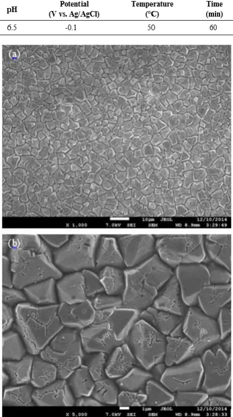
films. Figure 5 shows the surface morphology for Sample 1 which was done using the parameters showed in Table 4. From figure, it can be seen that there were some triangular shapes which believed to represent Cu2O shape [21]. The
[image:3.595.50.287.295.373.2]5K magnification image shows an individual triangular shape while the 1K magnification shows the thin films were forming several group of small islands with nanoflower shape.
[image:3.595.293.542.348.757.2]Table 4: Deposition parameter for Sample 1.
[image:3.595.56.305.559.762.2]Sample 2 was fabricated using parameter shown in Table 5. Figure 6 shows the FESEM image of Sample 2 which at 5K magnification, there were some triangular shapes that represent Cu2O. The 1K magnification image shows
evenly grown Cu2O on the substrate. There were no spaces
or gap between the grains. This indicated that at solution temperature 50 °C, Cu2O solution with pH 6.5 was more
[image:4.595.53.285.178.593.2]homogenously deposited on FTO substrate compared to Cu2O solution with pH 5.5.
Table 5: Deposition parameter for Sample 2.
Figure 6: FESEM image of Sample 2 with (a) 1K and (b) 5K magnification.
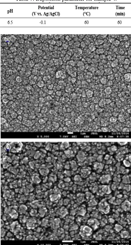
Figure 7 shows Sample 3 fabricated using parameters shown in Table 6. As can be seen, there were also some triangular shape on the sample but with smaller grain compared to Sample 1 and 2. The structures were also not uniform on FTO substrate. While in Figure 8, Sample 4 was fabricated using parameters as shown in Table 7. The grain sizes were significantly smaller but they were covering all the substrate with no gaps can be seen on the images. The small triangular shapes corresponding to Cu2O were observed clearly on FTO substrate. The
morphological characteristics of n-Cu2O thin film were
consistent with the structural properties.
Some correlations can be concluded by doing morphological characterization. The temperature of Cu2O
solution affected the grain size of Cu2O thin film. At one
pH value, the sample with higher solution temperature exhibited smaller grain compared to lower temperature. The pH of Cu2O solution affected the shape and
distribution of Cu2O on the FTO substrate. At pH 5.5 with
different temperatures, Cu2O deposited in groups that
[image:4.595.310.545.230.647.2]formed nanoflower-like shape. The grains were not homogenously distributed. While at pH 6.5 with different temperature, the triangular shapes are more evenly distributed on FTO substrate.
Table 6: Deposition parameter for Sample 3.
Table 7: Deposition parameter for Sample 4.
Figure 8: FESEM images of Sample 4 with (a) 1K and (b) 5K magnification.
D. Optical analysis
The absorbance of the samples was obtained from the result of UV-Vis analysis. The absorbance spectrums were used to calculate the band gap of the sample. The band gap was pointed out from the Tauc Plot which was the coefficient (αhv)1/2 versus the photon energy (eV). Figure
[image:5.595.315.545.53.212.2]9 shows the absorbance spectrum of the samples while Figure 10 shows the Tauc plot which was obtained from manipulating the data from the absorbance. The band gap for Sample 4 was 1.8 eV which is around the bandgap energy of Cu2O.
[image:5.595.52.283.58.487.2]Figure 9: Plot of absorbance versus wavelength for Sample 4.
Figure 10: Plot of (αhv)1/2 versus the photon energy (eV)
for Sample 4.
CONCLUSION
N-type Cu2O thin film were successfully fabricated onto
FTO glass substrate by using electrodeposition method. Cyclic voltammetry measurements were used in order to understand the redox process and to obtain the ideal parameter range for deposition of Cu2O thin film. From
CV measurements, n-Cu2O with different temperature and
pH were prepared. All samples were homogenously grown on FTO glass substrate with typical triangular shape of Cu2O except Sample 1 that exhibited nanoflower-shape of
Cu2O. The structural properties of Cu2O were analysed
and all samples possessed (111) preferred orientation. Among these samples, Sample 4 showed optimum structural properties. Cu2O was homogenously fabricated
on the FTO substrate. This sample also absorbed light at wavelength 600 nm with the band gap energy of 1.8 eV. In conclusion, n- Cu2O thin film was successfully fabricated
[image:5.595.315.554.256.457.2]ACKNOWLEDGEMENTS
The authors would like to acknowledge Microelectronic and Nanotechnology Shamsuddin Research Center (MINT-SRC), Universiti Tun Hussein Onn Malaysia for providing laboratory apparatus and characterization equipment for this study. This work was supported by Fundamental Research Grant Scheme (FRGS) Vote No. 1223.
REFERENCES
[1] Goetzberger, A., C. Hebling, and H.-W. Schock,
Photovoltaic materials, history, status and outlook.
Materials Science and Engineering: R: Reports, 2003.
40(1): p. 1-46.
[2] Goetzberger, A., J. Luther, and G. Willeke, Solar cells: past, present, future. Solar Energy Materials and Solar Cells, 2002. 74(1–4): p. 1-11.
[3] Green, M.A., Photovoltaics: technology overview.
Energy Policy, 2000. 28(14): p. 989-998.
[4] Wöhrle, D. and D. Meissner, Organic Solar Cells.
Advanced Materials, 1991. 3(3): p. 129-138.
[5] Fernando, C.A.N. and S.K. Wetthasinghe,
Investigation of photoelectrochemical characteristics of n-type Cu2O films. Solar Energy Materials and Solar Cells, 2000. 63(3): p. 299-308.
[6] Han, K. and M. Tao, Electrochemically deposited p–n homojunction cuprous oxide solar cells. Solar Energy Materials and Solar Cells, 2009. 93(1): p. 153-157. [7] Musa, A.O., T. Akomolafe, and M.J. Carter,
Production of cuprous oxide, a solar cell material, by thermal oxidation and a study of its physical and electrical properties. Solar Energy Materials and Solar Cells, 1998. 51(3–4): p. 305-316.
[8] Akhavan, O., H. Tohidi, and A.Z. Moshfegh, Synthesis and electrochromic study of sol–gel cuprous oxide nanoparticles accumulated on silica thin film. Thin Solid Films, 2009. 517(24): p. 6700-6706.
[9] Jeong, S. and E.S. Aydil, Heteroepitaxial growth of Cu2O thin film on ZnO by metal organic chemical vapor deposition. Journal of Crystal Growth, 2009. 311(17): p. 4188-4192.
[10] Akimoto, K., et al., Thin film deposition of Cu2O and application for solar cells. Solar Energy, 2006. 80(6): p. 715-722.
[11] Xue, J., et al., Preparation and formation mechanism of smooth and uniform Cu2O thin films by electrodeposition method. Surface and Coatings Technology, 2013. 216(0): p. 166-171.
[12] McShane, C.M., Junction Studies on Electrochemically Fabricated P-N Cu2O Homojunction Solar Cells for Efficiency Enhancement. Phys Chem Chem Phys, 2012. 14(17): p. 6112-6118.
[13] Bugarinovic, S., et al., Cuprous Oxide as an Active Material for Solar Cells, in Solar Cells: New Aspects and Solutions, L.A. Kosyachenko, Editor 2011, Intech: Croatia. p. 167-186.
[14] Katayama, J., et al., Performance of Cu2O/ZnO Solar Cell Prepared by Two-Step Electrodeposition. Journal of Applied Electrochemistry, 2004. 34(7): p. 687.
[15] Chen, L.-C., Review of preparation and optoelectronic characteristics of Cu2O-based solar cells
with nanostructure. Materials Science in Semiconductor Processing, 2013. 16(5): p. 1172-1185.
[16] Siripala, W., et al., Study of annealing effects of cuprous oxide grown by electrodeposition technique.
Solar Energy Materials and Solar Cells, 1996. 44(3): p. 251-260.
[17] Shahrestani, S.M., Electrodeposition of Cuprous Oxide for Thin Film Solar Cell Applications, 2013, University in Montreal: Quebec.
[18] Wang, L. and M. Tao, Fabrication and Characterization of p-n Homojunctions in Cuprous Oxide by Electrochemical Deposition. Electrochemical and Solid-state Letters, 2007. 10(9): p. 248-250.
[19] Evans, D.H., et al., Cyclic Voltammetry. Journal of Chemical Education, 1983. 60(4): p. 290.
[20] Laidoudi, S., et al., Growth and characterization of electrodeposited Cu 2 O thin films. Semiconductor Science and Technology, 2013. 28(11): p. 115005. [21] Papadimitropoulos, G., et al., Deposition and