Design and Simulation of Output Queuing with the
Middle stage Buffered (OQMB) Clos Packet Switching
Network
S. Rajeshwari
M.E (Applied Electronics)
University college of Engineering Nagercoil Kanyakumari, Tamilnadu, India
R. Bharathi,
Assistant professor University college of Engineering NagercoilKanyakumari, Tamilnadu, India
ABSTRACT
Clos network, a family of multistage networks, are attractive alternative for constructing scalable packet switches because of its distributed and modular design. The clos packet switching networks are the next step in scaling current crossbar switches to large number of ports. This paper presents the design and simulation of buffer less- buffered-buffered - Clos Packet switching network architecture. This paper proposes a novel the output queuing with the middle stage buffered (OQMB) Clos Packet switching architecture that does not need any schedulers. This architecture employs an ID matching with OQMB packet switching and desynchronize static round robin (DSRR) scheme to achieve Maximum throughput under any admissible traffic. Our queuing analysis demonstrates that only small size buffers are needed in the central stage. The only trade off for the proposed (OQMB) architecture is to employ small extra resequencing buffers. Input modules with desynchronize static round robin (DSRR) scheme connection scheme guarantees no cell contention in input stages. As a result, the OQMB architecture can achieve very high performance, and high throughput under any admissible traffic.
General words
Output Queuing with the Middle stage Buffered (OQMB), Desynchronize Static Round Robin (DSRR), Input and Output Queuing (IOQ)
Keywords
Input and Output Queuing with the Middle stage Buffered (IOQMB), Fully Buffered (FB),Very Large Scale Integration (VLSI).
1. INTRODUCTION
Clos network is a kind of multistage on chip permutation network. The Clos network architecture [1] was first proposed by C. Clos in the 1950s, for use in telecommunications networks. Clos networks are required, when the physical circuit switching needs exceed the capacity of the largest feasible single crossbar switch. We proposed to design and simulation of a Clos packet switching network to support collision free and guaranteed throughput. The combinatorial properties of this multi-stage interconnected network help to construct strict non-blocking circuit switches with fewer cross-points. Clos networks have three stages: the ingress stage, middle stage, and the egress stage. Each stage is made
up of a number of crossbar switches; often just called crossbars.This network has a rearrangeable property [11] that can realize all possible permutations between its input and outputs. The choice of the three stage Clos network with a modest number of middle stage switches is to minimize implementation cost, whereas it still enables a rearrangeable property for the network. The proposed clos network employs an ID matching with OQMB packet switching and desynchronize static round robin (DSRR) scheme. The ID matching scheme offers a contention free routing from unauthorized users. It compares the user ID with the switch port ID, depending upon ID matching it will allows the segmented packets to further stages. The output queuing with the central stage buffered (OQMB) clos packet switching network contains buffer less input stage with the buffered central stage and buffered output stage. A desynchronized static round-robin (DSRR) connection pattern is set in buffer less input stage switching modules and guarantees zero cell contention. This paper is organized as follows; section 2, explains related work of clos packet switching network design. Section 3, explains a brief introduction of clos packet switching network design is presented. Section 4 gives the simulation Results. In section 5, gives the conclusion.
2. RELATED WORK
Reviewing on chip permutation networks (supporting either full or partial permutation) with regard to their implementation shows that most of the networks employ a packet switching mechanism to deal with the conflict of permutated data [3]–[6]. Their implementations either use first input first output (FIFO) queues for the conflicting data [3] [5] [6] or time slot allocation in the overall system with the cost of more routing stages [5] or a complex routing with a deflection technique that avoids buffering of the conflicting data [4]. The choices of network design factors, i.e., topology, switching technique and the routing algorithm, have different impacts on the on chip implementation. Regarding the routing algorithm, the deflection routing [4] is not energy efficient due to the extra hops needed for deflected data transfer, compared to a minimal routing [2] [3] [5]. Moreover, the deflection makes packet latency less predictable; hence, it is hard to guarantee the latency and the in order delivery of data. Clos-network packet switch can be classified based on their buffer (memory) allocation schemes. For example, the simplest Clos-network fabric has no buffers at any stage.
buffered (IOQMB) architecture has buffered input and output stages and a buffer less central stage. Although there are other possible buffer allocation schemes a fully buffered architecture, most existing researches on Clos-network packet switch are on these two architectures. Their focus is to develop good scheduling algorithms for the architectures. In fact, the way of allocating the buffers is an important design consideration and it influences the switching performance. Buffer less architecture is favoured for hardware simplicity. However pure space switching in all three stages increases the cell contention probability. The throughput of buffer less with random dispatching may be as low as 39.7%. Input and output queuing with the buffer less central stage (IOQ) architecture tries to enhance the performance of buffer less by adding buffers to input and output stages. The buffers relieves the cell
[image:2.595.59.537.254.644.2]contentions in these two stages, but IOQ tends to keep a buffer less central stage in fear the of out-of-sequence problem. This leaves some unsolved contentions. The throughput of IOQ with random dispatching is increased but not satisfactory. The worst case throughput is 63% and is still not a satisfied result. Obviously, Fully Buffered (FB) architecture does not suffer any throughput degradation since all possible contentions are absorbed by buffers, but it is expensive to be implemented. It is worth asking whether there exists less complex architecture which performs as well as Fully Buffered (FB). Observing that the main effect of buffers is to resolve contentions, buffers can be removed if there is no contention at all. The proposed clos network employs an ID matching with OQMB packet switching and desynchronize static round robin (DSRR) scheme.
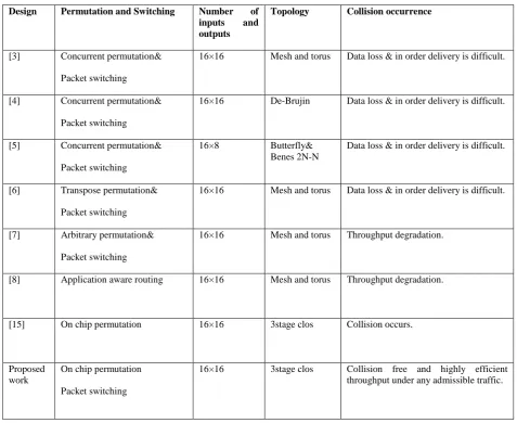
Table 1 Comparison with other related on-chip permutation networks
Design Permutation and Switching Number of
inputs and
outputs
Topology Collision occurrence
[3] Concurrent permutation&
Packet switching
16×16 Mesh and torus Data loss & in order delivery is difficult.
[4] Concurrent permutation&
Packet switching
16×16 De-Brujin Data loss & in order delivery is difficult.
[5] Concurrent permutation&
Packet switching
16×8 Butterfly& Benes 2N-N
Data loss & in order delivery is difficult.
[6] Transpose permutation&
Packet switching
16×16 Mesh and torus Data loss & in order delivery is difficult.
[7] Arbitrary permutation&
Packet switching
16×16 Mesh and torus Throughput degradation.
[8] Application aware routing 16×16 Mesh and torus Throughput degradation.
[15] On chip permutation 16×16 3stage clos Collision occurs.
Proposed work
On chip permutation
Packet switching
16×16 3stage clos Collision free and highly efficient throughput under any admissible traffic.
3.
CLOS
PACKET
SWITCHING
NETWORK DESIGN
Clos network, a family of multistage networks, is applied to build scalable commercial multiprocessors with thousands of nodes in macro systems [7] [11]. AS typical three stage Clos network is defined as C (n, m, p), where n represents the number of inputs in each of p stage switches and m is the number of second stage switches. The proposed clos network
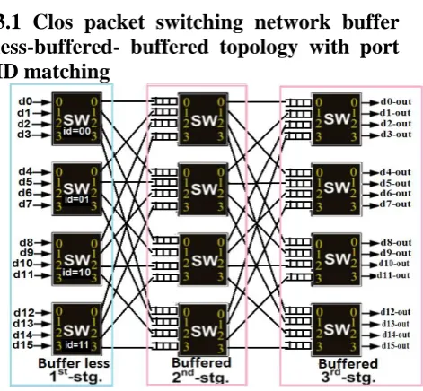
3.1 Clos packet switching network buffer
less-buffered- buffered topology with port
ID matching
Fig 3.1: Clos packet switching network
This paper proposed to use C (4, 4, 4) as a topology for the designed network (Fig.3.1). This network has a rearrangeable property [11] that can realize all possible permutations between its input and outputs.Fig1 says that there are sixteen input ports are available in our clos network. These ports are connected to the corresponding switches depending upon the ID of the switches .The first switch is having the ID as 00, second switch is having the ID as 01, Third switch is having the ID as 10 and fourth switch is having the ID as 11. The proposed clos network employs an ID matching with OQMB packet switching and desynchronize static round robin (DSRR) scheme. A desynchronized static round-robin (DSRR) connection pattern is set in buffer less input stage switching modules and guarantees zero cell contention. OQMB architecture is proved to be of 100% throughput under any admissible traffic. It needs no scheduler and is practical to be implemented. In response to the out-of-sequence problem, queuing analysis is conducted for output queues of the central stage.
[image:3.595.319.544.332.402.2]3.2 Proposed Block Diagram
Fig 3.2: Block Diagram
Fig3.2. Shows that the ID matching section matches switch ID with the port ID and connect it to the output port. If it is not matching means it would not allow that so it makes the collision free one from un authorized users. Due to the clos network topology all possible combinations are available between inputs to output. The output queuing with the middle stage buffered OQMB packet switching architecture consists of a buffer less input stage, buffered middle and output stages. In packet switching, messages are broken into certain blocks called packets, and packets are transmitted independently using the store and forward scheme. The packets are passed to the first stage. Each packet contains the packet number, Source address and destination address. The buffer less input
stage forwards the packet to the second depending on the destination address using DSRR connection pattern. The buffered central stage Stores the packet and forwards it by FIFO Principle to the destination by using destination address. . The buffered output stage Stores the packet and forwards it by FIFO Principle to the destination port. After receiving packet third stage sends the Ack signal to the source If it sends the Negative Ack means again the source will resend the packet.
3.3 Desynchronized static round-robin
(DSRR) connection pattern
DSRR is run distributed and independently by each Input stage. Any input sequentially connects to all outputs in a round-robin manner; at each time slot, inputs map injectively to outputs. This can be achieved by setting a fully desynchronized initial Connection pattern input stage with DSRR connection scheme guarantees no cell contention in input stages when the fabric is non-blocking (i.e., m ≥ n). This is because at each time slot, there is at most one cell arrives at the Input stage, and it is immediately transferred to an output stage according to the connection pattern. Cells arriving at the input stages are dispatched to different Central stages within a time slot.
Fig 3.3: Desynchronized static round-robin (DSRR)
3.4 Packet transmission
[image:3.595.318.532.537.620.2]The buffer less input stage forwards the packet to the second depending on the destination address. The buffered central stage Stores the packet and forwards it by FIFO Principle to the destination by using destination address. . The buffered output stage Stores the packet and forwards it by FIFO Principle to the destination port. After receiving packet third stage sends the Ack (01) signal to the source. If it sends the Negative Ack (11) means again the source will resend the packet.
Fig 3.4: Packet transmission
[image:3.595.56.279.548.624.2]4. SIMULATION RESULTS
[image:4.595.317.556.70.194.2]4.1 First stage switch with ID matching
Fig 4.1: First stage switch with ID matching
The Fig 4.1 shows that the clock signals as high and switch1 id as 00. This is matches with switch id so allows it. Then the first port of SW_1/d0 sends the packet to third output port SW_1/d3 out by sending 00111111.In this first 4 bit represents output address and next four bit represents packet data.
4.2 Router stage switch output
Fig 4.2.1: Packet transmission
Fig 4.2.1 shows thatfirst port of SW_1/d0 sends the packet data 1111 to the third output port SW_1/d3 out by sending the destination address and data 00111111.In this first 4 bit represents destination address and next four bit represents packet data. This is the expanded view of each bit.
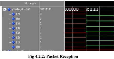
Fig 4.2.2: Packet Reception
Fig 4.2.2 shows the SW_1/d3 out receives the packet 1111 Successfully
[image:4.595.56.299.107.305.2]4.3 First stage data flow diagram
Fig 4.3: First stage data flow
Fig 4.3 shows the dataflow of First stage. Here the clock signal as high and first port of SW_1/d0 sends the packet to third output port SW_1/d3 out by sending 00111111.In this first 4 bit represents output address and next four bit represents packet data.
[image:4.595.315.563.245.404.2]4.4 Router stage data flow diagram
Fig 4.4: Router stage data flow
Fig 4.4 shows the dataflow of router stage. Here the clock signal as high and first port of SW_1/d0 sends the packet to third output port SW_1/d3 out by sending 00111111.In this first 4 bit represents output address and next four bit represents packet data. The final stage SW_1/d3 out receives the packet 1111 Successfully.
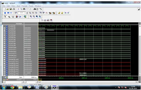
[image:4.595.53.296.408.544.2] [image:4.595.316.563.497.672.2]4.5 Router stage wave output
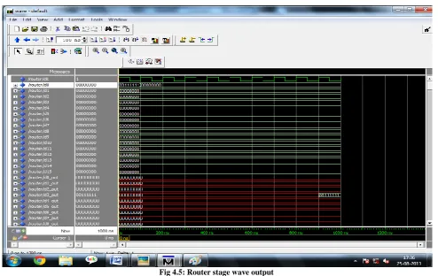
[image:5.595.55.544.481.697.2]Fig 4.5: Router stage wave output
Fig 4.5 shows therouter stage wave output here the first port of SW_1/d0 sends the packet data 1111 to the third output port SW_1/d3 out by sending the destination address and data
00111111.In this first 4 bit represents destination address and next four bit represents packet data. The final stage SW_1/d3 out receives the packet 1111 Successfully
4.6 Router stage list output
Fig 4.6: Router stage list output
4.7 Router stage packet flow diagram
Fig 4.7: Router stage packet flow diagram
Fig 4.5 shows therouter stage packet flow diagram .Here the packet flows through two paths simultaneously .Switch 1 first port forwards the packet through the second stage first port to destination. At the same time the packet flows through second
stage fifth port to destination .Then the re ordering of the packet is done in the d3_out and successfully receives the packet
4.8 Router stage Acknowledgement diagram
Fig 4.8: Router stage Acknowledgement diagram
Fig 4.8 shows the Router stage Acknowledgement diagram. Here Ack is received as 01 to Sw_1/d-0 from third output port SW_1/d3 out. Finally Switch1 d_0 input port successfully makes the contention free path with the third output port by
receiving 00000100.In this first 4 bit represents the source address next two bit(01) is Ack bit and next two bit is header. If source receives negative Ack(11) then re transmission will
be performed
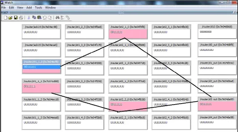
4.9 Router stage simultaneous packet transmission
Fig 4.9: Router stage packet transmission
Fig 4.8 shows the Router stage simultaneous packet transmission here router /d0 sends the packet 1111 to d8_out, router/d5 sends the packet 1110 to d0_out and router /d11 sends the packet 0000 to d7_out.With the help of buffering all these packets are successfully received with contention free and improves efficiency.
5. CONCLUSION
In this Paper, We have presented the output queuing with the middle stage buffered (OQMB) Clos Packet switching network architecture. This OQMB Clos Packet switching architecture is designed using buffer less input stage – buffered central stage – buffered output stage - Clos Packet switching network. This network architecture is designed using VHDL .After designing this architecture using VHDL codings are simulated using ModelSim 6.3.This architecture employs an ID matching with OQMB packet switching and desynchronize static round robin (DSRR) scheme to achieve
6. REFERENCES
[1] S. Borkar, “Thousand core chips—A technology perspective,” in Proc. ACM/IEEE Design Autom. Conf. (DAC), 2007, pp. 746–749.
[2] P.-H. Pham, P. Mau, and C. Kim, “A 64-PE folded-torus intra-chip communication fabric for guaranteed throughput in network-on-chip based applications,” in Proc. IEEE Custom Integr. Circuits Conf. (CICC), 2009, pp. 645–648.
[3] C.Neeb, M. J.Thul, and N. Wehn, “Network-on- chip-centric approach to interleaving in high throughput
channel decoders,” in Proc. IEEE Int. Symp. Circuits Syst. (ISCAS), 2005, pp. 1766–1769.
[4] H. Moussa, A. Baghdadi, and M. Jezequel, “Binary de Bruijn on-chip network for a flexible multiprocessor LDPC decoder,” in Proc. ACM/ IEEE Design Autom. Conf. (DAC), 2008, pp. 429–434.
[5] H. Moussa, O. Muller, A. Baghdadi, and M. Jezequel, “Butterfly and Benes-based on-chip communication networks for multiprocessor turbo decoding,” in Proc. Design, Autom. Test in Euro. (DATE), 2007
[6] S. R. Vangal, J. Howard, G. Ruhl, S. Dighe, H. Wilson, J. Tschanz, D. Finan, A. Singh, T. Jacob, S. Jain, V. Erraguntla, C. Roberts, Y. Hoskote, N. Borkar, and S. Borkar, “An 80-tile sub-100-w TeraFLOPS processor in 65-nm CMOS,” IEEE J. Solid-State Circuits, Jan. 2008.
[7] W. J. Dally and B. Towles, Principles and Practices of Interconnection Networks: San Francisco, CA: Morgan Kaufmann, 2004.
[8] N. Michael, M. Nikolov, A. Tang, G. E. Suh, and C. Batten, “Analysis of application-aware on-chip routing under traffic uncertainty,” in Proc. IEEE/ACM Int. Symp. Netw. Chip (NoCS), 2011.
[9] P.-H. Pham, J. Park, P. Mau, and C. Kim, “Design and implementation of backtracking wave-pipeline switch to support guaranteed throughput in network-on-chip,” IEEE Trans. Very Large Scale Integr. (VLSI)Syst.,
[10]D. Ludovici, F. Gilabert, S. Medardoni, C. Gomez, M. E. Gomez, P.Lopez, G. N. Gaydadjiev, and D. Bertozzi, “Assessing fat-tree topologies for regular network-on-chip design under nanoscale technology constraints,” in Proc. Design, Autom.
[11]Y. Yang and J.Wang, “A fault-tolerant rearrangeable permutation network,” IEEE Trans. Comput., vol. 53, no. 4, Apr. 2004.
[12]P. T. Gaughan and S. Yalamanchili, “A family of fault-tolerant routing protocols for direct multiprocessor networks,” IEEE Trans. ParallelDistrib. Syst., vol. 6, no. 5, May 1995.
[13] V. E. Beneš, “Mathematical Theory of Connecting Networks and TelephoneTraffic”. New York: Academic Press, 1965.
[14]F. Safaei a,c, A. Khonsari a,b, M. Fathy c, M. Ould-Khaoua “Pipelined circuit switching: Analysis for the torus with non-uniform traffic”
[15]Phi-Hung Pham, Junyoung Song, Jongsun Park, and Chulwoo KimDesign and Implementation of an On-Chip Permutation Network for Multiprocessor System On-Chip
[16]C. Clos, A Study of Non-Blocking Switching Networks, Bell Sys. Tech. Jour., pp. 406-424, March 1953.
[17]F. M. Chiussi, J. G. Kneuer, and V. P. Kumar, Low-Cost Scalable Switching Solutions for Broadband Networking: the ATLANTA Architecture and Chipset, IEEE Commun. Mag., pp. 44-53, vol. 35, issue 12, Dec 1997.
[18]K. Pun and M. Hamdi, Distro: A Distributed Static Round-Robin Scheduling Algorithm for Bufferless Clos-Network Switches, GLOBECOM ’02, pp. 2298-2302, Vol. 3, Nov. 2002.
[19]E. Oki, Z. Jing, R. Rojas-Cessa, and J. chao, concurrent Round-Robin- Based Dispatching Schemes for Clos-Network Switches, IEEE Trans. On Clos-Networking, pp. 830-844, Vol. 10, issue 6, Dec 2002.
[20]Xin Li, Zhen Zhou and Mounir Hamdi “Space-Memory-Memory Architecture for Clos-Network Packet Switches”
7. AUTHOR’S PROFILE
S.Rajeshwari was born in tamilnadu, India in 1989. She received her B.E degree from PET Engineering College, Vallioor, and Tamilnadu in 2010 and she is doing her M.E degree in University College of Engineering, Nagercoil.
R. Bharathi was born in tamilnadu; India in 1977.She received her B.E degree from NoorulIslam college of Engineering, Kanyakumari, Tamilnadu in 1998. And she received her M.E degree from Arulmigu Kalasalingam College of engineering, Tamilnadu in 2006 .She is working as an Assistant Professor in Department of ECE, University College of Engineering, Nagercoil.