2019 International Conference on Information Technology, Electrical and Electronic Engineering (ITEEE 2019) ISBN: 978-1-60595-606-0
Influence of Quantum Dot Layer on the Properties of Quantum Dot Light
Emitting Diodes
Hang MA and Deng-hua LI
*School of Automation, Beijing Information Science & Technology University, Beijing 100192, China
*Corresponding author
Keywords: Quantum dot light emitting diodes, Electroluminescent, Quantum dot concentration, Quantum dot type.
Abstract. In order to research the influence of quantum dot luminescent layer on the properties of quantum dot light emitting diodes (QLEDs), samples of QLEDs with the structure of ITO/PEDOT:
PSS/Poly-TPD/CdSe/CdS/ZnS/Alq3/Al were fabricated through spin coating and vacuum
evaporation technologies. Experiment results show that with the quantum dot concentration being fixed to 8 mg/ml, the devices have good electroluminescent properties and excitons recombination luminescent region is mainly located in the quantum dot layer. Based on the determination of concentration of quantum dot, samples of QLEDs with the structure of ITO/PEDOT: PSS/Poly-TPD/GA_CdSe/ZnS/ZnO/Al and ITO/PEDOT: PSS/Poly-TPD/CdSe/CdS/ZnS/ZnO/Al were fabricated. Experiment results show that when the quantum dot type is CdSe/CdS/ZnS, the
devices emit red spectral radiation with high brightness up to 5225 cd/m2 and have no defect state
luminescence in contrast to the device using GA_CdSe/ZnS as the quantum dot luminescent layer. The research results have directive significance on the fabrication of QLEDs.
Introduction
Quantum dot light emitting diodes (QLEDs) are superior to organic light emitting diodes (OLEDs) because of their unique potential properties, including narrow luminescence spectrum, wide range of visual angle, high color purity and tunable emission wavelength, therefore they have broad application prospects and have the greatest potential to become the core part of the next generation display devices [1-4]. Since the first luminous phenomenon of QLED was reported by Colvin [5], how to realize the equilibrium of carrier injection and improve the luminescence performance of QLED has attracted increasing attention in the field of QLEDs. Sun et al. [6] fabricated QLEDs with different colors through selecting different particle sizes of quantum dots (QDs). In their researches, the carrier injection balance in the QDs layer was controlled by changing the thickness of the electron
transport layer (ETL) Alq3. However, the devices had a high turn-on voltage and poor stability as Alq3
was an organic material which was susceptible to water and oxygen and had lower electron mobility. Zaiats et al. [7] fabricated red emitting QLEDs by using CIZS as QDs layer, PVK and TPD with similar energy levels as hole transport layer (HTL). In their experiment, they found that the voltage and efficiency of the QLEDs were not only related to energy levels, bus also affected by conductance and charge transformation. In order to improve the carrier injection balance, Dai et al. [8] embedded the insulating material PMMA between the QDs layer and ETL, and prepared the red emitting QLEDs. They exhibited high external quantum efficiencies (EQE) of up to 20.5%. Gu et al.[9] demonstrated
Si based QLEDs can work much more efficiently after using HAT-CN and MoO3 between ITO and
PEDOT:PSS as a interlayer. This structure increased the surface work function of ITO and promoted the injection of holes, therefore the EQE and the stability of QLEDs were improved. Wang et al. [10]
fabricated the inverted green QLEDs by using mixed MoO3 and HAT-CN as hole injection layer
(HIL). As compared with the reference device with a single MoO3 or HAT-CN as the HIL, this device
maximum EQE reached 12.7% and 5.99% for red and blue QLEDs, which exhibited the best performance among all the all-solution processed inverted QLEDs. Ma et al. [12] imbedded an
electron blocking layer TPD into the QDs/Alq3 interface. Through controlling the thickness of the
TPD, they found that a thinner thickness and lower LUMO should be chosen when selecting the electron blocking layer. At the same year, Ma et al. [13] studied the mechanism of carrier injection. In their researches, models based on the Fowler-Nordheim (FN) tunneling injection and space-charge limited current (SCLC) conduction were simulated to analyze the injection situation of carriers, and the optimal thickness of HTL was confirmed. Also they fabricated the QLEDs, the experiment results were basically agree with the simulation results.
In this paper, samples of QLEDs with the structure of ITO/PEDOT:
PSS/Poly-TPD/CdSe/CdS/Zns/Alq3 were fabricated by using different concentrations of QDs at first,
and the influence of concentrations of QDs on current density, voltage and spectrum were analyzed. Based on the determation of concentration of QDs, samples of QLEDs with the structure of ITO/PEDOT: PSS/Poly-TPD/GA-CdSe/Zns/ZnO and samples of QLEDs with the structure of ITO/PEDOT: PSS/Poly-TPD/CdSe/CdS/ZnS/ZnO were fabricated. And the electroluminescent spectra of the two devices were analyzed under different voltages. The results provided gudance for the effective fabrication of QLEDs.
Experimental Methods
Fabrication of the QLEDs
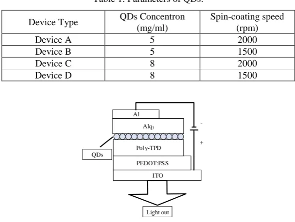
[image:2.595.145.449.446.675.2]In order to study the influence of QDs concentration, the QLEDs were fabricated at first, with the structure consisting of layers of ITO (185 nm)/PEDOT:PSS (35 nm) /poly-TPD (45 nm) /CdSe/CdS/ZnS/Alq3 (30 nm) /Al (100 nm). The parameters of the CdSe/CdS/ZnS (QDs) are shown in Table 1 and the structure is shown in Figure 1.
Table 1. Parameters of QDs.
Device Type QDs Concentron (mg/ml)
Spin-coating speed (rpm)
Device A 5 2000
Device B 5 1500
Device C 8 2000
Device D 8 1500
-ITO PEDOT:PSS Pol y-TPD
Alq3 Al
QDs
+
Light out
Figure 1. Device structure of QLED.
The QLEDs were fabricated as follows. Firstly, the pre-patterned and polished ITO substrates were cleaned in various solvents, then the surfaces of the substrates were blown dry with nitrogen. Finally, the ITO substrates were treated with UV/ozone for 20 min to increase the surface work function and reduce the injection barrier. PEDOT:PSS solutions were spin-coated onto the ITO substrates at 4000
rpm for 40 s and baked at 140C for 10 min, then the substrates were placed in a glove box filled with
nitrogen. Poly-TPD (in chlorobenzene, 8 mg/ml) were deposited by spin coating at 1500 rpm for 40 s
and CdSe/CdS/ZnS (in toluene, 5 mg/ml) were spin-coated on the different Poly-TPD surfaces at 2000 rpm and 1500 rpm respectively for 40 s and baked at 80 C for 20 min. Alq3 and Al were
deposited using a thermal evaporation system under a high vacuum of 2×10⁻⁶ torr.
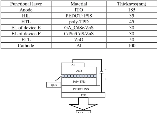
In order to study the influence of QDs types, the QLEDs with the structure consisting of layers of ITO (185 nm)/PEDOT:PSS (35 nm) /poly-TPD (45 nm) /GA_CdSe/ZnS (30 nm)/ZnO (50 nm) /Al (100 nm) were fabricated. And the QLEDs with the structure consisting of layers of ITO (185 nm)/PEDOT:PSS (35 nm) /poly-TPD (45 nm) / CdSe/CdS/ZnS (30 nm)/ZnO (50 nm) /Al (100 nm) were also fabricated. The parameters of the QLEDs are shown in Table 2 and the structure is shown in Figure 2. The fabrication methods of the structure of Figure 2 was as same as the methods of the structure of Figure 1, except that the ETL was ZnO. And ZnO (in alcohol, 25mg/ml) were spin-coated
[image:3.595.136.460.252.484.2]on the QDs surface at 2000 rpm for 40 s and baked at 145 C for 20 min.
Table 2. Parameters of QLEDs.
Functional layer Material Thickness(nm)
Anode ITO 185
HIL PEDOT: PSS 35
HTL poly-TPD 45
EL of device E GA_CdSe/ZnS 30
EL of device F CdSe/CdS/ZnS 30
ETL ZnO 50
Cathode Al 100
-ITO PEDOT:PSS Pol y-TPD
ZnO Al
QDs
+
Light out
Figure 2. Device structure of QLED.
Measurement of the QLEDs Characteristics
The current density-voltage characteristics were measured by Keithley 2410. The voltages and currents were obtained through a computer-controlled Keithley 2410, and then the data were stored in the computer. The current density -voltage characteristic curves of QLEDs were calculated according to the light-emitting area of the QLEDs. The luminance and luminescent spectrum were measured by Topcon’s SR-3AR spectroradiometer.
Experimental Results and Analysis
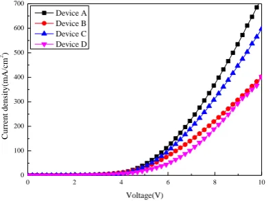
Influence of QDs Concentration on QLEDs Performance
speed of spin coater. And the growth rate of the current density of device C is also much higher than that of the device D. According to the above analyses, it can be conclude that the influence of speed of spin coater on the current density is greater than that of the QDs concentration when the QDs concentration is not much different.
0 2 4 6 8 10
0 100 200 300 400 500 600 700
C
u
rr
en
t
d
en
si
ty
(mA
/cm
2)
Voltage(V) Device A
[image:4.595.197.393.145.292.2]Device B Device C Device D
Figure 3. Current density-voltage characteristics at different concentrations and speeds.
Figure 4 and 5 show the electroluminescence (EL) spectra of device B and D at different voltages respectively. As can been seen in Figure 4, nearly 50% of the detected electroluminescence comes
from the Alq3, and the devices not only exhibit the red light of QDs with peak emission wavelength of
625 nm, but also exhibit the green light of Alq3 with the peak emission wavelength of 520 nm when
the QDs concentration is 5 mg/ml. As the voltage increases, both the red and green light EL intensity increase, and meanwhile, the spectra appear red shift. These effects indicate that the exciton recombination region lies between QDs layer and ETL. The carrier injection in the QDs layer is extremely unbalanced, especially the generation of green light, which greatly reduces the color purity of the QLEDs and seriously affects the performance of the QLEDs.
400 500 600 700 800
0.0 0.2 0.4 0.6 0.8 1.0
EL in
ten
si
ty
(a.u
.)
Wavelength(nm) 5 V
[image:4.595.194.399.472.626.2]6 V 7 V 8 V
Figure 4. EL spectra of device B.
probability to form excitons. But the QDs concentration should not be too high, otherwise the thickness of the QDs layer formed by spin coating will be too thick. Thick film will lead to lower transmission rate of the carrier which increases the turn-on voltage and affects the device efficiency. From the experiment results and analyses above, it can be concluded that the QLEDs have good luminous properties which are easily regulated when the QDs concentration is 8 mg/ml.
400 500 600 700 800
0.0 0.2 0.4 0.6 0.8 1.0
EL in
ten
si
ty
(a.u
.)
Wavelength(nm) 5 V
[image:5.595.200.395.158.309.2]6 V 7 V 8 V
Figure 5. EL spectra of device D.
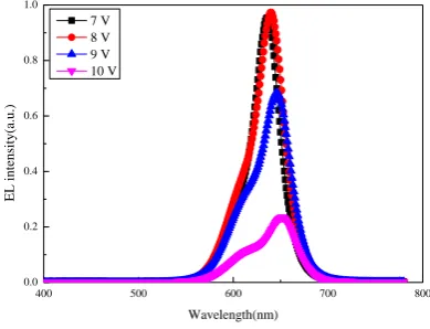
[image:5.595.197.392.581.730.2]Influence of QDs Type on QLEDs Performance
Figure 6 shows the EL spectra of device E at different voltages. As can be seen, with the increase of voltage, the asymmetry of red light spectra become more and more obvious, and the shoulder peak appears near 620 nm. This effect can be explained by QDs defect luminescence, and the radiation recombination comes from the defect levels of QDs or the impurities of band gaps. Since QDs are nanomaterials with large specific surface area, most of the defect states come from the QDs surface. On the one hand, these surface defects can easily capture photo-induced carriers and excitons formed by hole and electron recombination, which will increase the probability of non-radiative recombination, reduce the luminescence efficiency and affect the performance of QLEDs. On the other hand, QDs are easily oxidized by oxygen in the air, which will lead to QDs fluorescence quenching. However, in certain conditions, the excitons trapped by surface defects also radiate luminescence. For example, Djurisic et al. [14,15] found that the ZnO powders could exhibit green defect state luminescence in their researches. In our experiment, the luminescence of QDs defect states affects the uniqueness of the spectra and leads to the decrease of the color purity of the device, thus adversely affects the performances of the QLEDs.
400 500 600 700 800
0.0 0.2 0.4 0.6 0.8 1.0
EL in
ten
si
ty
(a.u
.)
Wavelength(nm) 7 V
8 V 9 V 10 V
Figure 6. EL spectra of device E.
voltage is 9 V, the luminance of the device reaches a maximum luminance value of 5225 cd/m2, the peak wavelength is at about 628 nm, and there in no defect state luminescence. The emission radiation recombination of excitons mainly comes from band edge emission. It can be seen from the above that the performance of QLEDs using the CdSe/CdS/ZnS as the emitting layer is superior to that of QLEDs using GA_CdSe/ZnS as the emitting layer.
400 500 600 700 800
0.0 0.2 0.4 0.6 0.8 1.0
Voltage=9 V Luminance=52259 cd/m2
EL in
ten
si
ty
(a.u
.)
Wavelength(nm) 4 V
[image:6.595.192.396.159.312.2]7 V 9 V 10 V
Figure 7. EL spectra of device F.
Summary
In summary, samples of QLEDs with different QDs concentrations were fabricated. Through comparing the current density-voltage characteristics and electroluminescent spectra of different QLEDs, we obtain that the QLEDs have better performances when the QDs concentration is 8 mg/ml. On the basis of the QDs concentration confirmed to be 8 mg/ml, samples of QLEDs with different QDs type were fabricated. The experimental results show that when the QDs type is CdSe/CdS/ZnS,
the device emits bright QDs red spectral radiation with the luminance up to 5225 cd/m2. The emission
radiation recombination of excitons mainly comes from band edge emission and the devices have no defect state luminescence. When the QDs type is GA_CdSe/ZnS, the defect state luminescence starts to appear and the red light spectra of QDs are asymmetrical. These phenomena indicate that the performances of CdSe/CdS/ZnS type QLEDs are superior to that of the GA_CdSe/ZnS type QLEDs. The research results have guiding significance for the fabrication of QLEDs.
Acknowledgement
This research was financially supported by National Program on Key Basic Research Project of China (973 Program) (No. 2015CB654605) and Foundation of Beijing information science & technology University (No. 5221810914).
References
[1] S. Coe, W.K. Woo, M. Bawendi, V. Bulovic, Electroluminescence from single monolayers of
nanocrystals in molecular organic devices, Nature. 420 (2002) 800-803.
[2] M.C. Schlamp, X. Peng, A.P. Alivisatos, Improved efficiencies in light emitting diodes made
with CdSe (CdS) core/shell type nanocrystals and a semiconducting polymer, J. Appl. Phys. 82 (1997) 5837-5842.
[3] P.O. Anikeeva, J.E. Halpert, M.G. Bawendi, V. Bulovic, Quantum dot light-emitting devices with
[4] G.J. Supran, Y. Shirasaki, K.W. Song, J.M. Caruge, P.T. Kazlas, S. Coe-Sullivan, T.L. Andrew, M.G. Bawendi, V. Bulovic, QLEDs for displays and solid-state lighting, Mrs. Bull. 38 (2013) 703-711.
[5] V.L. Colvin, M.C. Schlamp, A.P. Alivisatos, Light-emitting diodes made from cadmium selenide
nanocrystals and a semiconducting polymer, Nature. 370 (1994) 354-357.
[6] Q. Sun, Y.A. Wang, L.S. Li, D. Wang, T. Zhu, J. Xu, C. Yang, Y. Li, Bright, multicoloured
light-emitting diodes based on quantum dots, Nat. Photonics. 1 (2007) 717-722.
[7] G. Zaiats, S. Ikeda, S. Kinge, P.V. Kamat, Quantum dot light-emitting devices: beyond alignment
of energy levels, ACS Appl. Mater. Interfaces. 9 (2017) 30741-30745.
[8] X. Dai, Z. Zhang, Y. Jin, Y. Niu, H. Cao, X. Liang, L. Chen, J. Wang, X. Peng, Solution-processed,
high-performance light-emitting diodes based on quantum dots, Nature. 515 (2014) 96-99.
[9] W. Gu, X. Liu, X. Pi, X. Dai, S. Zhao, L. Yao, D. Li, Y. Jin, M. Xu, D. Yang, G. Qin, Silicon
quantum-dot light-emitting diodes with interlayer-enhanced hole transport, IEEE Photonics. J. 9 (2017) 1-10.
[10]L.S. Wang, Y. Lv, J. Lin, J. Zhao, Y. Wang, X. Liu, High-efficiency inverted quantum dot
light-emitting diodes with enhanced hole injection, Nanoscale. 9 (2017) 6748-6754.
[11]Y. Liu, C. Jiang, C. Song, J. Wang, L. Mu, Z. HE, Z, Zhong, Y. Cun, C, Mai, J. Wang, J. Peng, Y.
Cao, Highly Efficient All-Solution Processed Inverted Quantum Dots Based Light Emitting Diodes, ACS nano. 12 (2018) 1564-1570.
[12]H. Ma, D. Li, W. Chen, J. Ye, Influence of thickness of electron transport layer and block layer on
the properties of quantum dot light emitting diodes, Chin. J. Lumin. 38 (2017) 85-90.
[13]H. Ma, D. Li, W. Chen, J. Ye, Quantum dot light emitting diodes with ZnO electron transport
layer, Chin. J. Lumin. 38 (2017) 507-513.
[14]A.B. Djurišić, Y.H. Leung, W.C.H. Choy, K.W. Cheah, W.K. Chan, Visible photoluminescence in
ZnO tetrapod and multipod structures, Appl. Phys. Lett. 84 (2004) 2635-2637.